

Page 1
DAC 3550A
Stereo Audio DAC
6251-109-4E
Edition July 23, 1999
6251-467-1DS
MICRONASMICRONASMICRONASMICRONAS
MICRONAS
Page 2

DAC 3550A
Contents
Page Section Title
3 1. Introduction
3 1.1. Main Features
5 2. Functional Description
52.1.I
6 2.2. Interpolation Filter
6 2.3. Variable Sample and Hold
6 2.4. 3rd-order Noise Shaper and Multibit DAC
6 2.5. Analog Low-pass
6 2.6. Input Select and Mixing Matrix
6 2.7. Postfilter Op Amps, Deemphasis Op Amps, and Line-Out
7 2.8. Analog Volume
7 2.9. Headphone Amplifier
8 2.10. Clock System
8 2.10.1. Standard Mode
8 2.10.2. MPEG Mode
92.11.I
9 2.12. Registers
9 2.13. Chip Select
9 2.14. Reduced Feature Mode
2
SInterface
2
C Bus Interface
10 3. Specifications
10 3.1. Outline Dimensions
10 3.2. Pin Connections and Short Descriptions
12 3.3. Pin Descriptions
12 3.3.1. Power Supply Pins
12 3.3.2. Analog Audio Pins
12 3.3.3. Oscillator and Clock Pins
13 3.3.4. Other Pins
13 3.4. Pin Configuration
14 3.5. Pin Circuits
15 3.6. Control Registers
17 3.7. Electrical Characteristics
17 3.7.1. Absolute Maximum Ratings
18 3.7.2. Recommended Operating Conditions
20 3.7.3. Characteristics
25 4. Applications
25 4.1. Line Output Details
25 4.2. Recommended Low-Pass Filters for Analog Outputs
26 4.3. Recommendations for Filters and Deemphasis
26 4.4. Recommendations for MegaBass Filter without Deemphasis plus 1st-order low-pass
27 4.5. Power-up/down Sequence
27 4.5.1. Power-up Sequence
27 4.5.2. Power-down Sequence
28 4.6. Typical Applications
32 5. Data Sheet History
2 Micronas
Page 3
DAC 3550A
Stereo Audio DAC
1. Introduction
The DAC 3550A is a single-chip, high-precision, dual
digital-to-analog converter designed for audio applications. The employed conversion technique is based on
oversampling with noise-shaping.
With Micronas’ unique multibit sigma-delta technique,
less sensitivity to clock jitter, high linearity, and a superior S/N ratio has been achieved. The DAC 3550A is
controlled via I
Digital audio input data is received by a versatile I
2
C bus.
2
interface. The analog back-end consists of internal
analog filters and op amps for cost-effective additional
external sound processing. The DAC 3550A provides
line-out, headphone/speaker amplifiers, and volume
control. Moreover, mixing additional analog audio
sources to the D/A-converted signal is supported.
The DAC 3550A is designed for all kinds of applications in the audio and multimedia field, such as:
MPEG players, CD players, DVD players, CD-ROM
players, etc. The DAC 3550A ideally complements the
MPEG 1/2 layer 2/3 audio decoder MAS 3507D.
No crystal required for standard applications with
sample rates from 32 to 48 kHz. Crystal required
only for automatic sample rate detection below 32 kHz,
MPEG mode (refer to Section 2.10), and use of clock
output CLKOUT.
1.1. Main Features
– no master main input clock required
– integrated stereo headphone amplifier and mono
speaker amplifier
–SNR of 103dBA
2
C bus, I2S bus
–I
– internal clock oscillator
– full-feature mode by I
2
C control (three selectable
subaddresses)
S
– reduced feature mode for non-I
2
C applications
– continuous sample rates from 8 kHz to 50 kHz
– analog deemphasis for 44.1 kHz
– analog volume and balance: +18…
−75 dB and mute
– oversampling and multibit noise-shaping technique
– THD better than 0.01 %
– two additional analog stereo inputs (AUX) with
source selection and mixing
– supply range: 2.7 V…5.5 V
– low-power mode
– additional line-out
– on-chip op amps for cost-effective external analog
sound processing
WSI
CLI
DRI
I2S
Interpolation
Filter
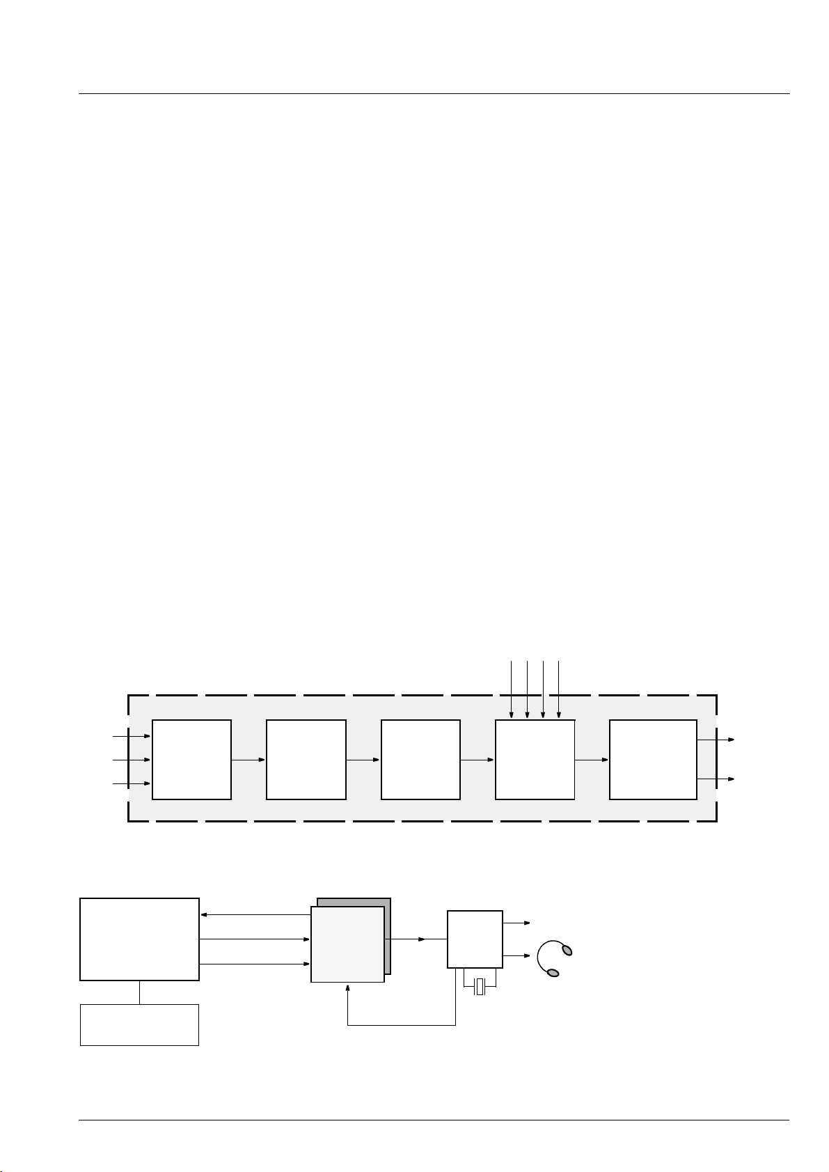
Fig. 1–1: Block diagram of the DAC 3550A
demand signal
Host
(PC, Controller)
ROM, CD-ROM,
RAM, Flash Mem. ..
MPEG clock
MPEG bit stream
3507D
MAS
CLKOUT
DAC
I2S
Analog Inputs
DAC
3550A
14.725 MHz
Input
Select
and
Mixing
line out
Volu me
and
Headphone
Amplifier
OUTL
OUTR
Fig. 1–2: Typical application: MPEG Layer 3 Player
Micronas 3
Page 4
DAC 3550A
CLI DAI WSI
23 24 25
I2S
Digital Supply
18
Vdd
17
Vss
CLKOUT
XTO
XTI
AUX2L
AUX1L
Sample Rate
Detection
14
13
Osc.
12
29
31
PLL
Interpolation Filter
Variable S & H
3rd-order Noise Shaper
&
Multibit DAC
Analog Low-pass Filter
Input Select
Switch Matrix
Analog
Supply
I2C
Control
9
10
3
2
44
1
16
15
27
26
21
19
20
32
30
AVDD0
AVDD1
AVS S0
AVS S1
VREF
AGNDC
SDA
SCL
TESTEN
PORQ
DEECTRL
MCS1
MCS2
AUX1R
AUX2R
FOPL
FINL
34
38
37
39
DEEML
FOUTL
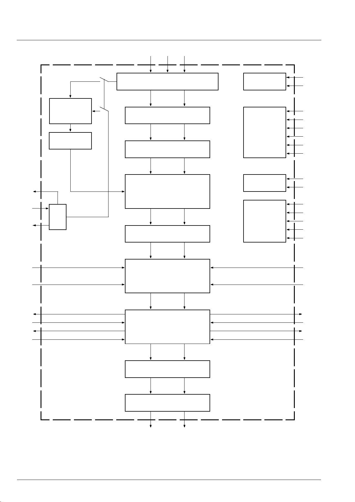
Fig. 1–3: Block diagram of the DAC 3550A
Postfilter Op Amps
Deemphasis Op Amps
Line-Out
Analog Volume
Headphone Amplifier
57
OUTROUTL
35
42
41
43
DEEMR
FOPR
FOUTR
FINR
4 Micronas
Page 5
DAC 3550A
2. Functional Description
2
S Interface
2.1. I
2
The I
S interface is the digital audio interface between
the DAC 3550A and external digital audio sources
such as CD/DAT players, MPEG decoders etc. It covers most of the I
2
S-compatible formats.
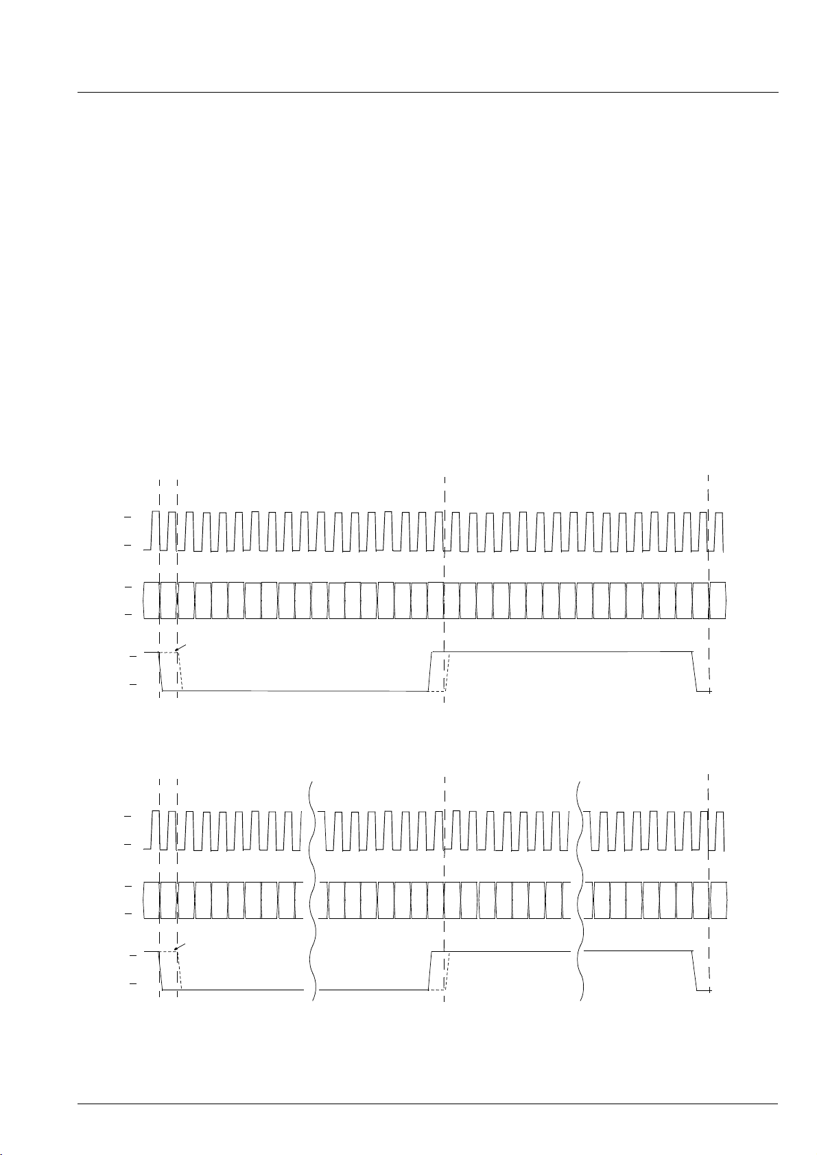
All modes have two common features:
2
1. The MSB is left justified to an I
S frame identifica-
tion (WSI) transition.
2. Data is valid on the rising edge of the bit clock CLI.
16-bit mode
In this case, the bit clock is 32
× fs
. Maximum word
audio
length is 16 bit.
32-bit mode
In this case, the bit clock is 64
× fs
. Maximum word
audio
length is 32 bit.
Automatic Detection
2
C control is required to switch between 16- and
No I
32-bit mode. It is recommended to switch the
DAC 3550A into mute position during changing
between 16- and 32-bit mode.
For high-quality audio, it is recommended to use the
32-bit mode of the I
2
S interface to make use of the full
dynamic range (if more than 16 bits are available).
Left-Right Selection
Standard I
starting with left channel and low-state of WSI. However, I
Delay Bit
Standard I
2
S format defines an audio frame always
2
C control allows changing the polarity of WSI.
2
S format requires a delay of one clock
cycle between transitions of WSI and data MSB. In
order to fit other formats, however, this characteristic
can be switched off and on by I
2
Ccontrol.
V
h
CLI
V
l
V
h
DAI
V
l
V
WSI
h
V
l
Fig. 2–1: I
V
h
CLI
V
l
V
h
DAI
V
l
14
13 12 11 1098
15
programmable delay bit
left 16-bit audio sample
2
S 16-bit mode (LR_SEL=0)
30
29 28 27 26 25 24
31
76543210
76543210
1514131211109876543210
right 16-bit audio sample
30
29 28 27 26 25 24
31
76543210
V
WSI
h
V
l
Fig. 2–2: I
2
programmable delay bit
left 32-bit audio sample
S 32-bit mode (LR_SEL=0) Note: Volume mute should be applied before changing
right 32-bit audio sample
2
S mode in order to avoid audible clicks.
I
Micronas 5
Page 6
DAC 3550A
dB
f/Hz
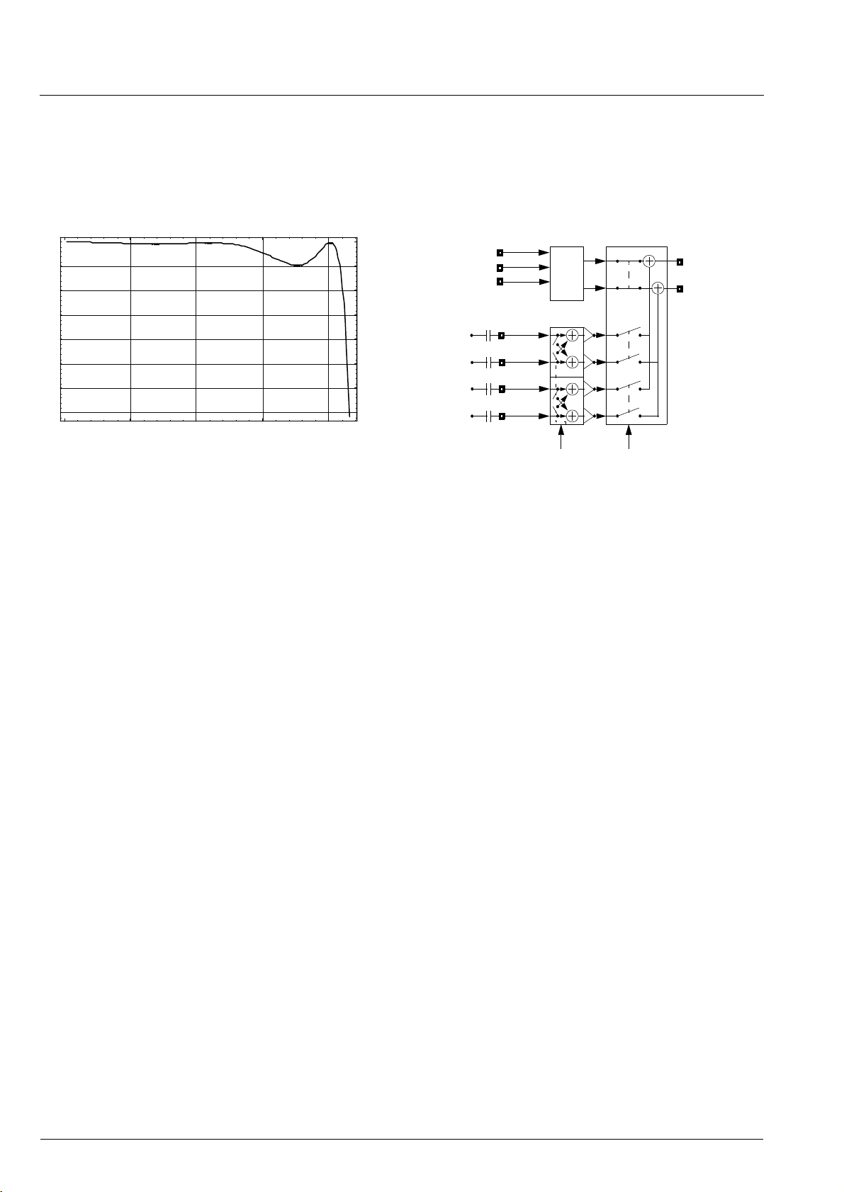
2.2. Interpolation Filter
The interpolation filter increases the sampling rate by a
factor of 8. The characteristic for fs
= 48 kHz is
audio
shown in Fig. 2–3.
0
-0.02
-0.04
-0.06
-0.08
-0.1
-0.12
-0.14
0 5000 10000 15000 20000
Fig. 2–3: 1
→8 Interpolation filter; frequency range:
0...22 kHz
2.3. Variable Sample and Hold
The advantage of this system is that even at low sample frequencies the out-of-band noise is not scaled
down to audible frequencies.
2.4. 3rd-order Noise Shaper and Multibit DAC
The 3rd-order no ise shaper conver ts the oversampled
audio signal into a 5-bit n oise-shap ing signal at a hig h
sampling rate. This tec hnique results in extremely low
quantization noise in the audio band.
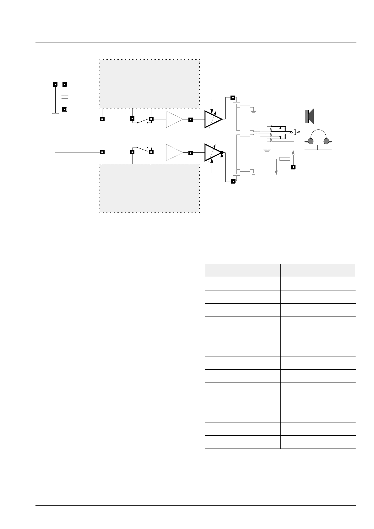
2.6. Input Select and Mixing Matrix
This block is used to switch between or mix the au xiliary inputs and the signals coming from the DAC. A
switch matrix allows to select b etween mono and stereo mode as shown in Fig. 2–4.
FOUTL
FOUTR
INSEL_AUX2
INSEL_AUX1
INSEL_DAC
AUX1L
AUX1R
AUX2L
AUX2R
DAD
DAI
WSI
D/A
24.576 MHz
-
-
-
-
AUX_MS
Fig. 2–4: Switch matrix
Mono mode is realized by adding left and right
channel.
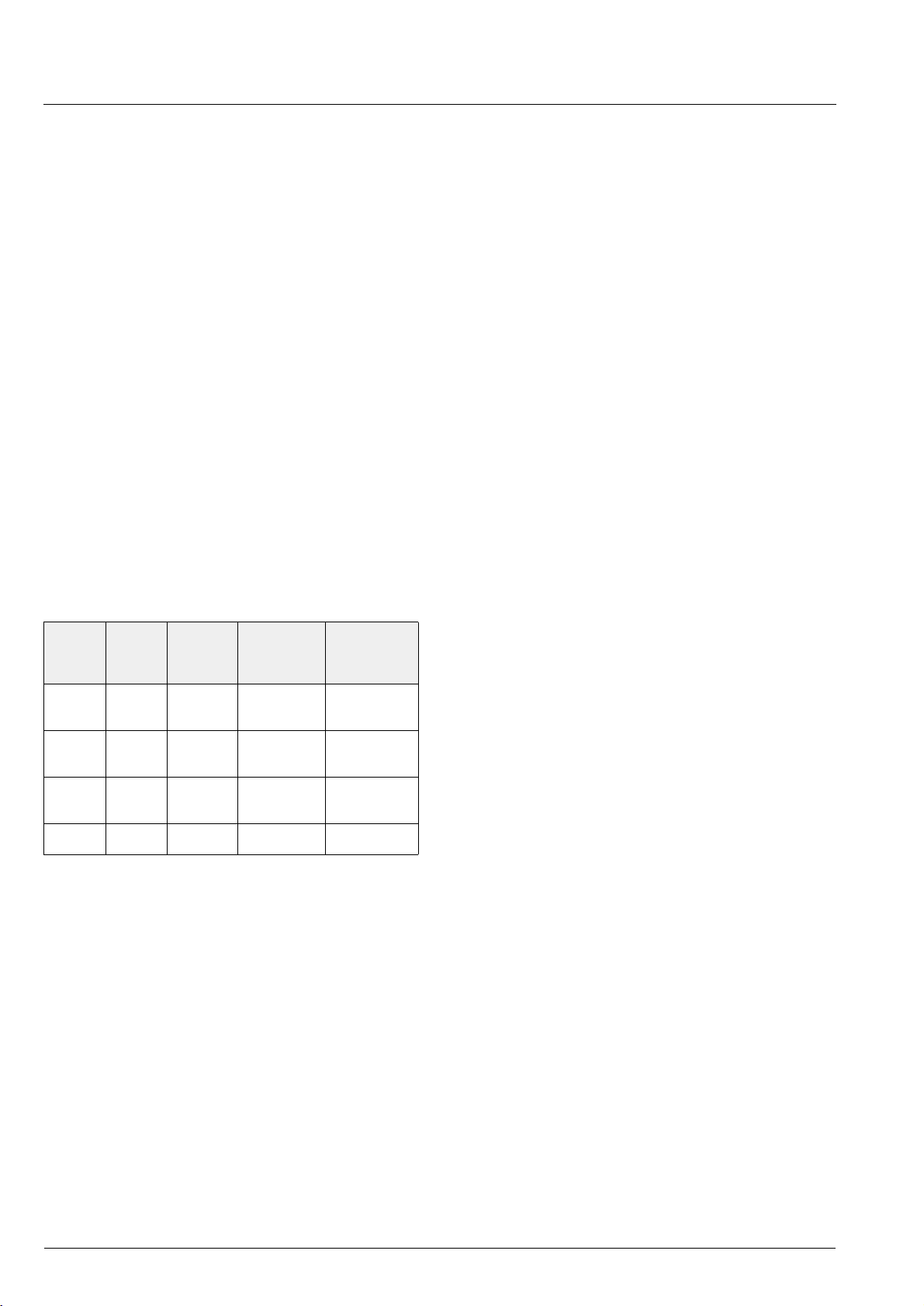
2.7. Postfilter Op Amps, Deemphasis Op Amps,
and Line-Out
This block contains the active components for the analog postfilters and the deemphasis network. The
op amps and all I/O-pins for this block are shown in
Fig. 2–5.
2.5. Analog Low-pass
The analog low-pass is a first or der filter with a cut -off
frequency of approximately 1.4 MHz which removes
the high-frequency components of the noise-shaping
signal.
6 Micronas
Page 7
optional line-out
DAC 3550A
AVSS
from switch matrix
AGNDC
+
µF/100 nF
3.3
VREF
FOUTL
FOUTR
For external components,
see section “Applications”
DEEML
DEEMR
For external components
see section “Applications”
FOPL
FOPR
-
FINL
FINR
-
-
-
,
Fig. 2–5: Postfilter op amps, deemphasis op amps, and line-out
2.8. Analog Volume
Ta ble 2–1: Volume Control
AVOL_R
AVOL_L
OUTL
F
µ
150
F
µ
150
+
47 Ω
47
+
OUTR
1.5 kΩ
Ω
1.5 k
Ω
to µC (HP-switch)
Speaker
32 Ω
16-32 Ω
Headphones
AVDD
IRPA
The analog volume control covers a range from
+18 dB to
−75 dB. The lowest step is the mute posi-
tion.
Step size is split into a 3-dB and a 1.5-dB range:
−75 dB...−54 dB: 3 dB step size
−54 dB...+18 dB: 1.5 dB step size
2.9. Headphone Amplifier
The headphone amplifier output is provided at the
OUTL and OUTR pins connected either to stereo
headphones or a mono loudspeaker. The stereo headphones require external 47-
Ω serial resistors in both
channels. If a loudspeaker is co nnected to these outputs, the power amplifier for the r ight ch annel must be
switched to inverse polarity. In order to optimize the
available power, the source of the two output amplifiers
should be identical, i.e. a monaural signal.
Please note, that if a speaker is connec ted, it should
strictly be connected as shown in Fig. 2–5. Never use
a separate connector for the speaker, because electrostatic discharge could damage the output transistors.
Volume/dB AVOL
18.0 111000
16.5 110111
15.0 110110
13.5 110101
−−
0.0 101100 (default)
−1.5 101011
−−
−
54.0 001000
−57.0 000111
−−
−
75 000001
Mute 000000
Micronas 7
Page 8
DAC 3550A
2.10. Clock System
The advantage of the DAC 3550A clock syste m is that
no external master clock is neede d. Most DACs need
256
× fs
audio
, 384 × fs
, or at least an asynchro-
audio
nous clock.
All internal clocks are generated by a PLL circuit,
which locks to the I
2
S bit clock (CLI). If no I2Sclock is
present, the PLL runs free, and it is guaranteed that
there is always a clock to keep the IC controllable by
2
I
C.
The device can be set to two different modes:
– Standard mode
– MPEG mode
In the standard mode, I
2
C subaddressing is possible
(ADR0, ADR1, ADR2).
MPEG mode always uses ADR3.
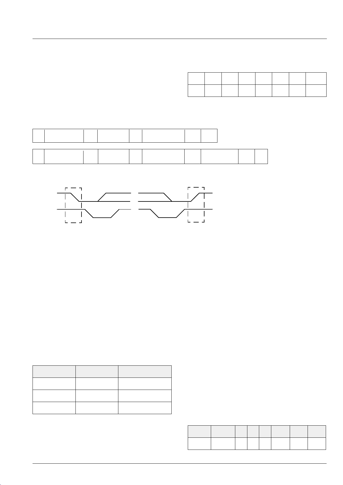
To select the modes, the MCS1/MCS2 pins must be
set according to Table 2–2.
2.10.1. Standard Mode
2
– without I
In standard mode, sample rates from 48 kHz to
32 kHz are handled without I
C
2
C control automati-
cally . T he setting for this range is the default setting.
– with I
2
C
Sample rates below 32 kHz require an I
2
C control to
set the PLL divider. This ensures that even at low
sample rates, the DAC 3550A ru ns at a high clock
rate. This avoids audible effects due to the noiseshaping technique of the DAC 3550A. Sample rate
range is continuous fro m 8 to 50 kHz . The I
2
ting of low sample rates must follow according to
Section 3.6. “Control Registers” on page 15.
An additional mode allows automatic sample rate
detection. In this case, the clock oscillator is
required and must run at frequencies between
13.3 MHz to 17 MHz. This mode, however, does not
suppor t con t inuo us s am ple rates. Only the following
sample rates are allowed:
8 kHz, 11.025 kHz, 12 kHz, 16 kHz, 22.05 kHz,
24 kHz, 32 kHz, 44.1 kHz, 48 kHz
C set-
Table 2–2: Operation Modes
MCS1 MCS2 Mode Sub-
address
00Stan-
dard
01Stan-
dard
10Stan-
dard
1 1 MPEG ADR3 Automatic
ADR0 32–48 kHz
ADR1 32–48 kHz
ADR2 32–48 kHz
Default
Sample
Rate
The sample rate detection allows a tolerance of
±200 ppm at WSI.
If the oscillator is not used for automatic sample rate
detection, it can be used as a gene ral-purpose clock
for the application. The freq uency range in this cas e is
10 MHz to 25 MHz.
2.10.2. MPEG Mode
This mode should be used in conjunction with
MAS 350 7D in MPEG player applications. In this case
a 14.725 M Hz signal is needed to provide a clock for
the MAS 3507D and to allow an automatic sample rate
detection in the DAC 3550A. All MPEG sample rates
from 8 to 48 kHz can be detected. The internal processing and the DAC itself are automatically adjusted
to keep constant performance throughout the entire
range. I
2
C control for sample rate adjustment is not
needed in this case. Regi ster SR_REG[0:2] is locked
to SRC_A; see Section 3.6. “Control Registers” on
page 15.
The MPEG sample rates:
8 kHz, 11.025 kHz, 12 kHz, 16 kHz, 22.05 kHz,
24 kHz, 32 kHz, 44.1 kHz, 48 kHz
As in standard mo de, the s amp le rat e d etec ti on allows
a tolerance of
±200 ppm at WSI.
Subaddressing is not possible in MPEG mode; this
means, in multi-DAC systems, only one DAC 3550A
can run in MPEG mode.
8 Micronas
Page 9
DAC 3550A
s
2.11. I2C Bus Interface
2
The DAC 3550A is equipped with an I
interface. The I
addressing: The I
2
C bus interface uses one level of sub-
2
C bus address is used to address
Cbus slave
the IC. The subaddr ess allows chip select in multi DAC
applications and selects one of the three internal registers. The registers are write-only. The I
2
Cbus chip
The registers of the DAC 3550A have 8- or 16-bit data
size; 16-bit registers a re accessed by wr iting two 8-b it
data words.
A6 A5 A4 A3 A2 A1 A0 R/W
10011010
address is given below.
dev_write = $9A.
1 byte dataS dev_write Ack sub_adr Ack Ack P
8-bit I2C wr i te ac ce ss
S dev_write Ack sub_adr Ack 1 byte data Ack 1 byte data Ack P
=
SDA
SCL
1
S
0
P
W
R
Ack
Nak
S
P
=
=
=
=
=
16-bit I2C write acces
0
1
0
1
Start
Stop
2
Fig. 2–6: I
C bus protocols for write operatio ns
2.12. Registers
In Section 3.6. “Control Registers” on p age 15, a de finition of the DAC 3550A control registe rs is shown. A
hardware reset initializes all control registers to 0. The
automatic chip initialization loads a selected set of registers with the default values given in the table.
All registers are write-only.
The register address is coded by 3 bits (RA1, RA0)
according to Table 2–3.
Table 2–3: I2C Register Address
RA1 RA0 Mnemonics
01SR_REG
10AVOL
2.13. Chip Select
Chip select all ows to c onn ec t u p to four DAC 3550A to
2
C control bus. The chip subaddresses are defined
an I
by the MCS1/MCS2 (Mode and Chip Select) pins. Only
in standard mode, chip select is possible. MPEG mode
always uses chip subaddress 3.
Register address an d chip select are m apped into the
subaddress field in Table 2–4.
2.14. Reduced Feature Mode
2
C control i s not us ed, the I C is in t he default mo de
If I
(see Section 3.6. “Contro l Regi s ters ” on page 15) after
start-up. Default Volume setting is 0 dB and digital
audio input is set to standard I
2
S. Sample rates from
32 kHz to 48 kHz are suppo rted in this mode. App lica tions with no nee d for volume control or analog input
could use this mode.
11GCFG
Ta ble 2–4: I2C Subaddress
The mnemonics used in the DAC 3550A demo software of Micronas are given in the last column.
7 6 5 4 3 2 1 0
MCS2 MCS1 RA1 RA0
Micronas 9
Page 10
DAC 3550A
3. Specifications
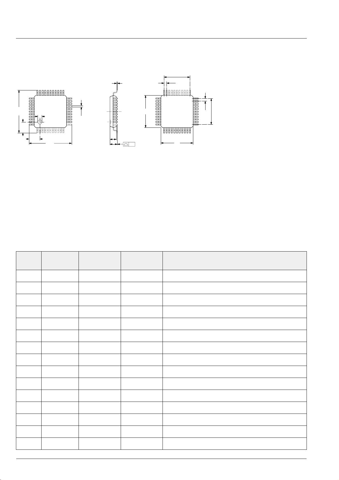
3.1. Outline Dimensions
2333
0.17
10 x 0.8 = 8
0.8
13.2
34
1.75
44
1.75
1.3
1
13.2
22
0.375
12
11
2.0
2.15
0.1
Fig. 3–1:
44-Pin Plastic Metric Quad Flat Package
(PMQFP44)
Weight approximately 0.4 g
Dimensions in mm
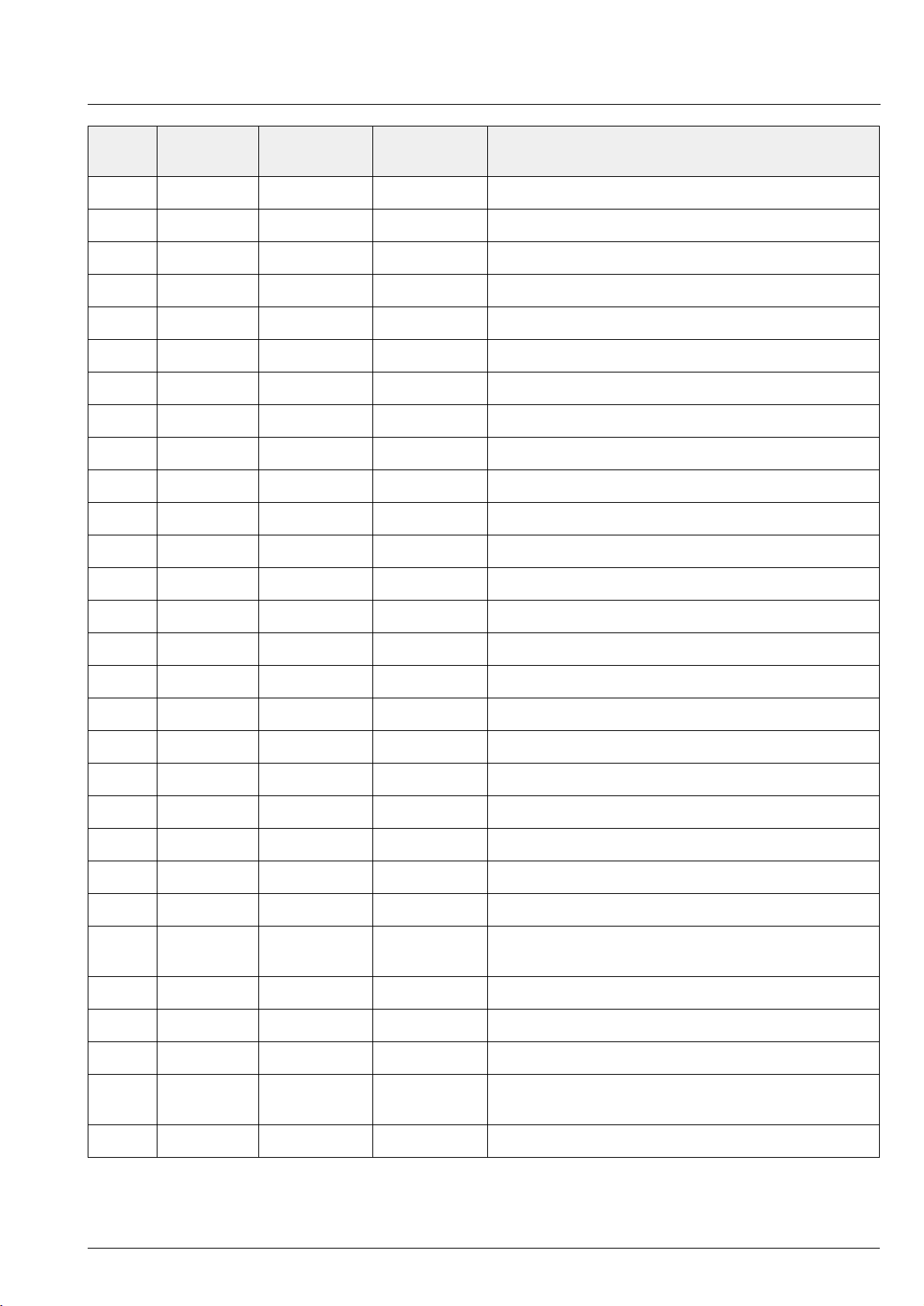
3.2. Pin Connections and Short Descriptions
NC = not connected, leave vacant
LV = if not used, leave vacant
VSS = if not used, connect to VSS
Pin
No.
Pin Name Type Connection
(if not used)
10
10
0.8
10 x 0.8 = 8
D0024/2E
X = obligatory; connect as described in application
diagram
VDD = connect to VDD
Short Description
1 AGNDC IN/OUT X Analog reference Vol tage
2 AVSS1 IN X VSS 1 for audio back-end
3 AVSS0 IN X VSS 0 for audio output amplifiers
4 NC LV Not connected
5 OUTL OUT LV Audio Output: Headphone left or Speaker +
6 NC LV Not connected
7 OUTR OUT LV Audio Output: Headphone right or Speaker
8 NC LV Not connected
9 AVDD0 IN X VDD 0 for audio output amplifiers
10 AVDD1 IN X VDD 1 for audio back-end
11 NC LV Not connected
12 XTI IN X Quartz oscillator pin 1
13 XTO IN/OUT X Quartz oscillator pin 2
14 CLKOUT OUT LV Clock Output
15 SCL IN/OUT LV I
2
C clock
−
10 Micronas
Page 11
DAC 3550A
Pin
No.
Pin Name Type Connection
(if not used)
Short Description
16 SDA IN/OUT LV I2C data
17 VSS IN X Digital VSS
18 VDD IN X Digital VDD
19 MCS1 IN X I
20 MCS2 IN X I
2
C Chip Select 1
2
C Chip Select 2
21 DEECTRL IN VSS Deemphasis on/off Control
22 NC LV Not connected
23 CLI VSS I
24 DAI IN VSS I
25 WSI IN VSS I
2
S Bit Clock
2
S Data
2
S Frame Identification
26 PORQ IN VDD Power-On Reset, active-low
27 TESTEN IN X Test Enable
28 NC LV Not connected
29 AUX2L IN LV AUX2 left input for external analog signals (e.g. tape)
30 AUX2R IN LV AUX2 right input for external analog signals (e.g. tape)
31 AUX1L IN LV AUX1 left input for external analog signals (e.g. FM)
32 AUX1R IN LV AUX1 right input for external analog signals (e.g. FM)
33 NC LV Not connected
34 DEEML OUT LV Deemphasis Network Left
35 DEEMR OUT LV Deemphasis Network Right
36 NC LV Not connected
37 FOUTL OUT X Output to left external filter
38 FOPL IN/OUT X Filter op amp inverting input, left
39 FINL IN/OUT X Input for FOUTL or
filter op amp output (line out)
40 NC LV Not connected
41 FOUTR OUT X Output to right external filter
42 FOPR IN/OUT X Right Filter op amp inverting input
43 FINR IN/OUT X Input for FOUTR or
filter op amp output (line out)
44 VREF IN X Analog reference Ground
Micronas 11
Page 12

DAC 3550A
3.3. Pin Descriptions
3.3.1. Power Supply Pins
The DAC 3550A combines various analog and digital
functions which may be used in different modes. For
optimized performance, major parts have their own
power supply pins. All VSS power supply pins must be
connected.
VDD (18)
VSS (17)
The VDD and VSS power s upply pair are connected
internally with all digital parts of the DAC 3550A.
AVDD0 (9)
AVSS0 (3)
AVDD0 and AVSS0 are separate power supply pins
that are exclusively used for the on-chip headphone/
loudspeaker amplifiers.
AVDD1 (10)
AVSS1 (2)
The AVDD1 and AVSS1 pins supply the analog audio
processing parts, except for the headphone/loudspeaker amplifiers.
FOUTL (37)
FOPL (38)
FINL (39)
FOUTR (41)
FOPR (42)
FINR (43)
Filter op amps are provided in the analog baseband
signal paths. These inverting op amps are freely
accessible for external use by these pins.
The FOUTL/R pins are connected with the buffered
output of the inter nal switch matrix. The FOPL/R-pins
are directly conne cted with the inverting inputs of the
filter op amps. The FINL/R pins are connected with the
outputs of the op amps. The driving capability of the
FOUTL/R pins is not suff icient for standard line output
signals. Only the FINL /R pins are suitable for line output.
OUTL (5)
OUTR (7)
The OUTL/R pins are connec ted to th e inter nal output
amplifiers. They can be used for either stereo headphones or a mono loud sp eaker. The signal of the r ight
channel amplifier can be inverted for mono loudspeaker operation.
3.3.2. Analog Audio Pins AGNDC (1)
Reference for analog audio signals. This pin is used as
reference for the internal op amps. This pin must be
blocked against VREF with a 3.3
Note: The pin has a typical DC-level of 1.5/2.25 V. It
can be used as reference input for external op a mps
when no current load is applied.
VREF (44)
Reference ground for the internal band -gap and biasing circuits. This pi n should be connected to a clea n
ground potential. Any external distortions on this pin
will affect the analog performance of the DAC 3550A.
AUX1L (31)
AUX1R (32)
AUX2L (29)
AUX2R (30)
The AUX pins provide two analog s tereo inputs. Auxiliary input signals, e.g. the output of a conventional
receiver circuit or the outp ut of a tape rec order can b e
connected with these inputs. The inp ut sign als have to
be connected by capacitive coupling.
µF capacitor.
Caution: A short circuit at these pins for more than a
momentary period may result in destruction of the
internal circ uits.
3.3.3. Oscillator and Clock Pins XTI (12)
XTO (13)
The XTI pin is connected to the input of the internal
crystal osci llator, the XTO pin to its output. Both pins
should be directly connected to the crystal and two
ground-connected capacitors (see application diagram).
CLKOUT (14)
The CLKOUT pin provides a buffered output of the
crystal oscillator.
Caution: Power dissipation limit may be exceeded in
case of short to VSS or VDD.
CLI (23)
DAI (24)
WSI (25)
These three pins are inputs for the digital audio data
DAI, frame indication signal WSI, and bit clock CLI.
The digital audio data is transmi tted in an I
ble format. Audio word lengths of 16 and 32 bits are
supported, as well as SONY and Philips I
2
S-compati-
2
Sprotocol.
SCL (15)
SDA (16)
SCL (serial clock) and SDA (serial data) provide the
connection to the serial control interface (I
12 Micronas
2
C).
Page 13
DAC 3550A
3.3.4. Other Pins TESTEN (27)
Test enable. This pi n is for test purposes only and must
always be connected to VSS.
PORQ (26)
This pin may be used to reset the chip. If not used, this
pin must be connected to VDD.
DEEML (34)
DEEMR (35)
These pins connect an external analog deemphasis
network to the signal path in the analog back-end. This
connection can be switched on and off by an internal
switch which is controlled either by I
2
C or the
DEECTRL-pin.
DEECTRL (21)
2
If no I
C-control is used , deemphas is can be switched
on and off with this pin.
MCS1 (19)
MCS2 (20)
Mode select pins to select MPEG, Standard Mode, and
2
C subaddress.
I
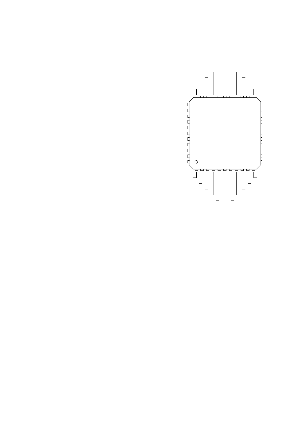
3.4. Pin Configuration
AUX2L
AUX2R
AUX1L
AUX1R
NC
33 32 31 30 29 28 27 26 25 24 23
34
DEEML
DEEMR
35
NC
36
FOUTL
37
FOPL
38
FINL
NC
FOUTR
FOPR
FINR
VREF
AGNDC
39
40
41
42
43
44
AVSS1
DAC 3550A
1234567891011
AVSS0
NC
OUTL
NC
NC
TESTEN
PORQ
NC
OUTR
WSI
DAI
AVDD1
AVDD0
CLI
22
21
20
19
18
17
16
15
14
13
12
NC
NC
DEECTRL
MCS2
MCS1
VDD
VSS
SDA
SCL
CLKOUT
XTO
XTI
Fig. 3–2: 44-pin PMQFP pa ckage
Micronas 13
Page 14

DAC 3550A
Fig. 3–3: Input/Output Pins SDA, SCL
N
VSS
VDD
Fig. 3–4: Input Pins DAI, WSI, PORQ, CLI
Fig. 3–5: Output Pin CLKOUT
P
VDD
N
VSS
Fig. 3–6: Pins FINR, FOPR, FINL, FOPL,
DEEML, DEEMR
AGNDC
FOPn
FINn
FOUTn
ext. filter network
DEEM
(DEEMCTRL)
Fig. 3–7: Pins AGNDC, VREF
125 k
AVSS0/1
AGNDC
VREF
3.5. Pin Circuits
FOUTn
AGNDC
Fig. 3–8: Output Pins FOUTL, FOUTR
XTO
500 k
XTI
Fig. 3–9: Input/Output Pins XTI, XTO
AUXnL
sel/nonsel
AGNDC
mono/stereo
AGNDC
mono/stereo
AUXnR
sel/nonsel
Fig. 3–10: Input Pins AUX1R, AUX1L, AUX2R,
AUX2L, AGNDC
AGNDC
OUTn
Fig. 3–11: Output Pins OUTL, OUTR
VDD
14 Micronas
VSS
Fig. 3–12: Input Pins MCS1, MCS2, DEECTRL
Page 15

3.6. Control Registers
DAC 3550A
I2C Subaddress
(hex)
Number
of Bits
Mode Function Default
SAMPLE RATE CONTROL SR_REG
01 8 w sample rate control
bit[7:5] not used, set to 0
bit[4] L/R-bit
0(WSI = 0
1(WSI = 0 → right channel)
bit[3] Delay-Bit
0 No Delay
1 1 bit Delay
bit[2:0] sample rate control
000 32
001 26
010 20
011 14
100 10
101 8
2)
autoselect
11x
ANALOG VOLUME AVOL
→ left channel)
−48 kHz
−32 kHz
−26 kHz
−20 kHz
−14 kHz
−10 kHz
Name
Values
(hex)
0H
1)
1)
LR_SEL
SP_SEL
SRC_48
SRC_32
SRC_24
SRC_16
SRC_12
SRC_8
SRC_A
02 16 w audio volume control
bit[15] not used, set to 0
bit[14] deemphasis on/off
0 deemphasis off
1 deemphasis on
bit[13:8] analog audio volume level left:
000000 mute
000001
101100 +0 dB (default)
111000 +18 dB
bit[7:6] not used, set to 0
bit[5:0] analog audio volume level right
000000 mute
000001
101100 +0 dB (default)
111000 +18 dB
1)
see Fig. 2–1 and Fig. 2–2 on page
2)
don’t care
5
2C2CH
DEEM
AVOL_L
−75 dB
AVOL_R
−75 dB
Micronas 15
Page 16

DAC 3550A
I2C Subaddress
(hex)
Number
of Bits
Mode Function Default
Global Configuration GCFG
03 8 w global configuration
bit[7] not used, set to 0
bit[6] select 3V-5 V mode
03V
15V
bit[5] power-mode
0normal
1low power
bit[4] AUX2 select
0AUX2 off
1AUX2 on
bit[3] AUX1 select
0AUX1 off
1AUX1 on
bit[2] DAC select
0DAC off
1 DAC on (default)
Name
Values
(hex)
4H
SEL_53V
PWMD
INSEL_AUX2
INSEL_AUX1
INSEL_DAC
bit[1] aux-mono/stereo
0stereo
1 mono
bit[0] invert right power amplifier
0 not inverted
1inverted
AUX_MS
IRPA
16 Micronas
Page 17
3.7. Electrical Characteristics
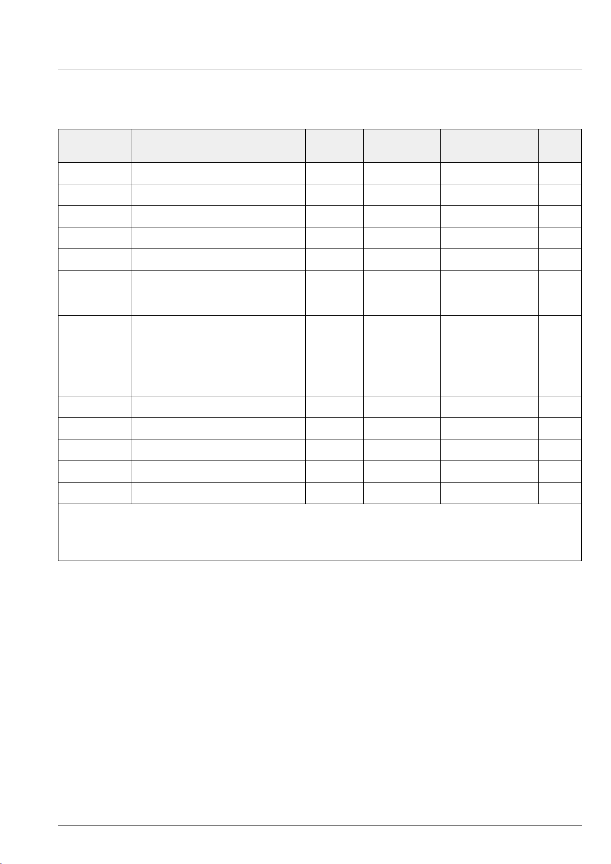
3.7.1. Absolute Maximum Ratings
DAC 3550A
Symbol Parameter Pin
Name
T
A
T
P
V
V
V
S
max
SUPA
SUPD
Idig1
Ambient Operating Temperature
Storage Temperature −40 125 °C
Power Dissipation 500 mW
Analog Supply Voltage
2)
Digital Supply Voltage VDD −0.3 6 V
Input Voltage, digital inputs MCS1,
1)
AVDD0/1 −0.3 6 V
MCS2,
DEECTRL
V
Idig2
Input Voltage, digital inputs WSI,
CLI,
DAI,
PORQ,
SCL,
SDA
I
V
Idig
Iana
Input Current, all digital inputs −5+5 mA
Input Voltage, all analog inputs −0.3 V
Min. Max. Unit
070 °C
−0.3 V
+ 0.3 V
SUPD
−0.3 6 V
+ 0.3 V
SUPA
I
Iana
I
Oaudio
I
Odig
1)
=standard temperature range, DAC 3550A tested in extended temperature range on request
2)
Both have to be connected together!
3)
These pins are NOT short-circuit proof!
4)
Total chip power dissipation must not exceed absolute maximum rating
Input Current, all analog inputs −5+5 mA
Output Current, audio output
Output Current, all digital outputs
3)
OUTL/R −0.2 0.2 A
4)
−10 10 mA
Stresses beyond those listed in the “Absolute Maximum Ratings” may cause per m anent damage to the device. This
is a stress rating onl y. Functional operation of the device at these or any ot her c onditions beyond those indi cated in
the “Rec ommended O perating Conditio ns/Characteris tics” of this s pecification is not implied. Exposure to absolute
maximum ratings conditions for extended periods may affect device reliability.
Micronas 17
Page 18
DAC 3550A
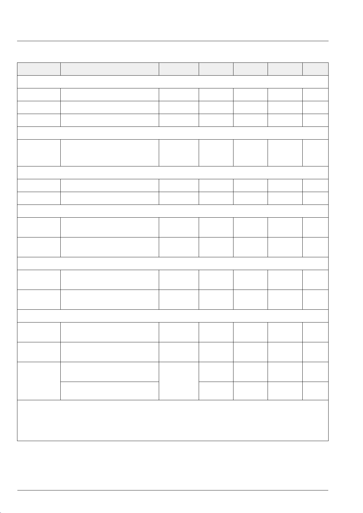
3.7.2. Recommended Operating Conditions
Symbol Parameter Pin Name Min. Typ. Max. Unit
Temperature Ranges and Supply Voltages
T
A
V
SUPA1
Ambient Temperature Range
Analog Audio Supply Voltage AVDD0/1 3.0
1)
070°C
2)
3.3 5.5 V
V
SUPD
Digital Supply Voltage VDD 2.7 3.3 5.5 V
Relative Supply Voltages
V
SUPA
Analog Audio Supply Voltage in
relation to the Digital Supply Volt-
age
Analog Reference
C
AGNDC1
C
AGNDC2
Analog Reference Capacitor AGNDC 1.0 3.3 µF
Analog Reference Capacitor AGNDC 10 nF
Analog Audio Inputs
V
AI
Analog Input Voltage AC,
SEL_53V = 0
V
AI
Analog Input Voltage AC,
SEL_53V = 1
Analog Filter Input and Output
Z
AFLO
Z
AFLI
Analog Filter Load Output
Analog Filter Load Input
AVDD0/1 V
SUPD
5.5 V
−0.25 V
AUXnL/R
AUXnL/R
4)
4)
FOUTL/R 7.5
FINL/R 5.0
3)
3)
0.35 0.7 V
0.525 1.05 V
rms
rms
kΩ
6
pF
kΩ
7.5
pF
Analog Audio Ou tput
Z
LO
Audio Line Output
5)
FINL/R 10
(680 Ω Series Resistor required)
Z
AOL_HP
Z
AOL_SP
Analog Output Load HP
(47
Ω Series Resistor required)
OUTL/R 32
400
Analog Output Load SP (bridged) OUTL/R 32
50
Analog Output Load SP (Stereo) 16
100
1)
=standard temperature range, DAC 3550A tested in extended temperature range on request
2)
typically operable down to 2.7 V, without loss in performance
3)
n = 1 or 2
4)
Please refer to Section 4.2. “Recommended Low-Pass Filters for Analog Outputs” on page 25.
5)
Please refer to Section 4.1. “Line Output Details” on page 25.
1.0
k
nF
Ω
pF
Ω
pF
Ω
pF
Ω
18 Micronas
Page 19

DAC 3550A
Symbol Parameter Pin Name Min. Typ. Max. Unit
I2C Input
f
I2C1
f
I2C2
I2C Clock Frequency, I2S active SCL 400 kHz
I2C Clock Frequency, I2S inactive 100 kHz
Digital Inputs
V
IH
Input High Voltage CLI,
WSI,
0.5×
VDD
DAI,
V
IL
Input Low Voltage 0.2×
PORQ,
SCL,
SDA
Quartz Characteristics
F
P
R
EQ
C
0
Load Resonance Frequency
= 20 pF
at C
l
Equivalent Series Resistance 12 30 Ω
Shunt (parallel) Capacitance 3 5 pF
13.3 14.725 17 MHz
Load at CLKOUT Output
C
load
1)
=standard temperature range, DAC 3550A tested in extended temperature range on request
2)
typically operable down to 2.7 V, without loss in performance
3)
n = 1 or 2
4)
Please refer to Section 4.2. “Recommended Low-Pass Filters for Analog Outputs” on page 25.
5)
Please refer to Section 4.1. “Line Output Details” on page 25.
Capacitance CLKOUT 0 50 pF
V
V
VDD
Micronas 19
Page 20
DAC 3550A
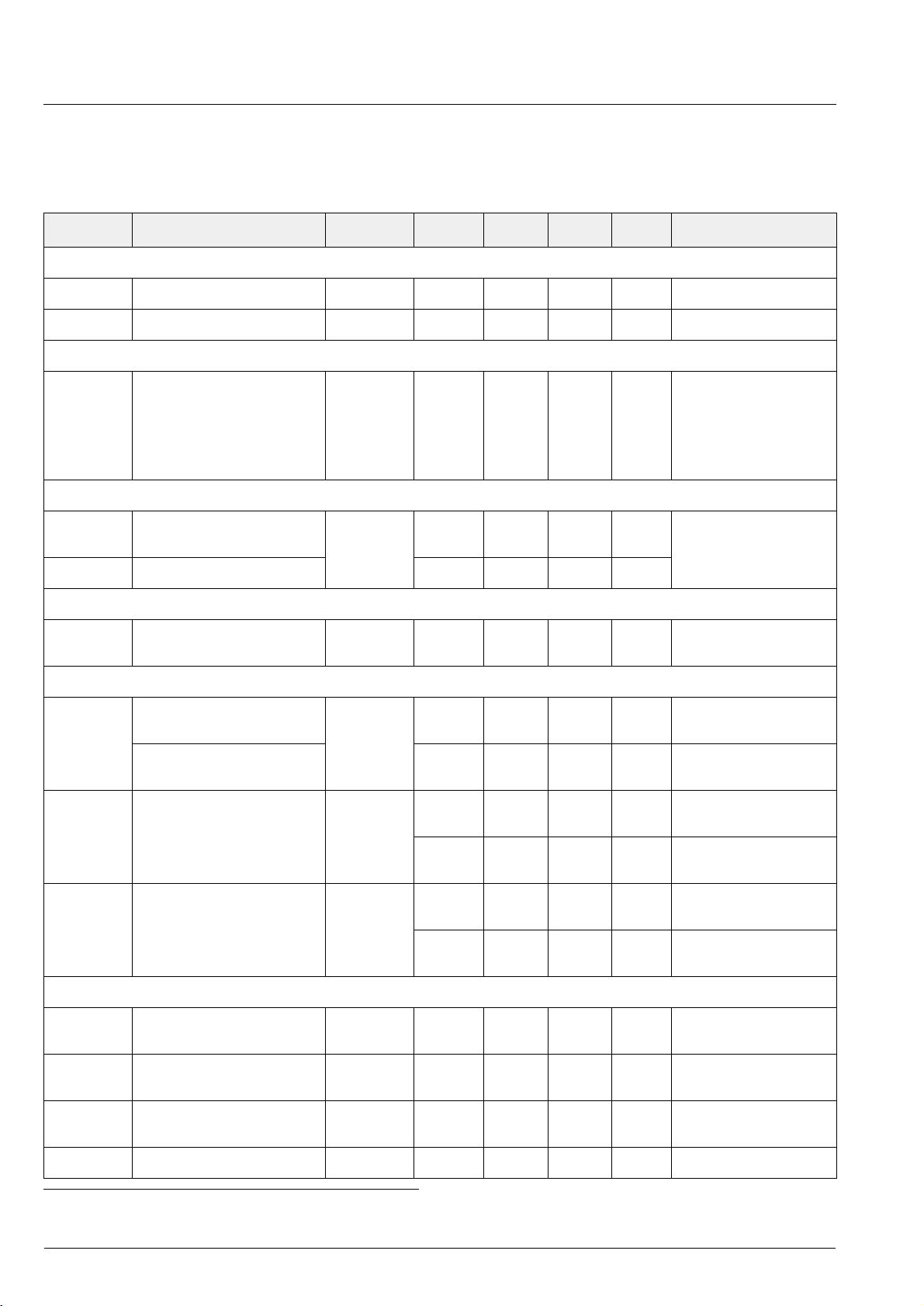
3.7.3. Characteristics
= 0 to 70 °C*, V
At T
A
= 2.7 to 5.5 V, V
SUPD
= 3.0 to 5.5 V; typical values at TJ=27°C, V
SUPA
SUPD=VSUPA
quartz frequency = 14.725 MHz, duty cycle = 50 %, positive current flows into the IC
Symbol Parameter Pin Name Min. Typ. Max. Unit Test Conditions
Digital Supply
I
VDD
I
VDD
Digital Input Pin
I
I
Digital Output Pin – Clock Out
V
OH
V
OL
2
I
C Bus
Current Consumption VDD 5 mA V
Current Consumption VDD 8 mA V
– Leakage
Input Leakage Current CLI, WSI,
DAI,
TESTEN,
PORQ,
DEECTRL,
MCS1/2
Output High Voltage CLKOUT V
SUPD
− 0.3
Output Low Voltage 0.3 V
±1 µAV
V no load at output
SUPD
SUPD
GND
=3 V
=5 V
≤ VI ≤ V
=3.3V,
SUP
R
on
Output Impedance SCL, SDA 60 Ω I
Analog Supply
I
AVDD
Current Consumption
Analog Audio, SEL_53V = 0
SEL_53V = 1 11
PSRR
AA
Power Supply Rejection
Ratio for Analog Audio
Output
PSRR
LO
Power Supply Rejection
Ratio for Line Output
Reference Frequency Generation
V
DCXTI
C
LI
DC Voltage at Oscillator
Pins
Input Capacitance at
Oscillator Pin
AVDD0/1 8
1.5
11 mA
mA
15 mA
AVDD0/1,
2
50 dB 1 kHz sine at
mA
OUTL/R
20 dB ≤ 100 kHz sine at
AVDD0/1,
50 dB 1 kHz sine at
FINL/R
40 dB ≤ 100 kHz sine at
XTI/O 0.5 *
V
SUPA
V
XTI/O 3 pF
=5mA,
load
=2.7V
V
SUPD
PWMD = 0, Mute
PWMD = 1, Mute
PWMD = 0, Mute
PWMD = 1, Mute
100 mV
100 mV
100 mV
100 mV
rms
rms
rms
rms
Vxtalout Voltage Swing at Oscillator
Pins, pp
Oscillator Start-Up Time 50 ms AV
XTI/O 60 100 %
VSUP A
DD/VDD
≥ 2.5 V
* =standard temperature range, DAC 3550A tested in extended temperature range on request
20 Micronas
Page 21

DAC 3550A
Symbol Parameter Pin Name Min. Typ. Max. Unit Test Conditions
Analog Audio
V
AO
Analog Output Voltage AC OUTL/R,
FOUTL/R,
FINL/R
0.65 0.7 0.75 V
rms
SEL_53V = 0,
> 5 kΩ,
R
L
Analog Gain = 0 dB
Input = 0 dBFS digital
1.0 1.05 1.1 V
G
AUX
P
HP
Gain from Au xiliary Inputs to
Line Outputs
AUXnL/R,
FINL/R
−0.5 0 0.5 dB f = 1 kHz, sine wave,
Output Power (Headphone) OUTL/R 5 mW SEL_53V = 0,
rms
SEL_53V = 1
RL>5kΩ
rms
= 32 Ω,
L
to AUXnL/R
0.5 V
R
Analog Gain = +3 dB,
distortion < 1%,
external 47 Ω series
resistor required
12 mW SEL_53V = 1
P
SP
Output Power (Speaker) OUTL/R 120 mW RL = 32 Ω (bridged),
Analog Gain = +3 dB,
distortion < 10%,
SEL_53V = 0, IRPA = 1
280 mW SEL_53V = 1
G
AO
Analog Output Gain
Setting Range
OUTL/R −75 18 dB
dG
dG
E
GA1
E
GA2
E
GA3
E
dGA
SNR
AO1
AO2
AUX
Analog Output Gain
Step Size
Analog Output Gain
Step Size
OUTL/R 3.0 dB Analog Gain:
−75 dB...−54 dB
OUTL/R 1.5 dB Analog Gain:
−54 dB...+18 dB
Analog Output Gain Error OUTL/R −22dB−46.5 dB≥Analog Gain
≥−54 dB
Analog Output Gain Error OUTL/R −11dB−40.5 dB≥Analog Gain
≥−45 dB
Analog Output Gain Error OUTL/R −0.5 0.5 dB +18 dB≥Analog Gain
≥−39 dB
Analog Output Gain
Step Size Error
Signal-to-Noise Ratio from
Analog Input to Line Output
Signal-to-Noise Ratio from
Analog Input to Headphone
Output
OUTL/R −0.5 0.5 dB +18 dB≥Analog Gain
≥−48 dB
AUXn,
FINL/R
AUXn,
OUTn
98 dB SEL_53V = 0:
−40 dB below
input
0.7 V
rms
93 dB
Analog Gain = 0 dB,
BW =20 Hz...20 kHz
unweighted
Micronas 21
Page 22

DAC 3550A
Symbol Parameter Pin Name Min. Typ. Max. Unit Test Conditions
SNR
SNR
1
Signal-to-Noise Ratio OUTL/R 89 91 dB RL≥ 32 Ω
(external 47 Ω series
resistor required)
BW =20Hz...0.5fs
unweighted,
Analog Gain = 0 dB,
Input =
FINL/R 90 92 dB R
R
BW etc. as above
16 bit I
94 dB 32 bit I
96 dB 16 bit I
98 dB 32 bit I
103 dBA 32 bit I
2
Signal-to-Noise Ratio OUTL/R 58 62 dB RL≥ 32 Ω (external
47 Ω series resistor
−20 dBFS
≥ 5kΩ,
L
≥ 612 Ω
dec
2
S, SEL_53V = 0
2
S, SEL_53V = 0
2
S, SEL_53V = 1
2
S, SEL_53V = 1
2
S, SEL_53V = 1
required)
BW = 20 Hz..0.5 fs
unweighted
Analog Gain=
Input =
−40.5dB,
−3dBFS
Lev
R
D/A
A
D/A
BW
THD
THD
THD
Mute
AUX
ALO
DLO
HP
Mute Level OUT L/R −110 dBV BW = 20 Hz...22 kHz
unweighted, no digital
input signal,
Analog Gain = Mute
D/A Pass Band Ripple OUTL/R,
FOUTL/R
−0.1 dB 0...0.446 fs
(no external filters
used)
D/A Stop Band Attenuation 40 dB 0.55...7.533 fs
(no external filters
used)
Bandwidth for
Auxiliary I nputs
Total Harmonic Distortion
from Auxiliary Inputs to
Line Outputs
Total Harmonic Distortion
(D/A converter to Line
Output)
Total Harmonic Distortion
(Headphone)
AUXnL/R,
FINL/R
AUXnL/R,
FINL/R
760 kHz (no external filters
used)
0.01 % BW = 20 Hz...22 kHz,
unweighted,
> 5 kΩ
R
L
Input 1 kHz at 0.5 V
R
≥ 612 Ω
dec
FINL/R 0.01 % BW = 20 Hz...0.5 fs,
unweighted,
>5kΩ
R
L
Input 1 kHz at
R
≥ 612 Ω
dec
−3dBFS
OUTL/R 0.05 % BW = 20 Hz...0.5 fs,
unweighted, RL≥ 32 Ω
(47 Ω series resistor
required),
Analog Gain = 0 dB,
Input 1 kHz at
−3dBFS
rms
22 Micronas
Page 23

DAC 3550A
Symbol Parameter Pin Name Min. Typ. Max. Unit Test Conditions
THD
SP
XTALK
XTALK
XTALK
Total Harmonic Distortion
(Speaker)
Cross-Talk
LO
Left/Right Channel
(Line Output)
Crosstalk
HP
Left/Right Channel
(Headphone)
Crosstalk betwee n
2
Input Signal Pairs
OUTL/R 0.5 % BW = 20 Hz...0.5 fs,
unweighted, RL≥ 32 Ω
(speaker bridged),
Analog Gain = 0 dB,
−3dBFS
−3 dBFS or
to AUXnL/R
AUXnL/R,
FOUTL/R,
FINL/R
Input 1 kHz at
−70 −80 dB f = 1 kHz, sine wave,
RL>7.5kΩ
Analog Gain = 0 dB,
Input =
0.5 V
rms
OUTL/R −70 −80 dB f = 1 kHz, sine wave,
OUTL/R: RL ≥ 32 Ω
(47 Ω series resistor
required)
Analog Gain = 0 dB,
−3 dBFS or
Input =
0.5 V
to AUXnL/R
rms
AUXnL/R −70 −80 dB f = 1 kHz, sine wave,
FOUTL/R: R
OUTL/R: RL ≥ 32 Ω
> 7.5 kΩ
L
(47 Ω series resistor
required)
Analog Gain = 0 dB,
−3 dBFS and
Input =
0.5 V
to AUXnL/R
rms
V
AGNDC
Analog Refe rence Voltage AGNDC 1.5 V SEL_53V = 0
>> 10 MΩ,
R
L
referred to VREF
2.25 V SEL_53V = 1
R
>> 10 MΩ,
L
referred to VREF
Micronas 23
Page 24
DAC 3550A
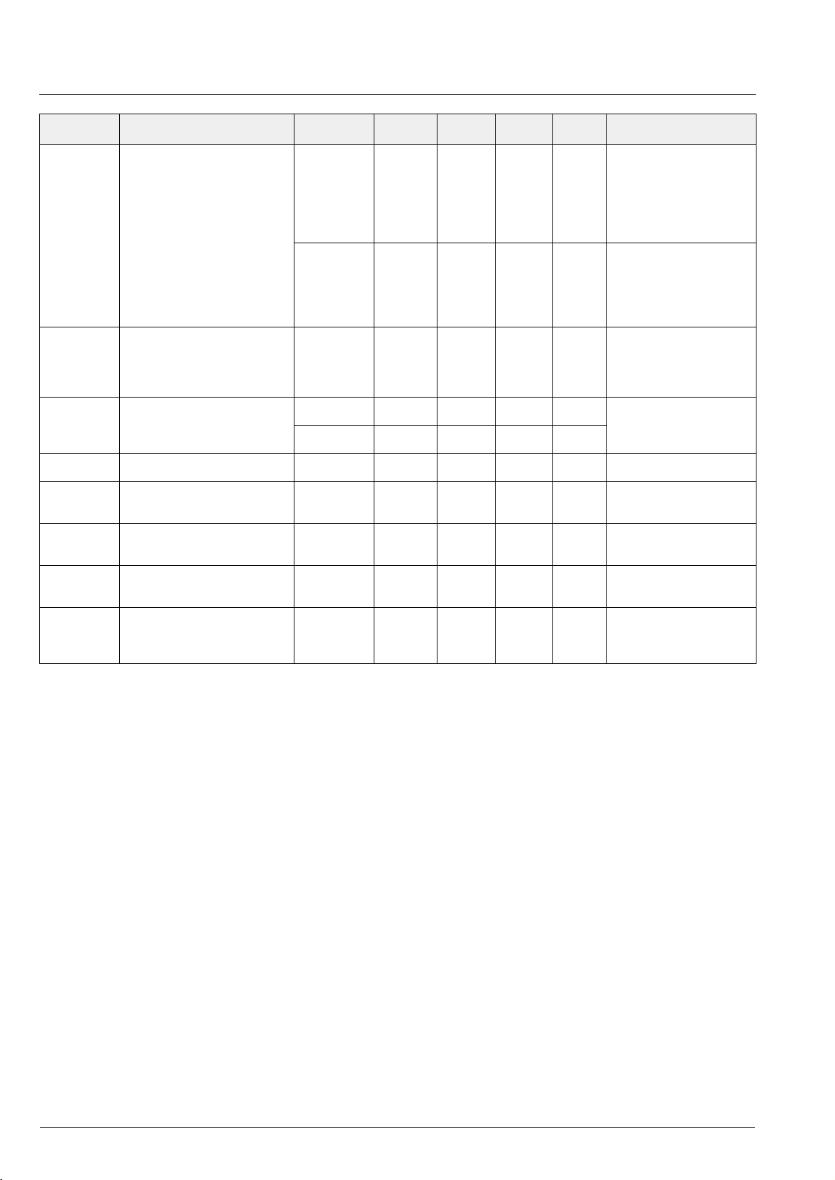
Symbol Parameter Pin Name Min. Typ. Max. Unit Test Conditions
R
IAUX
R
OOUT
R
OFILT
V
OffI
V
OffO
V
OffFO
Input Resistance at
Input Pins
AUXnL/R 12.1
11.6
15 17.9
19.0
kΩ
kΩ
TJ = 27 °C
TA = 0 to 70 °C
1)
Input selected,
PWMD = 0
± 10 µA,
i =
referred to VREF
24.2
23.3
30 35.8
37.9
kΩ
kΩ
= 27 °C
T
J
TA = 0 to 70 °C
1)
Input not selected
i = ± 10 µA,
referred to VREF
Output Resistance at
Output Pins
OUTL/R 700 Ω TJ = 27 °C
PWMD = 1
± 200 µA,
i =
referred to VREF
Output Resistance of
Filter Pins
FINL 15 kΩ PWMD = 1, Mute
i = ± 10 µA,
referred to VREFFINR 11.25 kΩ
Offset Voltage at Input Pins AUXnL/R −20 20 mV referred to AGNDC
Offset Voltage at
Output Pins
Offset Voltage at
Filter Output Pins
OUTL/R −10 10 mV Mute
referred to AGNDC
FOUTL/R −20 20 mV PWMD = 0,
referred to AGNDC
V
dV
OffFI
DCPD
Offset Voltage at
Filter Input Pins
Difference of DC Voltage at
Output Pins after Back-end
Low Power Sequence
FINL/R −20 20 mV PWMD = 0,
referred to AGNDC
OUTL/R −10 10 mV Analog Gain = Mute,
PWMD switched from 0
to 1
24 Micronas
Page 25

DAC 3550A
4. Applications
4.1. Line Output Details
R
dec
R
FINL(R)
AVSS
C
line
in
Fig. 4–1: Use of FINL/R as Line Outputs
Table 4–1: Load at FINL/R when used as Line Output
for external amplifier
Filter Order R
dec
R
in
1st, 2nd, 3rd 680 Ω > 10 kΩ
R
:Resistor used for decoupling C
dec
line
from
FINL(R) to achieve stability
C
: Capacitive load according to e.g. cable,
line
amplifier
R
: Input resistance of amplifier
in
2nd-order
11 kΩ
1.0 nF
AVSS
FOUTL(R)
11 kΩ
220 pF11 kΩ
FINL(R)FOPL(R)
-
Fig. 4–3: 2nd-order low-pass filter
Ta ble 4–3: Attenuation of 2nd-order low-pass filter
Frequency Gain
24 kHz
30 kHz
3rd-order
−1.5 dB
−3.0 dB
15 kΩ
4.2. Recommended Low-Pass Filters for Analog Outputs
FOUTL(R)
*
1st-order
15 kΩ
330 pF
15 kΩ
FINL(R)FOPL(R)
-
Fig. 4–2: 1st-order low-pass filter
Table 4–2: Attenuation of 1st-order low-pass filter
Frequency Gain
24 kHz
30 kHz
−2.2 dB
−3.0 dB
120 pF
FINL(R)FOPL(R)
FOUTL(R)
7.5 kΩ
7.5 k
AVSS
Ω 7.5 kΩ
1.8 nF1.8 nF
-
Fig. 4–4: 3rd-order low-pass filter
Ta ble 4–4: Attenuation of 3rd-order low-pass filter
Frequency Gain
18 kHz 0.17 dB
24 kHz
30 kHz
−0.23 dB
−3.00 dB
* without deemphasis circuit
Micronas 25
Page 26
DAC 3550A
-
FINL(R)FOPL(R)
FOUTL(R)
R3
C3R2 R4
C2C1
R1
AVSS
R5 C4
DEEML(R)
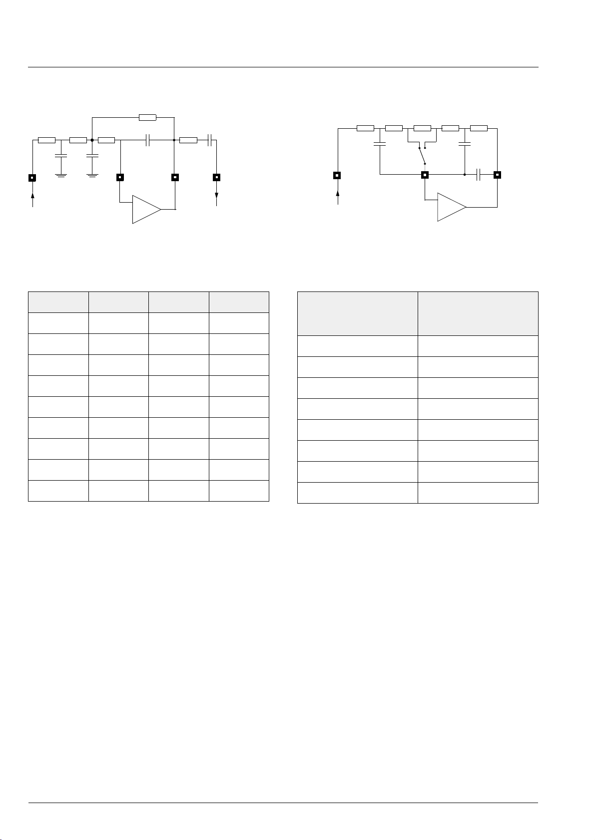
4.3. Recommendations for Filters and Deemphasis
Fig. 4–5: General circuit schem ati c
Table 4–5: Resistor and Capacitor values
1st order 2nd order 3rd order
R1 (k
Ω)0 7.5
C1 (pF) open 560
R2 (k
Ω)18117.5
4.4. Recommendations for MegaBass Filter without Deemphasis plus 1st-order low-pass
R4R2 R3
C2
C3
-
FOUTL(R)
R1 R5
C1
ON OFF
FOPL(R)
Fig. 4–6: General circuit schematic
Table 4–6: Resistor and Capacitor values
DC-Gain = 10 dB
fc1 = 100 Hz
fc2 = 330 Hz
R1 (k
Ω)13
C1 (nF) 47
FINL(R)
C2 (pF) open 1000 270
R3 (k
Ω)181115
C3 (pF) 180 180 82
R4 (k
Ω) 0 11 7.5
R5 (k
Ω)182222
C4 (nF) 1.8 1.0 1.0
R2 (k
Ω)0
R3 (k
Ω)15
R4 (k
Ω)15
R5 (k
Ω)13
C2 (nF) 47
C3 (pF) 180
26 Micronas
Page 27
DAC 3550A
4.5. Power-up/down Sequence
In order to get a click-free power-up/down character istic, it is recommended to use the following sequences:
4.5.1. Power-up Sequence
1. Start VDD from 0 to +3.3 V and start AVDD0/1 from
0 to +3.3 V/+5 V. AVDD should not ramp up faster
than VDD.
2. Release PORQ from 0 to AVDD0/1.
3. Send I2C: volume, input select, speaker, ... optional.
4. Start I2S data.
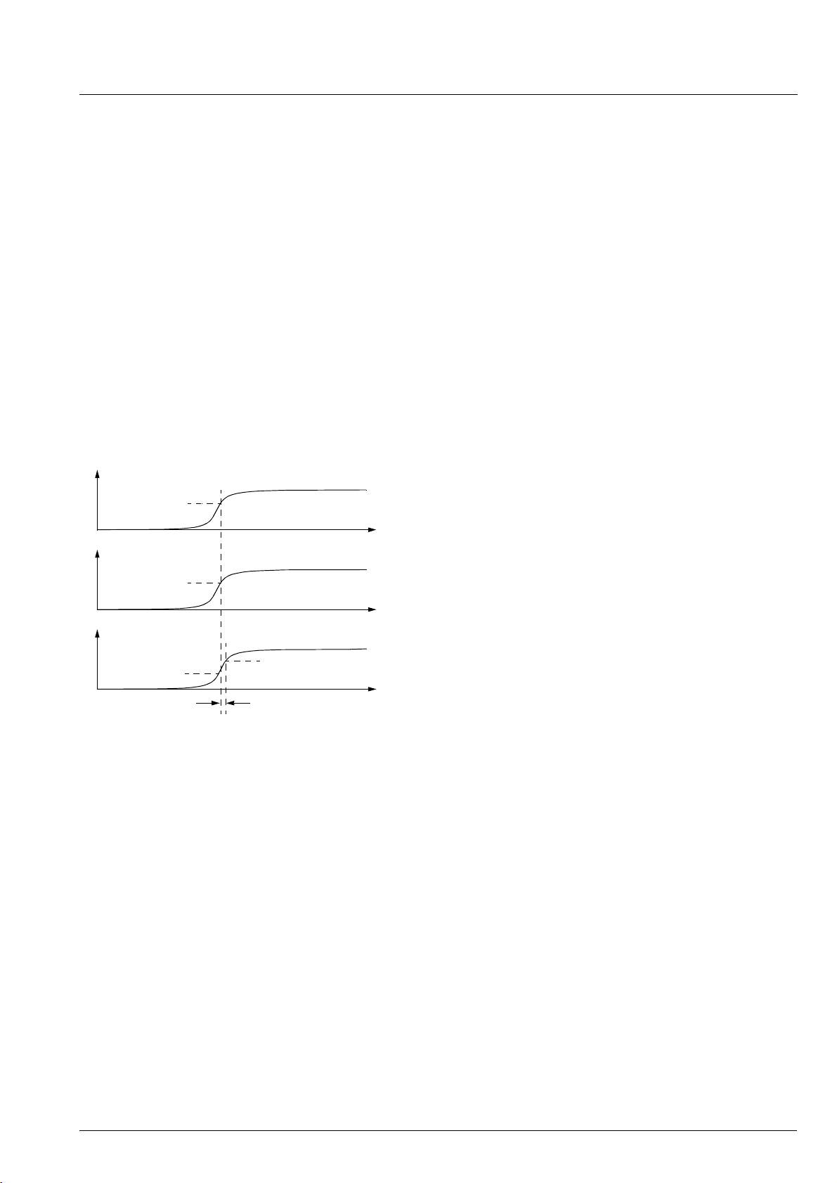
The most important point is: PORQ has to ramp up
after AVDD0/1, simply by using a 10-k
Ω pull-up resis-
tor to AVDD0/1 and a 2.2-nF capacitor to ground. No
further control on PORQ is needed.
VDD
≥90% VDD
4.5.2. Power-down Sequence
1. Stop I2S data.
2. Send I2C: LOW PO WER.
3. Switch VDD, AVDD0/1 to 0.
≥90% AVDD
<0.2
×VDD
<30 m s
Fig. 4–7: Power-up sequence
AVDD
PORQ
0.7×AVDD
Micronas 27
Page 28

28 Micronas
Fig. 4–8: Application circuit schematic 1: Standard application with analog deemphasis. Oscillator not needed.
4.6. Typical Applications
A
n
DAC 3550A
Page 29

Micronas 29
Fig. 4–9: Application circuit schematic 2: MPEG application with analog Megabass and 14.725 MHz crystal
A
n
A
DAC 3550A
Page 30
DAC 3550A
demand signal
Host
(PC, Controller)
ROM, CD-ROM,
RAM, Flash Mem. ..
MPEG clock
MPEG bit stream
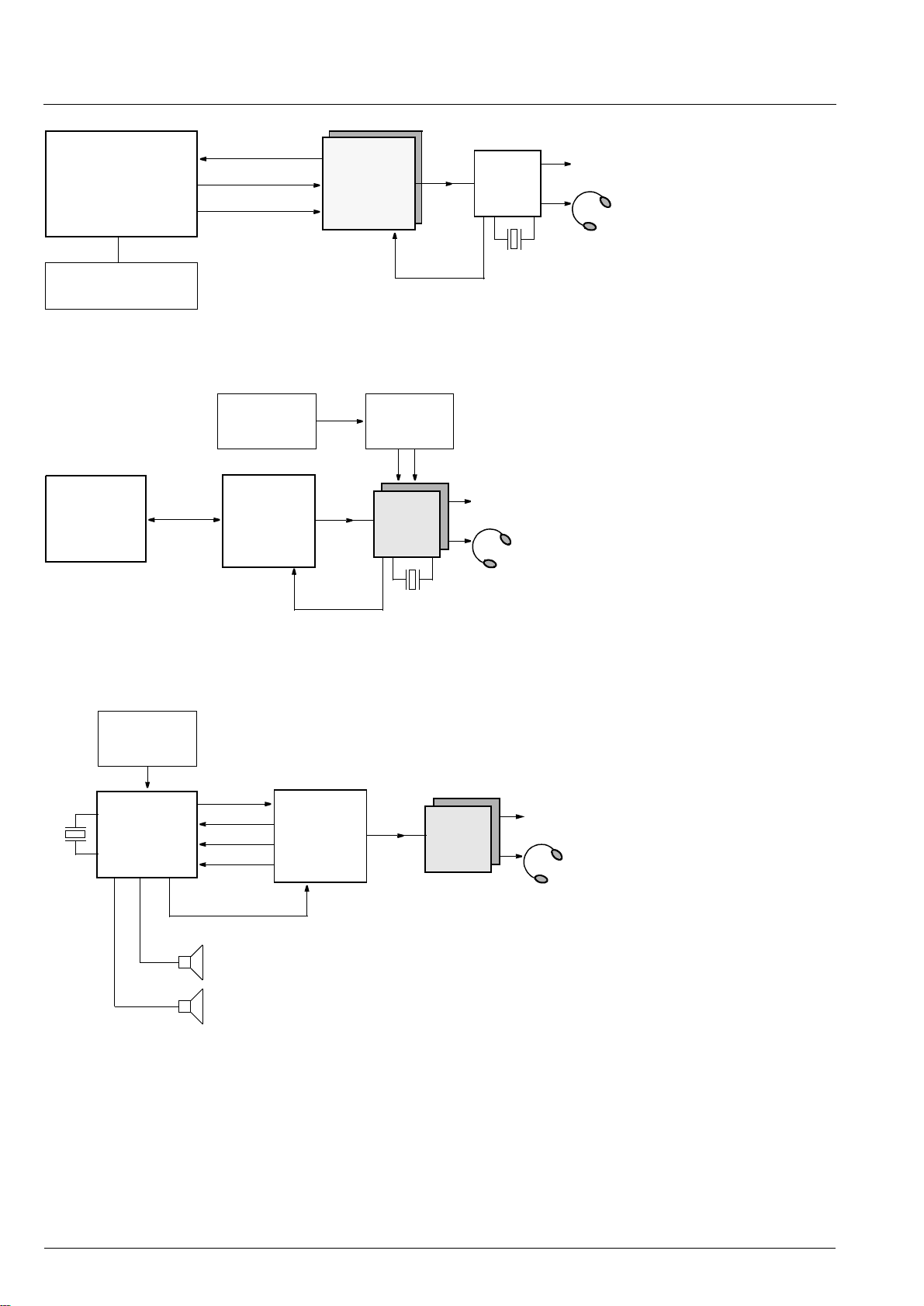
Fig. 4–10: MPEG Layer-3 Player
FM-TUNER DEMOD
Optical
DSP
Pickup
SERVO
line out
DAC
I2S
DAC
3550A
14.725 MHz
RL
line out
MAS
3507D
CLKOUT
I2S
&
DAC
3550A
3550A
Fig. 4–11: CD-Player with FM-Radio
TUNER
18.432 MHz
MSP
34xx
ADRBUS
DATA
BCLK
LRCLK
32 kHz
18.432 MHz
CLKOUT
DRP
3510 A
384 × fs
I2S
DAC
DAC
3550A
3550A
line-out
Fig. 4–12: ADR Receiver
30 Micronas
Page 31

DAC 3550A
Micronas 31
Page 32

DAC 3550A
5. Data Sheet History
1. Final data sh eet: “DAC 3550A Stereo Audio DAC,
Edition July 23, 1999, 6251-467-1DS. First release of
the final data sheet.
Micronas GmbH
Hans-Bunte-Strasse 19
D-79108 Freiburg (Germany)
P.O. Box 840
D-79008 Freiburg (Germany)
Tel. +49-761-517-0
Fax +49-761-517-2174
E-mail: [email protected]
Internet: www.micronas.com
Printed in Germany
Order No. 6251-467-1DS
All information and data contained in this data sheet are without any
commitment, are not to be considered as an offer for conclusion of a
contract, nor shall they be construed as to create any liability. Any new
issue of this data sheet invalidates previous issues. Product availability
and delivery are exclusively subject to our respective order confirmation
form; the same applies to orders based on development samples delivered. By this publication, Micronas GmbH does not assume responsibility for patent infr ingements or other right s of third parties whic h may
result from its use.
Further, Micronas GmbH reserves the right to revise this publication and
to make changes to its conte nt, at any t ime, withou t obligatio n to noti fy
any person or entity of such revisions or changes.
No part of this publication may be reproduced, photocopied, stored on a
retrieval system, or transmitted without the express written consent of
Micronas GmbH .
32 Micronas
Page 33

DAC 3550A
Preliminary Data Sheet Supplement
Subject:
Data Sheet Concerned:
New Package for DAC 3550A
DAC 3550A
6251-467-1PD, Edition April 23, 1999
Supplement:
Edition:
New Package for DAC 3550A: 49-Ball Plastic Ball Grid Array (PBGA49)
1. Outline Dimensions
No. 2/ 6251-467-1PD S
May 18, 1999
D0026/1E
Fig. 1:
49-Ball Plastic Ball Grid Array
(PBGA49)
Dimensions in mm
MICRONAS INTERMETALL page 1 of 3
Page 34

DAC 3550A PRELIMINARY DATA SHEET SUPPLEMENT
2. Pin Connections and Short Descriptions
NC = not connected, leave vacant
X = obligatory; connect a s descr ibed
in application circuit diagram
LV = if not used, leave vacant
VSS = if not used, connect to VSS
VDD= connect to VDD
Unassigned pins must be left vacant.
Pin No. / Pin ID Pin Name Type Connection
PMQFP
44-pin
PBGA
49-ball
(If not used)
Short Description
1 B5 AGNDC BID X Analog reference voltage
2 A6 AVSS1 SUPPLY X VSS 1 for audio back-end
3 B4 AVSS0 SUPPLY X VSS 0 for audio output amplifiers
4 NC LV Not connected
5 C4 OUTL OUT LV Audio output:
headphone left or speaker +
6 NC LV Not connected
7 A3 OUTR OUT LV Audio output:
headphone right or Speaker −
8 NC LV Not connected
9 A2 AVDD0 SUPPLY X VDD 0 for audio output amplifiers
10 A1 AVDD1 SUPPLY X VDD 1 for audio back-end
11 NC LV Not connected
12 C3 XTI IN X Quartz oscillator pin 1
13 C2 XTO BID X Quartz oscillator pin 2
14 D2 CLKOUT OUT LV Clock output
2
15 C1 SCL BID LV I
16 D3 SDA BID LV I
C clock
2
C data
17 D1 VSS SUPPLY X Digital VSS
18 E1 VDD SUPPLY X Digital VDD
2
19 F2 MCS1 IN X I
20 F1 MCS2 IN X I
C chip sSelect 1
2
C chip select 2
21 G1 DEECTRL IN VSS Deemphasis on/off control
22 NC LV Not connected
2
23 E3 CLI VSS I
24 F3 DAI IN VSS I
25 F4 WSI IN VSS I
S bit clock
2
S data
2
S frame identification
26 G4 PORQ IN VDD Power-on-reset, active-low
page 2 of 3 MICRONAS INTER METALL
Page 35
PRELIMINARY DATA SHEET SUPPLEMENT DAC 3550A
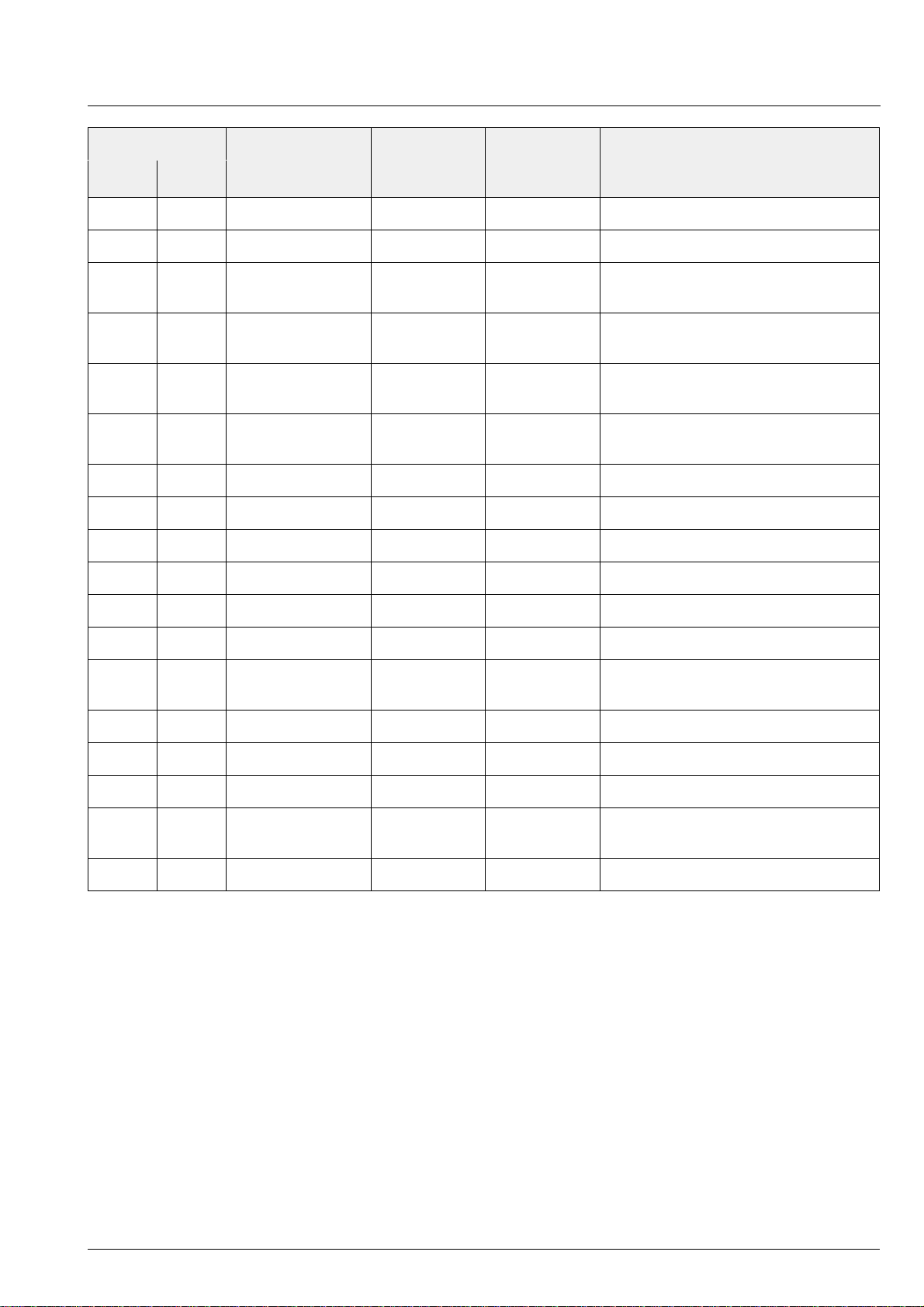
Pin No. / Pin ID Pin Name Type Connection
PMQFP
44-pin
PBGA
49-ball
(If not used)
Short Description
27 F5 TESTEN IN X Test enable
28 NC LV Not connected
29 G5 AUX2L IN LV AUX2 left input for external analog
signals (e.g. tape)
30 F6 AUX2R IN LV AUX2 right input for external analog
signals (e.g. tape)
31 G6 AUX1L IN LV AUX1 left input for external analog
signals (e.g. FM)
32 G7 AUX1R IN LV AUX1 right input for external analog
signals (e.g. FM)
33 NC LV Not connected
34 E5 DEEML OUT LV Deemphasis network, left
35 E6 DEEMR OUT LV Deemphasis network, right
36 NC LV Not connected
37 F7 FOUTL OUT X Output to left external filter
38 D6 FOPL BID X Filter op amp inverting input, left
39 E7 FINL IN/OUT X Input for FOUTL or
filter op amp output (line out)
40 NC LV Not connected
41 D7 FOUTR OUT X Output to right external filter
42 C6 FOPR BID X Right filter op amp inverting input
43 C7 FINR IN/OUT X Input for FOUTR or
filter op amp output (line out)
44 A7 VREF IN X Analog reference ground
MICRONAS INTERMETALL page 3 of 3
 Loading...