

Page 1
N
DAC14135
14-bit, 135MSPS D/A Converter
November 1999
DAC14135
14-bit, 135MSPS D/A Converter
General Description
The DAC14135 is a monolithic 14-bit, 135MSPS digital-to-analog
converter. The device has been optimized for use in cellular base
stations and other applications where high resolution, high
sampling rate, wide dynamic range, and compact size are
required. The DAC14135 has many integrated features including
a proprietary segmented DAC core, differential current outputs, a
band-gap voltage reference, and TTL/CMOS compatible inputs.
The converter features an 85dBc spurious free dynamic range
(SFDR) at low frequencies and a 70dBc SFDR with 20MHz
output signals. The 48-pin TSSOP package provides an extremely
small footprint for applications where space is a critical consideration. The DAC14135 operates from a single +5V power supply.
The digital power supply can also operate from +3.3V for lower
power consumption and compatibility with +3.3V data inputs. The
DAC14135 is fabricated in a 0.5µm CMOS process and is specified over the industrial temperature range of -40°C to +85°C.
National Semiconductor thoroughly tests each part to verify full
compliance with the guaranteed specifications.
Features
• 135 MSPS
• Wide dynamic range
SFDR @ 1MHz f
SFDR @ 5MHz f
SFDR @ 20MHz f
: 85dBc
out
: 79dBc
out
out
: 70dBc
• Differential Current Outputs
• Low power consumption: 185mW
• Very small package: 48-pin TSSOP
• TTL/CMOS (+3.3V or +5V) inputs
Applications
• Cellular Basestations:
GSM, WCDMA, DAMPS, etc.
• Multi-carrier Basestations
• Multi-standard Basestations
• Direct digital synthesis (DDS)
• ADSL modems
• HFC modems
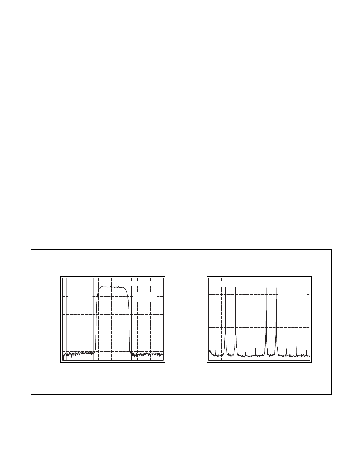
W-CDMA ACPR
-30
-40
-50
-60
-70
-80
Power (dB)
-90
-100
-110
-120
ACPR Lower
246810121416
72.1dB
Frequency (MHz)
Fs = 32.768MSPS
ACPR Upper
73dB
Four-Tone SFDR
0
SFDR > 70dBc
-20
-40
-60
Power (dB)
-80
-100
Fs = 135MSPS
F
= 6.2MHz
out1
F
= 9.31MHz
out2
= 18.8MHz
F
out3
F
= 21.95MHz
out4
Ampl. = 0dBFS
51015202530
Frequency (MHz)
© 1999 National Semiconductor Corporation http://www.national.com
Printed in the U.S.A.
Page 2
µ
µ
DAC14135
Electrical Characteristics
(sample rate = 135MSPS, T
full scale current = 20mA,
= -40°C, T
min
differential 50 Ω doubly terminated output, unless specified otherwise)
= +85°C, AV
max
= +5V, DV
DD
= +5V, CV
DD
= +5V,
DD
PARAMETERS CONDITIONS TEMP RATINGS UNITS NOTES
MIN TYP MAX
RESOLUTION
FULL SCALE CURRENT
MAXIMUM CONVERSION RATE
SFDR (1
SFDR (1
SFDR (1
ST
Nyquist band)
ST
Nyquist band)
ST
Nyquist band)
NOISE FLOOR
DYNAMIC LINEARITY @ DV
= +5V sample rate = 135MSPS
DD
spurious-free dynamic range 1
= 1MHz 0dBFS Full 75 85 dBc 2
f
out
f
= 5MHz 0dBFS Full 70 79 dBc 2
out
f
= 20MHz 0dBFS Full 64 70 dBc 1 , 2
out
SFDR within a band f
f
= 1MHz, 0dBFS Full 75 85 dBc 2
out
f
= 5MHz, 0dBFS Full 70 79 dBc 2
out
f
= 20MHz, 0dBFS Full 64 70 dBc 1 , 2
out
f
= 5MHz, 0dBFS +25°C -146 dBFS/Hz
out
ST
Nyquist band
= 20MHz, 4MHz band +25°C 90 dBc
out
Full 14 Bits 1
Full 20 mA
Full 135 150 MSPS 1 , 2
four-tone SFDR 6.2, 9.31, 18.8, 21.95 MHz +25°C 72 dBc
DYNAMIC LINEARITY @ DV
spurious-free dynamic range 1
= 1MHz 0dBFS, DV
f
out
f
= 5MHz 0dBFS, DV
out
f
= 20MHz 0dBFS, DV
out
= +3.3V sample rate = 100MSPS
DD
ST
Nyquist band
= +3.3V +25°C 83 dBc
DD
= +3.3V +25°C 77 dBc
DD
= +3.3V +25°C 70 dBc
DD
DYNAMIC CHARACTERISTICS
glitch impulse +25°C 1 pV-s 3
settling time to 0.1% step size = I
/2 +25°C 30 ns
fullscale
rise time +25°C 0.4 ns
fall time +25°C 0.4 ns
DC ACCURACY AND PERFORMANCE
differential non-linearity +25°C ±1.0 LSB
integral non-linearity +25°C ±1.5 LSB
gain error +25°C ±5.0 % of FS
gain drift 20mA output current Full ±75 ppm/°C
offset error +25°C 10 nA
reference voltage +25°C 1.111 1.235 1.358 V
ANALOG OUTPUT PERFORMANCE
full scale current +25°C 20 mA
compliance voltage (high) +25°C 1.25 V
compliance voltage (low) +25°C -0.5 V
output resistance at mid-scale +25°C 150 k Ω
output capacitance at mid-scale +25°C 8.5 pF
DATA INPUTS
input logic low voltage, V
input logic high voltage, V
input logic low voltage, V
input logic high voltage, V
input logic low current, I
input logic high current, I
IL
IH
IL
IH
IL
IH
DV
= +3.3V Full 0.9 V 1
DD
DV
= +3.3V Full 2.4 V 1
DD
Full 1.3 V 1
Full 3.5 V 1
Full -10 10
Full -10 10
A1
A1
TIMING
maximum conversion rate Full 135 150 MSPS 1, 2
setup time (T
hold time (T
propagation delay (T
latency +25°C 1
) +25°C 0.5 ns
S
) +25°C 4.5 ns
H
) +25°C 2 ns
PD
clk cycles
CLOCK INPUTS
clock inputs internal self bias +25°C 1.5 V
differential clock input swing Full 1.5 Vpp
differential clock input slew rate Full 1 V/ns
clock input impedance (single-ended) +25°C 1.2 k Ω
Min/max ratings are based on product characterization and simulation. Individual parameters are tested as noted. Outgoing quality levels are
determined from tested parameters.
http://www.national.com
2
Page 3
DAC14135
Electrical Characteristics
(sample rate = 135MSPS, T
full scale current = 20mA,
= -40°C, T
min
differential 50 Ω doubly terminated output, unless specified otherwise)
= +85°C, AV
max
= +5V, DV
DD
= +5V, CV
DD
= +5V,
DD
PARAMETERS CONDITIONS TEMP RATINGS UNITS NOTES
MIN TYP MAX
POWER REQUIREMENTS
analog supply current +25°C 28 35 mA 1
digital supply current 135MSPS, DV
digital supply current 100MSPS, DV
power consumption 135MSPS, DV
power consumption 100MSPS, DV
AV
power supply rejection ratio at mid-scale +25°C 1.0 %FS/V
DD
Min/max ratings are based on product characterization and simulation. Individual parameters are tested as noted. Outgoing quality levels are
determined from tested parameters.
1) These parameters are 100% tested at 25°C.
2) These parameters are sample tested at -40°C, +25°C and +85°C.
Absolute Maximum Ratings
positive supply voltage (V
analog output voltage range -0.7V to +V
digital input voltage range -0.5V to +V
output short circuit duration infinite
junction temperature 175°C
storage temperature range -65°C to 150°C
lead solder duration (+300°C) 10sec
Note: Absolute maximum ratings are limiting values , to be applied individually, and
beyond which the serviceability of the circuit may be impaired. Functional
operability under any of these conditions is not necessarily implied. Exposure to
maximum ratings for extended periods may affect device reliability.
) -0.5V to +6V
DD
= +5V +25°C 9 15 mA 1
DD
= +3.3V +25°C 4.5 mA
DD
= +5V +25°C 185 mW
DD
= +3.3V +25°C 150 mW
DD
CLC5958 Timing Diagram
Notes
3) Defined as the net area of undesired output transients in pV-s
at a major transition.
Recommended Operating Conditions
positive analog supply voltage +5V ±5%
positive digital supply voltage +3.3V or +5V ±5%
DD
positive clock supply voltage +5V ±5%
DD
operating temperature range -40°C to +85°C
Pac kage Thermal Resistance
Package
48-pin TSSOP 56°C/W 16°C/W
θ
JA
Pac kage Transistor Count
Transistor count 8,600
θ
JC
Ordering Information
Model Temperature Range Description
DAC14135MT -40°C to +85°C 48-pin TSSOP (industrial temperature range)
DAC14135MTX -40°C to +85°C 48-pin TSSOP (TNR 1000 pc reel)
DAC14135PCASM Fully loaded evaluation board with DAC14135 … ready for test.
D0 – D13
CLOCK T
IoutT or
IoutF
N-1
N N+1
T
S
T
H
T
PD
N-2
DA C14135 Timing Diagram
N
N-1
NOTE: 1 clock cycle latency
3
http://www.national.com
Page 4
DAC14135 Pin Definitions
(MSB)
(LSB)
1DGND 48 DGND
2DGND 47 DGND
3DGND 46 DGND
4DV
DD
5DV
DD
6 D13 43 CV
7D12 42 Clock T
DAC14135
8D11 41 Clock F
9D10 40 CGND
10D9 39 NC
11D8 38 AGND
12D7 37 I
13D6 36 I
14D5 35 AGND
15D4 34 AV
16D3 33 AV
17D2 32 AGND
18D1 31 REFCOMP
19D0 30 FSADJ
20DS 29 REFIO
21NC 28 REFLO
22AGND 27 AGND
23AGND 26 AGND
24AGND 25 AGND
45 DV
44 DV
OUTT
OUTF
DD
DD
DD
DD
DD
I
OUTT
I
OUTF
Clock T
(Pins 37, 36) Differential current outputs. Output compliance
range is -0.5V to +1.25V.
(Pins 42, 41) Differential clock inputs. Bypass CLOCKF with
Clock F a 0.1 µ F capacitor to CGND if using single-ended clock on
CLOCKT. Both inputs have internal self-bias at
approximately 1.5V.
D0 - D13 (Pins 6 - 19) Digital data inputs. CMOS (+3.3V and +5V) and
TTL (with +3.3V DVDD) compatible. D13 is the MSB.
DS (Pin 20) Data scramble input. If not used, either connect to
ground or leave unconnected.
AGND (Pins 22 - 27, 32, 35, 38) Analog ground.
DGND (Pins 1 - 3, 46 - 48) Digital ground.
CGND (Pin 40) Clock ground. Connect to AGND.
AV
DD
(Pins 33, 34) +5V power supply for the analog section.
Bypass to analog ground with a 0.1µF capacitor.
DV
DD
(Pins 4, 5, 44, 45) +5V or +3.3V power supply for the digital
section. Bypass to digital ground with a 0.1µF capacitor.
CV
DD
(Pin 43) Internal clock buffer power supply. Bypass to clock
ground with 0.1µF capacitor.
REFIO (Pin 29) Internal voltage reference output (Vref) or voltage
reference input. Nominally +1.235V. Can be overdriven with
an external reference. Bypass to A GND with 0.1µF capacitor.
REFLO (Pin 28) Ground for reference circuitry. Should be connected
to AGND.
FSADJ (Pin 30) Full scale current adjust. Must be connected with an
external resistor (Rset) or an external current source (Iref) to
analog ground.
Ifullscale (mA) = 42.67 x Iref = 42.67 x REFIO/Rset
REFCOMP (Pin 31) Compensation pin for the internal reference
circuitry. Bypass to analog ground with a 0.1µF capacitor.
NC (Pins 21, 39) No connect.
http://www.national.com
4
Page 5
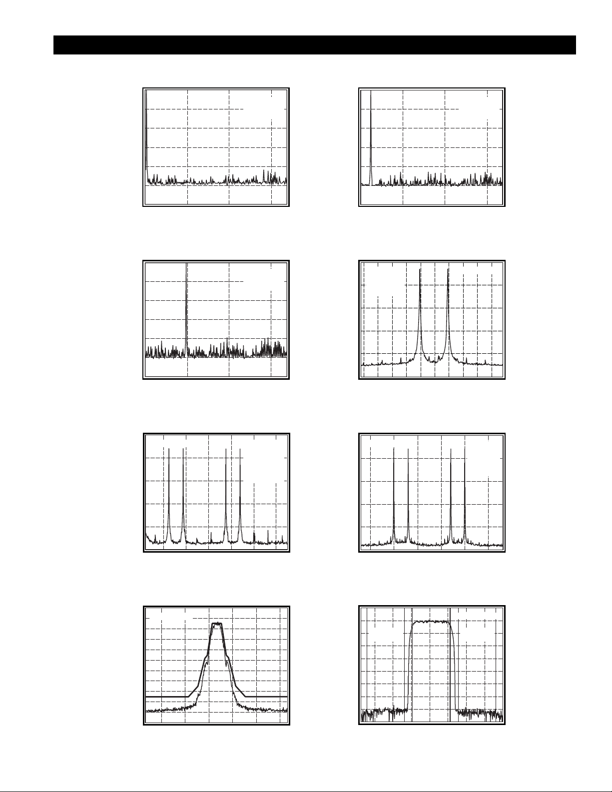
DAC14135 Typical Performance Characteristics
(AV
DD
= +5V, DVDD = +5V, CVDD = +5V, TA = 25°C)
Single-Tone SFDR
0
-20
-40
-60
Power (dB)
-80
-100
-120
0
Single-Tone SFDR
0
-20
-40
-60
Power (dB)
-80
-100
20
40
Frequency (MHz)
Fs = 135MSPS
= 1MHz
F
out
Ampl. = 0dBFS
60
Fs = 135MSPS
F
= 20MHz
out
Ampl. = 0dBFS
Single-Tone SFDR
0
-20
-40
-60
Power (dB)
-80
-100
-120
0
Two-Tone SFDR
0
Fs = 135MSPS
= 5MHz
F
out1
= 5.2MHz
F
-20
out2
Ampl. = 0dBFS
-40
-60
Power (dB)
-80
20
40
Frequency (MHz)
Fs = 135MSPS
= 5MHz
F
out
Ampl. = 0dBFS
60
SFDR > 77dBc
-120
0
Four-Tone SFDR
0
-20
-40
-60
Power (dB)
-80
-100
51015202530
GSM EDGE Modulation
0
Fs = 121.3MSPS
-10
-20
-30
-40
-50
-60
-70
Power (dB)
-80
-90
-100
-110
14 14.5 15 15.5 16 16.5
20
40
Frequency (MHz)
Frequency (MHz)
Frequency (MHz)
60
Fs = 135MSPS
F
= 6.2MHz
out1
= 9.31MHz
F
out2
= 18.8MHz
F
out3
= 21.95MHz
F
out4
Ampl. = 0dBFS
-100
4.6 4.7 4.8 4.9 5.0 5.1 5.2 5.3 5.4 5.5
Frequency (MHz)
Four-Tone SFDR
0
SFDR > 75dBcSFDR > 70dBc
-20
-40
-60
Power (dB)
-80
-100
91011121314
Frequency (MHz)
W-CDMA ACPR
-30
-40
ACPR Lower
-50
-60
70.5dB
-70
-80
Power (dB)
-90
-100
-110
-120
2 4 6 8 10 12 14 16
Frequency (MHz)
Fs = 135MSPS
F
= 10MHz
out1
= 10.6MHz
F
out2
F
= 12.4MHz
out3
F
= 13.0MHz
out4
Ampl. = 0dBFS
Fs = 65.536MSPS
ACPR Upper
71.5dB
5 http://www.national.com
Page 6

DAC14135 Typical Performance Characteristics
(AV
DD
= +5V, DVDD = +5V, CVDD = +5V, TA = 25°C)
dB
dB
90
85
80
75
70
65
60
100
90
80
70
60
SFDR vs. F
0
HD vs. F
0
10
, 0dBFS
out
65MSPS
100MSPS
10
out
20 30
F
(MHz)
out
@ 135MSPS, 0dBFS
20 30 40
F
(MHz)
out
135MSPS
HD4
HD3
HD2
SFDR vs. F
90
0dBFS
85
80
75
dB
70
65
60
40
0
HD vs. F
100
90
80
dB
70
60
50
0
@ 135MSPS
out
-6dBFS
-12dBFS
10
@ 100MSPS, DVDD = +3.3V
out
10
20 30
F
(MHz)
out
HD2
20 30 40
F
(MHz)
out
40
HD4
HD3
50
SNR vs. Fs @ 0dBFS 20mA, DC to F
80
75
70
dB
65
60
70
90 110
Fs(MSPS)
INL
2.0
1.0
0
LSB
-1.0
-2.0
0
5000
10000 15000
Code
130
/2
s
SFDR vs. Temp @ 135MSPS, 0dBFS
90
F
= 1MHz
out
85
80
dB
F
= 5MHz
out
75
F
= 20MHz
out
70
-45
050
85
Temperature (°C)
DNL
1.0
0.8
0.6
0.4
0.2
0
LSB
-0.2
-0.4
-0.6
-0.8
-1.0
0
5000
10000 15000
Code
http://www.national.com 6
Page 7

DAC14135 Application Information
Digital Data Inputs
The DAC14135’s 14-bit binary inputs are CMOS compatible.
The input voltage thresholds are approximately half of the
digital supply voltage (DVDD/2). For a 3.3V DVDD, the
inputs are also compatible with standard TTL levels.
Digital data is standard binary coded, D13 is the most
significant bit and D0 is the least significant bit. For all 1’s
at the input, I
input, I
OUTT
OUTT
= 0, I
= I
OUTF
fullscale
= I
fullscale
, I
= 0. For all 0’s at the
OUTF
.
To pre v ent or reduce digital data f eedthrough, k eep digital
data lines short and ensure separate digital grounding
(DGND). 75Ω resistors in series with the digital data input
path may be used to reduce overshoot and data
feedthrough to the analog outputs. Digital supply (DVDD)
should be decoupled to DGND using a 0.1µF bypass
capacitor.
Driving the Clock Inputs
The differential clock inputs, Clock T and Clock F, may be
driven by a variety of input sources. These pins are
internally self-biased at about 1.5V and therefore can be
differentially AC coupled. Alternatively, a single clock
source on Clock T with Clock F bypassed to CGND using
a 0.1µF capacitor, may be used to clock the DAC14135.
The clock driver supply voltage (CV
) should be 5V
DD
±5% and should be decoupled to the clock ground
(CGND) using a 0.1µF capacitor. For best SFDR
performance, use a differential clock input. Minimum
input voltage swing (1.5Vpp) and slew rate (1.0V/ns)
requirements should be met for optimum performance.
Low noise and low jitter clocks provide the best SNR
performance for the DAC14135. Figure 1 shows one
method of driving the clock inputs. A low noise sinusoidal
clock source (2-4 Vpp) may be used to drive the trans-
former primary.
The transformer converts the single ended clock signal to
a differential signal. The diodes in the secondary limit the
input swing to the DAC14135.
Latching the Input Data
Inputs of the DAC14135 include a master-slave flip-flop.
Due to internal clock buffer dela y, the DAC14135 requires
more hold time than setup time. This timing should be
observed at the DAC data and clock pins. Refer to the
timing diagram and the specifications for proper setup and
hold time requirements.
Data Scramble (DS) Input Pin
The DAC14135 is equipped with a data scramble input
pin (DS) that may be used to troubleshoot possible spurious or harmonic distortion degradation due to digital data
feedthrough on the printed circuit board. In the
DAC14135, the digital data inputs are logically XORed
with the DS input pin as shown in Figure 2.
DAC14135
D13
D12
•
•
•
•
•
D0
•
•
•
•
DQ
Q
DQ
Q
DQ
Q
CLK
DS
Figure 2: Digital Data Inputs with DS Input Pin
0.1µF
25Ω
25Ω
0.1µF
Clock T
0.1µF
Clock F
T1- 1T
Figure 1: Method of Driving Clock Inputs
If the DS pin is at logic low (DGND) the input data is left
unchanged and if this pin is at logic high (D V
) the input
DD
data is inverted. If the input data is XORed with a random
bit stream and if the same random bit stream is used to
drive the DS pin, low order harmonics due to data
feedthrough on the printed circuit board can be reduced.
If this feature is not used, tie DS pin to ground or leave it
floating (DS pin has internal active pulldown).
Voltage Reference Loop
The DAC14135 has an internal bandgap voltage
reference nominally at 1.235V. The output of this bandgap is connected to the REFIO pin. The REFIO pin is a
high impedance output and therefore can be easily over-
7 http://www.national.com
Page 8

ridden by an external bandgap reference voltage. The
reference ground (REFLO) should always be tied to
analog ground. The REFIO pin should be bypassed to
REFLO using a 0.1µF capacitor. For reduced noise, an
external compensation capacitor (0.1µF) should also be
used to bypass the internal reference loop from pin
REFCOMP to AGND. Figure 3 shows the internal
voltage reference loop functional schematic.
DAC14135
0.1µF
Band-
gap
1.235V
REFCOMP
REFIO
0.1µF
PMOS
mirrors
Analog Outputs
The differential analog outputs, I
OUTT
and I
OUTF
, are high
impedance current source outputs. These outputs, if
terminated into 50Ω at 20mA full scale current, will
generate a differential voltage output at 2Vpp. The output
compliance of each of the current outputs of the
DAC14135 is -0.5V to +1.25V. The differential outputs
can be converted to a single-ended output using an RF
center-tapped transformer or a differential to singleended amplifier. The I
OUTT
and I
traces on the
OUTF
printed circuit board should be short and matched with
adequate analog grounding nearby. One example of an
AC coupled differential to single-ended topology is shown
in Figure 4.
DAC14135
50
Ω
FSADJ
I
ref
Rset
REFLO
Figure 3: Internal Voltage Loop
Functional Schematic
A reference current source (Iref) from pin FSADJ to
ground may be used to set the full scale output current
(Ifs) of the DAC14135. The full scale current is given by,
Ifs = 42.67 x Iref
Alternatively, a resistor (Rset) from FSADJ to AGND may
be used to set the full scale output current of the DAC.
Ifs (mA) = 42.67 x REFIO/Rset
The voltage at REFIO is nominally set by the internal
bandgap at 1.235V. For a full scale output current of
20mA, the value of Rset is 2.635kΩ.
I
OUTT
T1-1T
I
OUTF
100
Ω
50
Ω
Figure 4: AC Coupled Differential to
Single-ended T opology
DAC14135 Grounding Information
In the DAC14135, all the grounds AGND, REFLO, DGND
and CGND are shorted together inside the package. The
purpose of having separate grounds on the printed circuit
board is to prevent digital data currents from returning
through the analog or reference grounds, and corrupting
the analog outputs. Refer to the evaluation board layout.
http://www.national.com 8
Page 9

DAC14135 Evaluation Board Description
General Description
The DAC14135 Evaluation Board is intended to aid in
evaluating the perfor mance of the DAC14135. The board
allows the user to exercise the inputs to the DAC and
examine the output in either differential or single ended
mode. The board comes complete with the DAC14135, a
transformer network to convert a single ended clock to a
differential clock, a transfor mer to convert the differential
output from I
OUTT
and I
to a single ended output,
OUTF
and an edge connector. This is a 5V part, but if a
3.3V CMOS or TTL digital data interface is required, the
digital supply (DVDD) should be 3.3V. A 3.3V regulator is
provided so that the board can be run off of a single
5V supply. For the best distortion performance at the
maximum clock frequency, D
should be set to 5V.
VDD
Setup and Configuration
There are two terminal blocks on the DAC14135
evaluation board, one in the upper left corner next to the
AMP connectors, and one in the upper right corner. The
upper right corner has the analog power supply
connector, marked +A
left is for the digital power supply and is marked +D
There is also a jumper next to the +D
marked D
with one end marked DIRECT and the
VDD
. The connector in the upper
VDD
terminal block
VDD
VDD
other end marked +3.3V REG.
There are three ways to power the evaluation board. The
default method of use is to connect the 5V power supply
to both the +A
terminal block and the +D
VDD
VDD
terminal
block and connect the jumper between the DIRECT pin
(pin 1) and the middle pin (pin 2).
If a 3.3V CMOS or TTL digital data interface is required,
connect the jumper between the +3.3V REG pin (pin 3)
and the middle pin (pin 2). This enables the 3.3V
regulator on the back side of the board. The output of the
regulator is filtered and powers the digital portion of
the DAC.
To use the board in the dual supply mode, connect a 5V
supply to the +A
supply to the +D
terminal block, connect a 3.3V
VDD
terminal block and connect the
VDD
jumper between the DIRECT pin (pin 1) and the middle
pin (pin 2). This bypasses the on-board voltage regulator,
although the regulator still draws power.
Getting Data to the Evaluation Board
The DAC14135 evaluation board is shipped with the
edge connectors J1 and J2 being the default data input
interface. J1 and J2 are AMP 536511-1 and 536511-3
edge connectors respectively. Data should be at the
same voltage level as D
. Figure 5 below, is an edge-
VDD
on view of J2. Pins 24D-11D are the data lines with 24D
being the MSB. The ground pins are 23C, 23A, 21C, 19C,
17C, 17A, 15C, 13C, 11C, 11A, 9C, 7C, 6A, 5C, 3C, and
1C. All ground pins are tied together on-board. Also, pin
10D should be at logic LOW (0V) if the data scramble
feature on the DAC14135 is not used.
Driving the Clock Input
The evaluation board has an on-board transformer, T2,
that converts a single ended clock to a differential
.
clock to drive the DAC14135. For best results drive the
CLOCK SMA connector with a low jitter 50Ω source. If a
sinusoidal source is used, its peak-to-peak amplitude
should be at least 2.5V to meet the minimum clock input
slew rate requirement. Back-to-back diodes at the secondary of the transformer T2 limit the voltage swing at
the DAC14135 Clock T and Clock F input pins.
Measuring the Analog Outputs
The evaluation board is shipped with transformer T1
installed to convert the differential output to a single
ended output. However, the 0Ω resistors R38 and R39
are not installed. To take single ended measurements,
install R38 and R39 and attach your instrument to the
SMA connector marked ‘SINGLE’. For differential output
measurements, remove R38 and R39 if they are
installed. Note that both outputs, I
OUTT
and I
terminated with 50Ω.
OUTF
, are
24D 23D 22D 21D 20D 19D 18D 17D 16D 15D 14D 13D 12D 11D 10D 9D 8D 7D 6D 5D 4D 3D 2D 1D
24C 23C 22C 21C 20C 19C 18C 17C 16C 15C 14C 13C 12C 11C 10C 9C 8C 7C 6C 5C 4C 3C 2C 1C
24B 23B 22B 21B 20B 19B 18B 17B 16B 15B 14B 13B 12B 11B 10B 9B 8B 7B 6B 5B 4B 3B 2B 1B
24A 23A 22A 21A 20A 19A 18A 17A 16A 15A 14A 13A 12A 11A 10A 9A 8A 7A 6A 5A 4A 3A 2A 1A
Figure 5: Pinout for J2 (Amp 536511-3)
9 http://www.national.com
Page 10
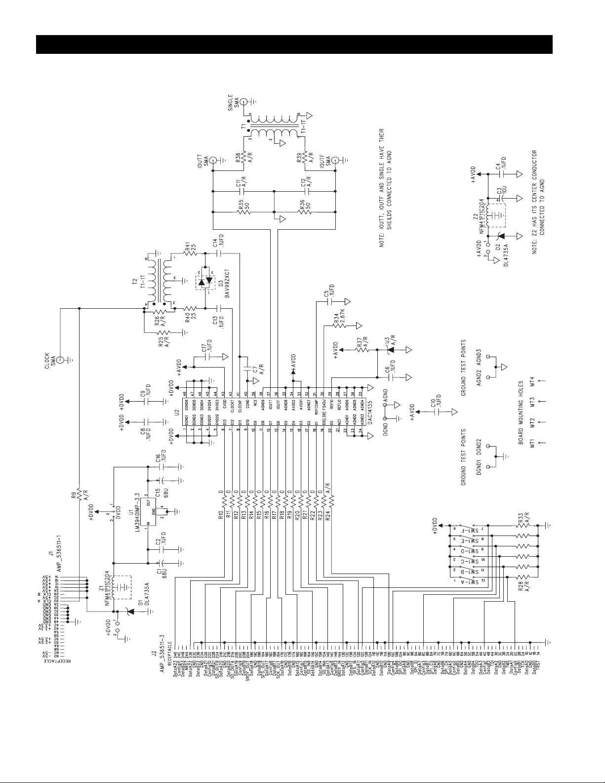
DAC14135 Evaluation Board Schematic
http://www.national.com 10
Page 11
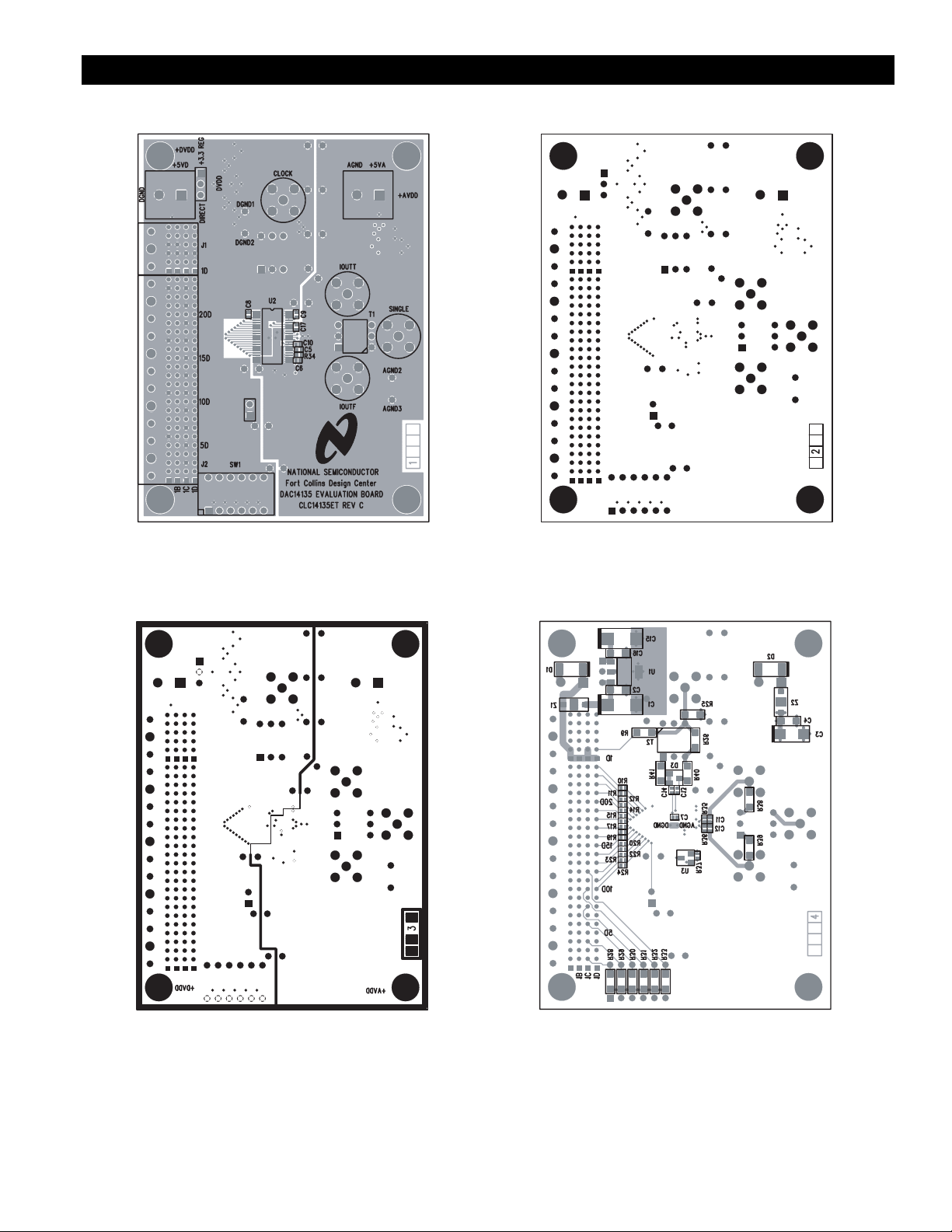
DAC14135 Evaluation Board Layout
DAC14135PCASM Layer 1 DAC14135PCASM Layer 2
DAC14135PCASM Layer 3 DAC14135PCASM Layer 4
11 http://www.national.com
Page 12

DAC14135
14-bit, 135MSPS D/A Converter
DAC14135 Physical Dimensions
Symbol Min Max Notes
A – 1.10
A1 0.05 0.15
A2 0.80 1.05
b 0.17 0.27
b1 0.17 0.23
c 0.09 0.20
c1 0.09 0.16
D 12.40 12.60 2
E 8.1 BSC
E1 6.00 6.20 2
e 0.50 BSC
L 0.50 0.75
L1 1.00 REF
R1 0.127
Notes:
1. All dimensions are in millimeters.
2. Dimensions D and E1 do not include mold protrusion.
Allowable protrusion is 0.20mm per side.
Customer Design Applications Support
National Semiconductor is committed to design excellence. For sales, literature and technical support, call the
National Semiconductor Customer Response Group at 1-800-272-9959 or fax 1-800-737-7018.
Life Support Policy
National’s products are not authorized for use as critical components in lif e support devices or systems without the e xpress written approv al
of the president of National Semiconductor Corporation. As used herein:
1. Life support devices or systems are devices or systems which, a) are intended for surgical implant into the body, or b) support or
sustain life, and whose failure to perform, when properly used in accordance with instructions for use provided in the labeling, can
be reasonably expected to result in a significant injury to the user.
2. A critical component is any component of a life support device or system whose failure to perform can be reasonably expected to
cause the failure of the life support device or system, or to affect its safety or effectiveness.
National Semiconductor National Semiconductor National Semiconductor National Semiconductor
Corporation Europe Hong Kong Ltd. Japan Ltd.
1111 West Bardin Road Fax: (+49) 0-180-530 85 86 2501 Miramar Tower Tel: 81-043-299-2309
N
National does not assume any responsibility for use of any circuitry described, no circuit patent licenses are implied and National reserves the right at any time without notice to change said
circuitry and specifications.
http://www.national.com 12
Arlington, TX 76017 E-mail: europe.support.nsc.com 1-23 Kimberley Road Fax: 81-043-299-2408
Tel: 1(800) 272-9959 Deutsch Tel: (+49) 0-180-530 85 85 Tsimshatsui, Kowloon
Fax: 1(800) 737-7018 English Tel: (+49) 0-180-532 78 32 Hong Kong
Francais Tel: (+49) 0-180-532 93 58 Tel: (852) 2737-1600
Italiano Tel: (+49) 0-180-534 16 80 Fax: (852) 2736-9960
 Loading...