

Datasheet DAC1232LIN, DAC1232LCWMX, DAC1232LCWM, DAC1232LCN, DAC1232LCJ Datasheet (NSC)
...Page 1
TL/H/5690
MICRO-DAC DAC1208/DAC1209/DAC1210/DAC1230/DAC1231/DAC1232
12-Bit, mP Compatible, Double-Buffered D to A Converters
February 1995
MICRO-DACTMDAC1208/DAC1209/DAC1210/DAC1230/
DAC1231/DAC1232 12-Bit, mP Compatible,
Double-Buffered D to A Converters
General Description
The DAC1208 and the DAC1230 series are 12-bit multiplying D to A converters designed to interface directly with a
wide variety of microprocessors (8080, 8048, 8085, Z-80,
etc.). Double buffering input registers and associated control lines allow these DACs to appear as a two-byte ‘‘stack’’
in the system’s memory or I/O space with no additional interfacing logic required.
The DAC1208 series provides all 12 input lines to allow single buffering for maximum throughput when used with 16-bit
processors. These input lines can also be externally configured to permit an 8-bit data interface. The DAC1230 series
can be used with an 8-bit data bus directly as it internally
formulates the 12-bit DAC data from its 8 input lines. All of
these DACs accept left-justified data from the processor.
The analog section is a precision silicon-chromium (Si-Cr)
R-2R ladder network and twelve CMOS current switches.
An inverted R-2R ladder structure is used with the binary
weighted currents switched between the I
OUT1
and I
OUT2
maintaining a constant current in each ladder leg independent of the switch state. Special circuitry provides TTL logic
input voltage level compatibility.
The DAC1208 series and DAC1230 series are the 12-bit
members of a family of microprocessor compatible DACs
(MICRO-DACs
TM
). For applications requiring other resolutions, the DAC1000 series for 10-bit and DAC0830 series
for 8-bit are available alternatives.
Features
Y
Linearity specified with zero and full-scale adjust only
Y
Direct interface to all popular microprocessors
Y
Double-buffered, single-buffered or flow through digital
data inputs
Y
Logic inputs which meet TTL voltage level specs (1.4V
logic threshold)
Y
Works withg10V referenceÐfull 4-quadrant
multiplication
Y
Operates stand-alone (without mP) if desired
Y
All parts guaranteed 12-bit monotonic
Y
DAC1230 series is pin compatible with the DAC0830
series 8-bit MICRO-DACs
Key Specifications
Y
Current Settling Time 1 ms
Y
Resolution 12 Bits
Y
Linearity (Guaranteed
over temperature) 10, 11, or 12 Bits of FS
Y
Gain Tempco 1.3 ppm/§C
Y
Low Power Dissipation 20 mW
Y
Single Power Supply 5 VDCto 15 V
DC
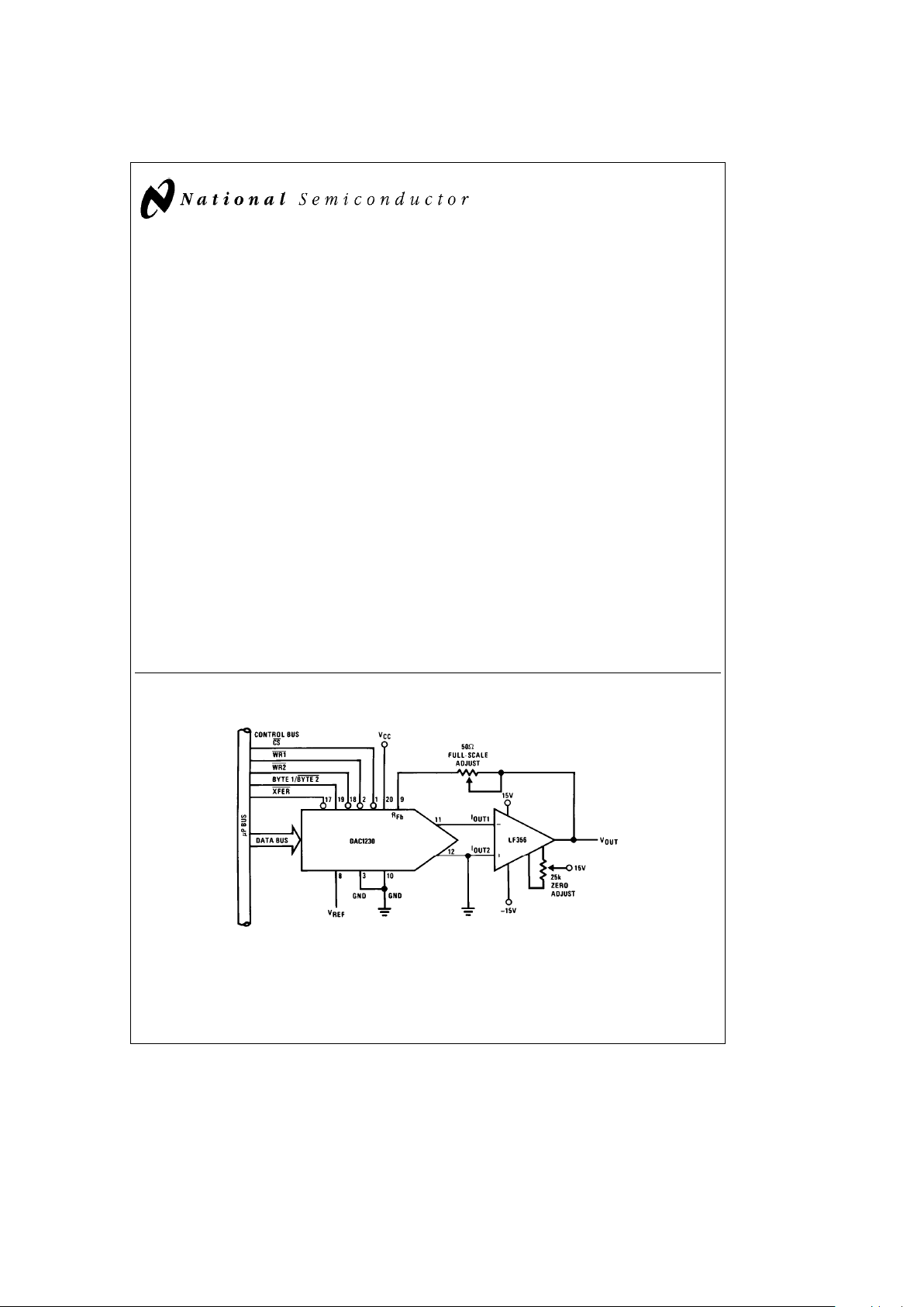
Typical Application
TL/H/5690– 1
TRI-STATEÉis a registered trademark of National Semiconductor Corp.
MICRO-DAC
TM
is a trademark of National Semiconductor Corp.
C
1995 National Semiconductor Corporation RRD-B30M115/Printed in U. S. A.
Page 2
Absolute Maximum Ratings
If Military/Aerospace specified devices are required,
please contact the National Semiconductor Sales
Office/Distributors for availability and specifications.
(Notes 1 and 2)
Supply Voltage (V
CC
)17V
DC
Voltage at Any Digital Input VCCto GND
Voltage at V
REF
Input
g
25V
Storage Temperature Range
b
65§Ctoa150§C
Package Dissipation at T
A
e
25§C 500 mW
(Note 3)
DC Voltage Applied to I
OUT1
or I
OUT2
(Note 4)
b
100 mV to V
CC
ESD Susceptability 800V
Operating Conditions
Lead Temperature (Soldering, 10 sec.) 300§C
Temperature Range T
MIN
s
T
A
s
T
MAX
DAC1208LCJ, DAC1209LCJ,
DAC1210LCJ, DAC1230LCJ,
DAC1231LCJ, DAC1232LCJ,
DAC1231LIN, DAC1232LIN
b
40§CsT
A
s
a
85§C
DAC1208LCJ-1, DAC1210LCJ-1,
DAC1230LCJ-1, DAC1231LCJ-1,
DAC1232LCJ-1, DAC1231LCN,
DAC1232LCN, DAC1231LCWM,
DAC1232LCWM 0
§
CsT
A
s
a
70§C
Range of V
CC
4.75 VDCto 16 V
DC
Voltage at Any Digital Input VCCto GND
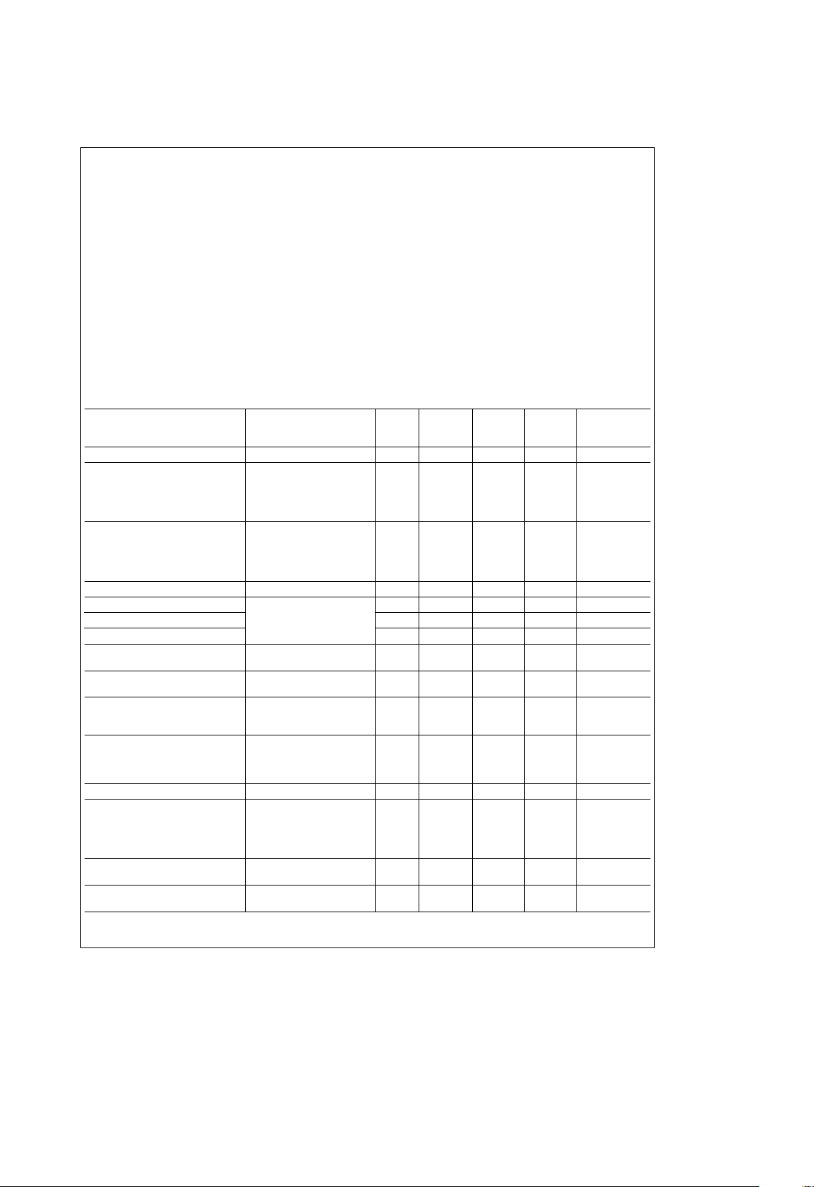
Electrical Characteristics
V
REF
e
10.000 VDC,V
CC
e
11.4 VDCto 15.75 VDCunless otherwise noted. Boldface limits apply from T
MIN
to T
MAX
(see
Note 13); all other limits T
A
e
T
J
e
25§C.
Typ
Tested Design
Parameter Conditions Notes
(Note 10)
Limit Limit Units
(Note 5) (Note 6)
Resolution 12 12 12 Bits
Linearity Error Zero and Full-Scale 4, 7, 13
(End Point Linearity) Adjusted
DAC1208, DAC1230
g
0.018g0.018 %ofFSR
DAC1209, DAC1231
g
0.024g0.024 %ofFSR
DAC1210, DAC1232
g
0.050g0.05 %ofFSR
Differential Non-Linearity Zero and Full-Scale 4, 7, 13
Adjusted
DAC1208, DAC1230
g
0.018g0.018 %ofFSR
DAC1209, DAC1231
g
0.024g0.024 %ofFSR
DAC1210, DAC1232
g
0.050g0.05 %ofFSR
Monotonicity 4 12 12 12 Bits
Gain Error (Min) Using Internal R
Fb
7
b
0.1 0.0 % of FSR
Gain Error (Max)
V
ref
e
g
10V,g1V
7
b
0.1
b
0.2 % of FSR
Gain Error Tempco 7
g
1.3
g
6.0 ppm of FS/§C
Power Supply Rejection All Digital Inputs
7
g
3.0
g
30 ppm of FSR/V
Latched High
Reference Input Resistance (Min)
13
15 10 10
kX
Reference Input Resistance (Max) 15 20 20
Output Feedthrough Error V
REF
e
20 Vp-p, fe100 kHz
All Data Inputs Latched 9 3.0 mVp-p
Low
Output Capacitance All Data Inputs I
OUT1
200 pF
Latched High I
OUT2
70 pF
All Data Inputs I
OUT1
70 pF
Latched Low I
OUT2
200 pF
Supply Current Drain 13 2.0 2.5 mA
Output Leakage Current
I
OUT1
All Data Inputs Latched 11, 13 0.1 15 15 nA
Low
I
OUT2
All Data Inputs Latched 11, 13 0.1 15 15 nA
High
Digital Input Threshold Low Threshold 13 0.8 0.8 V
DC
High Threshold 13 2.2 2.2 V
DC
Digital Input Currents Digital Inputsk0.8V 13
b
200
b
200 mA
DC
Digital Inputsl2.2V 13 10 10 mA
DC
2
Page 3
Electrical Characteristics (Continued)
V
REF
e
10.000 VDC,V
CC
e
11.4 VDCto 15.75 VDCunless otherwise noted. Boldface limits apply from T
MIN
to T
MAX
(see
Note 13); all other limits T
A
e
T
J
e
25§C.
See Typ
Tested Design
Symbol Parameter Conditions
Note (Note 10)
Limit Limit Units
(Note 5) (Note 6)
AC CHARACTERISTICS
t
s
Current Setting Time V
IL
e
0V, V
IH
e
5V 1.0 ms
t
W
Write and XFER V
IL
e
0V, V
IH
e
5V
8
50 320
Pulse Width Min. 320
t
DS
Data Setup Time Min. V
IL
e
0V, V
IH
e
5V 70 320
320
t
DH
Data Hold Time Min. V
IL
e
0V, V
IH
e
5V 30 90
ns
90
t
CS
Control Setup Time Min. V
IL
e
0V, V
IH
e
5V 60 320
320
t
CH
Control Hold Time Min. V
IL
e
0V, V
IH
e
5V 0 10
Note 1: Absolute Maximum Ratings indicate limits beyond which damage to the device may occur. DC and AC electrical specifications do not apply when operating
the device beyond its specified operating conditions.
Note 2: All voltages are measured with respect to GND, unless otherwise specified.
Note 3: This 500 mW specification applies for all packages. The low intrinsic power dissipation of this part (and the fact that there is no way to significantly modify
the power dissipation) removes concern for heat sinking.
Note 4: Both I
OUT1
and I
OUT2
must go to ground or the virtual ground of an operational amplifier. The linearity error is degraded by approximately V
OS
d
V
REF
. For
example, if V
REF
e
10Vthena1mVoffset, VOS,onI
OUT1
or I
OUT2
will introduce an additional 0.01% linearity error.
Note 5: Tested and guaranteed to National’s AOQL (Average Outgoing Quality Level).
Note 6: Design limits are guaranteed but not 100% tested. These limits are not used to calculate outgoing quality levels. Guaranteed for V
CC
e
11.4V to 15.75V
and V
REF
eb
10V toa10V.
Note 7: The unit FSR stands for full-scale range. Linearity Error and Power Supply Rejection specs are based on this unit to eliminate dependence on a particular
V
REF
value to indicate the true performance of the part. The Linearity Error specification of the DAC1208 is 0.012% of FSR(max). This guarantees that after
performing a zero and full-scale adjustment, the plot of the 4096 analog voltage outputs will each be within 0.012%
c
V
REF
of a straight line which passes through
zero and full-scale. The unit ppm of FSR(parts per million of full-scale range) and ppm of FS(parts per million of full-scale) are used for convenience to define specs
of very small percentage values, typical of higher accuracy converters. In this instance, 1 ppm of FSR
e
V
REF
/106is the conversion factor to provide an actual
output voltage quantity. For example, the gain error tempco spec of
g
6 ppm of FS/§C represents a worst-case full-scale gain error change with temperature from
b
40§Ctoa85§Cofg(6)(V
REF
/106)(125§C) org0.75 (10
b
3
)V
REF
which isg0.075% of V
REF
.
Note 8: This spec implies that all parts are guaranteed to operate with a write pulse or transfer pulse width (t
W
) of 320 ns. A typical part will operate with tWof only
100 ns. The entire write pulse must occur within the valid data interval for the specified t
W,tDS,tDH
and tSto apply.
Note 9: To achieve this low feedthrough in the D package, the user must ground the metal lid. If the lid is left floating the feedthrough is typically 6 mV.
Note 10: Typicals are at 25
§
C and represent the most likely parametric norm.
Note 11: A 10 nA leakage current with R
Fb
e
20k and V
REF
e
10V corresponds to a zero error of (10c10
b
9
c
20c103)c100% 10V or 0.002% of FS.
Note 12: Human body model, 100 pF discharged through a 1.5 kX resistor.
Note 13: Tested limit for
b
1 suffix parts applies only at 25§C.
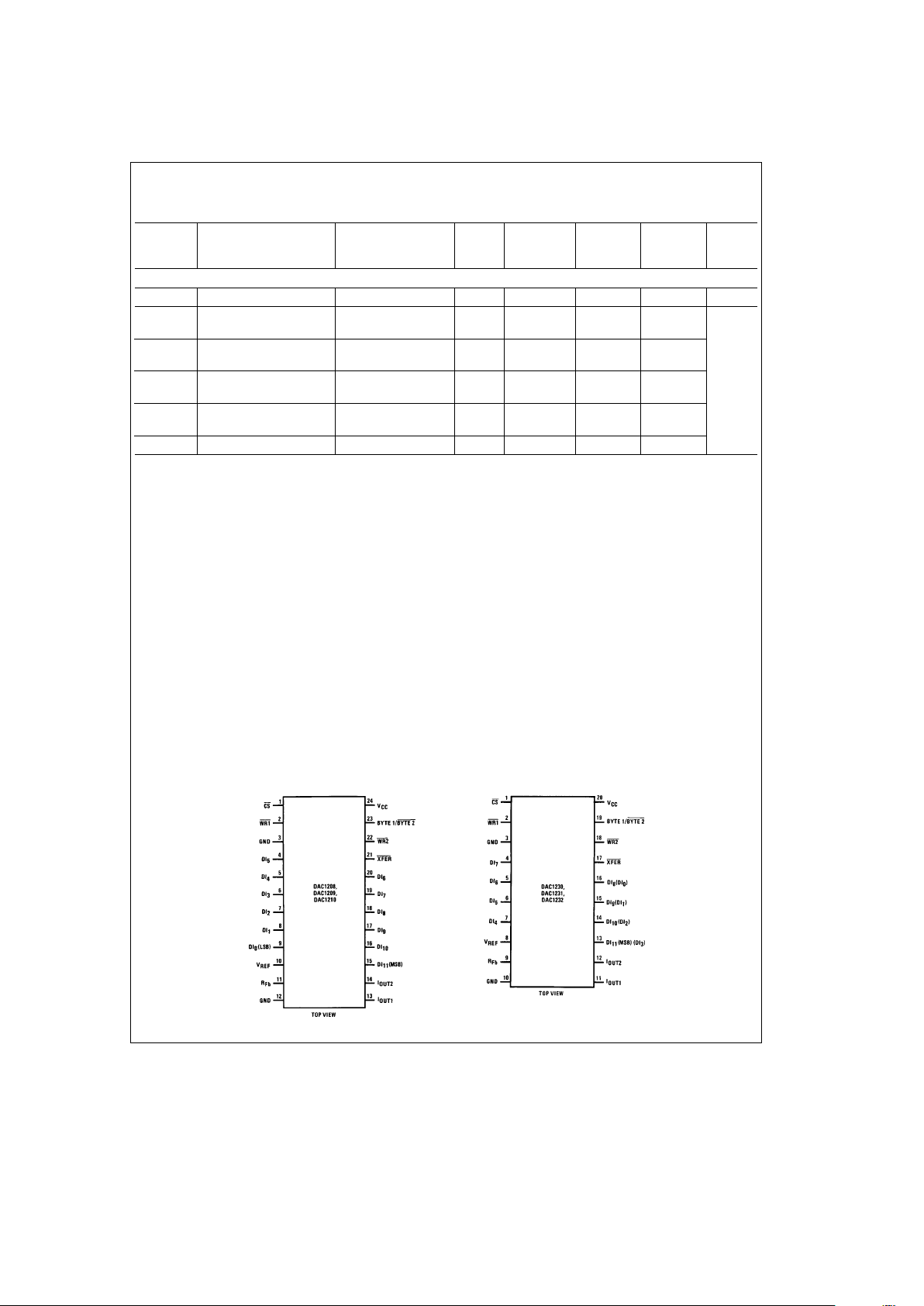
Connection Diagrams
Dual-In-Line Package Dual-In-Line Package
TL/H/5690– 2
See Ordering Information
3
Page 4
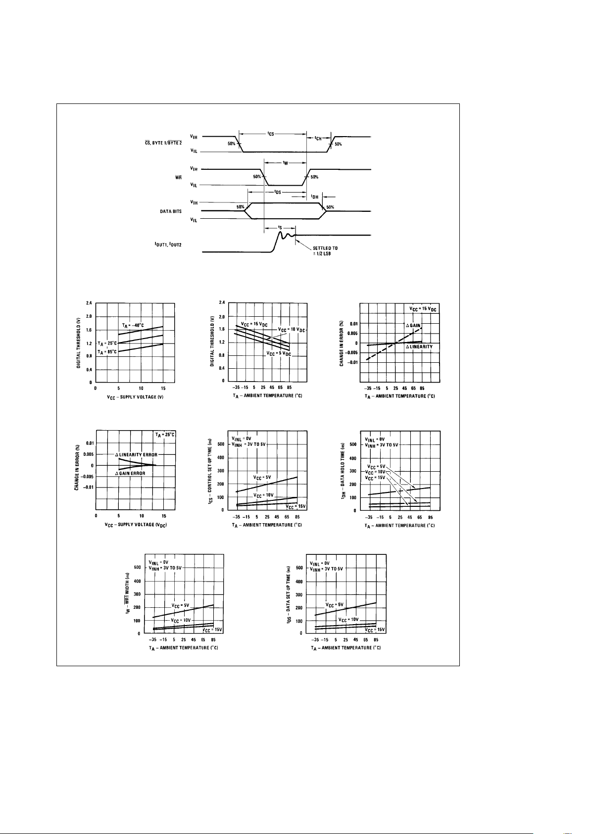
Switching Waveforms
TL/H/5690– 3
Typical Performance Characteristics
Digital Input Threshold
vs V
CC
Digital Input Threshold vs
Temperature
Gain and Linearity Error
Variation vs Temperature
Gain and Linearity Error
Variation vs Supply Voltage Control Set-Up Time, t
CS
Data Hold Time, t
DH
Write Pulse Width, t
W
Data Set-Up Time, t
DS
TL/H/5690– 4
4
Page 5
Definition of Package Pinouts
CONTROL SIGNALS (all control signals are level actuated)
CS: Chip Select (active low). The CS will enable WR1.
WR1: Write 1. The active low WR1 is used to load the digital
data bits (DI) into the input latch. The data in the input latch
is latched when WR1
is high. The 12-bit input latch is split
into two latches. One holds the first 8 bits, while the other
holds 4 bits. The Byte 1/Byte 2
control pin is used to select
both latches when Byte 1/Byte 2
is high or to overwrite the
4-bit input latch when in the low state.
Byte 1/Byte 2
: Byte Sequence Control. When this control is
high, all 12 locations of the input latch are enabled. When
low, only the four least significant locations of the input latch
are enabled.
WR2
: Write 2 (active low). The WR2 will enable XFER.
XFER: Transfer Control Signal (active low). This signal, in
combination with WR2
, causes the 12-bit data which is
available in the input latches to transfer to the DAC register.
DI
0
to DI11: Digital Inputs. DI0is the least significant digital
input (LSB) and DI
11
is the most significant digital input
(MSB).
I
OUT1
: DAC Current Output 1. I
OUT1
is a maximum for a
digital code of all 1s in the DAC register, and is zero for all
0s in the DAC register.
I
OUT2
: DAC Current Output 2. I
OUT2
is a constant minus
I
OUT1
,orI
OUT1
a
I
OUT2
e
constant (for a fixed reference
voltage). This constant current is
V
REF
c
#
1
b
1
4096
J
divided by the reference input resistance.
R
Fb
: Feedback Resistor. The feedback resistor is provided
on the IC chip for use as the shunt feedback resistor for the
external op amp which is used to provide an output voltage
for the DAC. This on-chip resistor should always be used
(not an external resistor) since it matches the resistors in
the on-chip R-2R ladder and tracks these resistors over
temperature.
V
REF
: Reference Voltage Input. This input connects an ex-
ternal precision voltage source to the internal R-2R ladder.
V
REF
can be selected over the range of 10V tob10V. This
is also the analog voltage input for a 4-quadrant multiplying
DAC application.
V
CC
: Digital Supply Voltage. This is the power supply pin for
the part. V
CC
can be from 5 VDCto 15 VDC. Operation is
optimum for 15 V
DC
.
GND: Pins 3 and 12 of the DAC1208, DAC1209, and
DAC1210 must be connected to ground. Pins 3 and 10 of
the DAC1230, DAC1231, and DAC1232 must be connected
to ground. It is important that I
OUT
1
and I
OUT
2
are at ground
potential for current switching applications. Any difference
of potential (V
OS
on these pins) will result in a linearity
change of
V
OS
3V
REF
For example, if V
REF
e
10V and these ground pins are 9
mV offset from I
OUT
1
and I
OUT
2
, the linearity change will be
0.03%.
Definition of Terms
Resolution: Resolution is defined as the reciprocal of the
number of discrete steps in the DAC output. It is directly
related to the number of switches or bits within the DAC. For
example, the DAC1208 has 2
12
or 4096 steps and therefore
has 12-bit resolution.
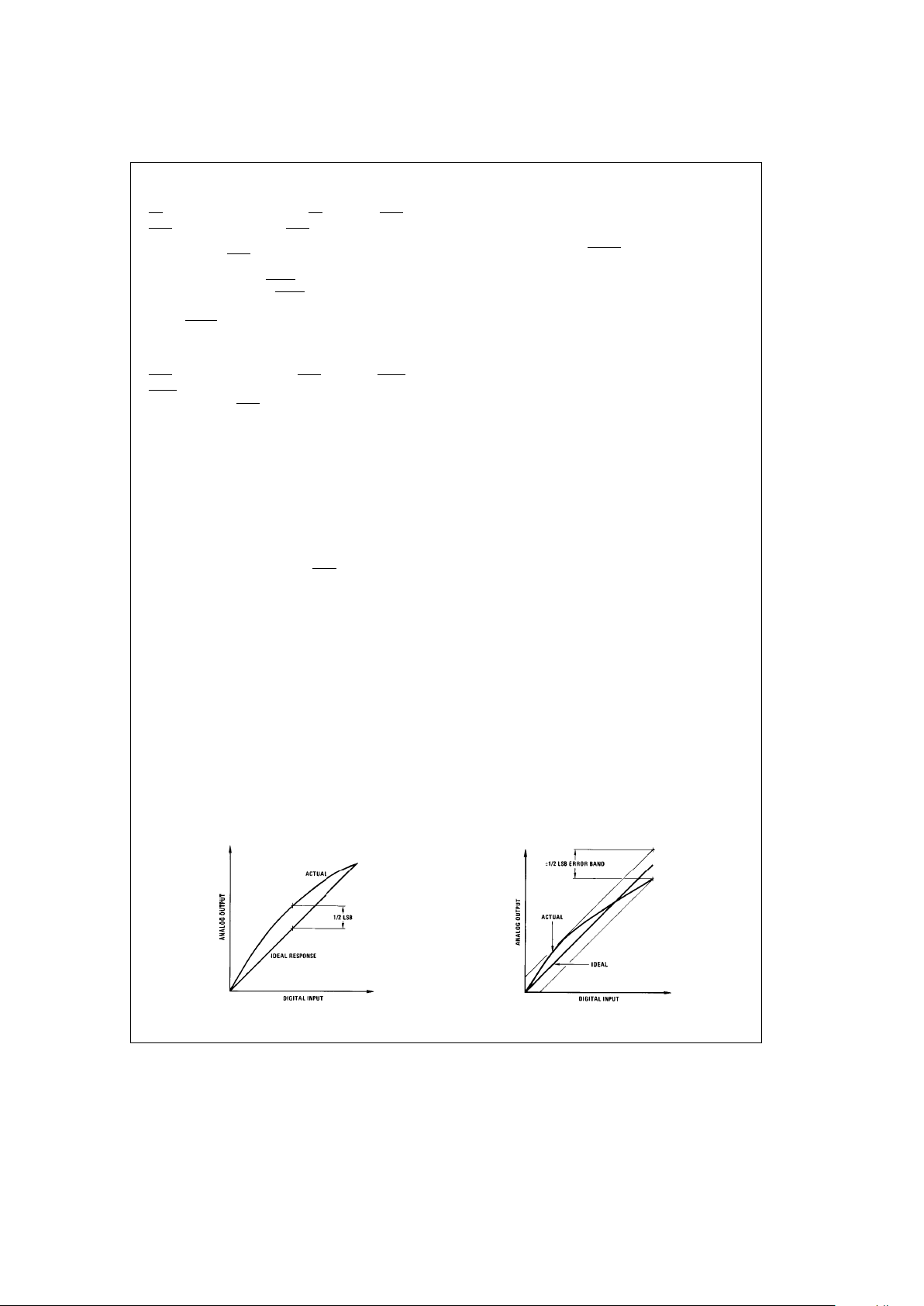
Linearity Error: Linearity error is the maximum deviation
from a
straight line passing through the endpoints of the
DAC transfer characteristic
. It is measured after adjusting
for zero and full-scale. Linearity error is a parameter intrinsic
to the device and cannot be externally adjusted.
National’s linearity test (a) and the best straight line test (b)
used by other suppliers are illustrated below. The best
straight line (b) requires a special zero and FS adjustment
for each part, which is almost impossible for the user to
determine. The end point test uses a standard zero FS adjustment procedure and is a much more stringent test for
DAC linearity.
Power Supply Sensitivity: Power supply sensitivity is a
measure of the effect of power supply changes on the DAC
full-scale output.
Settling Time: Full-scale current settling time requires zero
to full-scale or full-scale to zero output change. Settling time
is the time required from a code transition until the DAC
output reaches within
g
(/2 LSB of the final output value.
Full-Scale Error: Full-scale error is a measure of the output
error between an ideal DAC and the actual device output.
Ideally, for the DAC1208 or DAC1230 series, full-scale is
V
REF
b
1 LSB. For V
REF
e
10V and unipolar operation,
V
FULL-SCALE
e
10.0000Vb2.44 mVe9.9976V. Full-scale
error is adjustable to zero.
Differential Non-Linearity: The difference between any
two consecutive codes in the transfer curve from the theoretical 1 LSB is differential non-linearity.
Monotonic: If the output of a DAC increases for increasing
digital input code, then the DAC is monotonic. A 12-bit DAC
which is monotonic to 12 bits simply means that input increasing digital input codes will produce an increasing analog output.
TL/H/5690– 5
a) End Point Test After Zero
and FS Adjust
b) Shifting FS Adjust to Pass
Best Straight Line Test
5
Page 6
Application Hints
1.0 DIGITAL INTERFACE
These DACs are designed to provide all of the necessary
digital input circuitry to permit a direct interface to a wide
variety of microprocessor systems. The timing and logic level convention of the input control signals allow the DACs to
be treated as a typical memory device or I/O peripheral with
no external logic required in most systems. Essentially
these DACs can be mapped as a two-byte stack in memory
(or I/O space) to receive their 12 bits of input data in two
successive 8-bit data writing sequences. The DAC1230 series is intended for use in systems with an 8-bit data bus.
The DAC1208 series provides all 12 digital input lines which
can be externally configured to be controlled from an 8-bit
bus or can be driven directly from a 16-bit data bus.
All of the digital inputs to these DACs contain a unique
threshold regulator circuit to maintain TTL voltage level
compatibility independent of the applied V
CC
to the DAC.
Any input can also be driven from higher voltage CMOS
logic levels in non-microprocessor based systems. To prevent damage to the chip from static discharge, all unused
digital inputs should be tied to V
CC
or ground. As a troubleshooting aid, if any digital input is inadvertently left floating,
the DAC will interpret the pin as a logic ‘‘1’’.
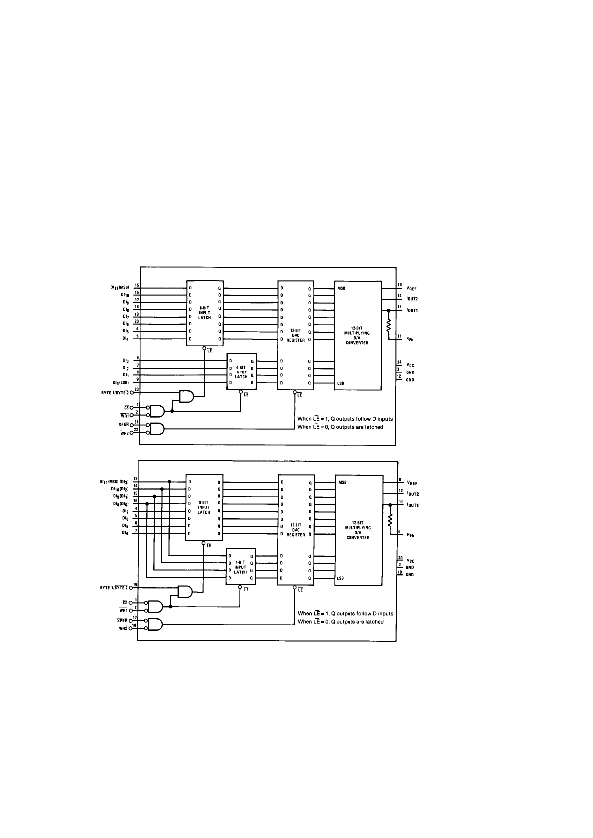
Double buffered digital inputs allow the DAC to internally
format the 12-bit word used to set the current switching R2R ladder network (see section 2.0) from two 8-bit data
write cycles.
Figures 1
and2show the internal data registers and their controlling logic circuitry. The timing diagrams
for updating the DAC output are shown in sections 1.1, 1.2
and 1.3 for three possible control modes. The method used
depends strictly upon the particular application.
FIGURE 1. DAC1208, DAC1209, DAC1210 Functional Diagram
TL/H/5690– 6
FIGURE 2. DAC1230, DAC1231, DAC1232 Functional Diagram
6
Page 7

Application Hints (Continued)
1.1 Automatic Transfer
The 12-bit DAC word is automatically transferred to the DAC register and the R-2R ladder when the second write (the 4 LSBs of
the data) occurs.
TL/H/5690– 7
1.2 Independent Processor Transfer Control
In this case a separate address is decoded to provide the XFER signal. This allows the processor to load the next required DAC
word but not change the analog output until some time later, most useful for the simultaneous updating of several DACs in a
system where their XFER
lines would be tied together.
TL/H/5690– 8
1.3 Transfer via an External Strobe
This method is basically the same as the previous operation except the XFER signal is provided by a device other than the
processor. This allows the DAC to hold the code for a conditional analog output signal which will be required on demand from an
external monitoring device (an analog voltage comparator for instance).
WR2 tied to a logic low (0V) TL/H/5690– 9
7
Page 8

Application Hints (Continued)
1.4 Left-Justified Data Format
It is important to realize that the input registers of these
DACs are arranged to accept a left-justified data word from
the microprocessor with the most significant 8 bits coming
first (Byte 1) and the lower 4 bits second. Left justification
simply means that the binary point is assumed to be located
to the left of the most significant bit.
Figure 3
shows how the
12 bits of DAC data should be arranged in 2 8-bit registers
of an 8-bit processor before being written to the DAC.
TL/H/5690-10
Xedon’t care
FIGURE 3. Left-Justified Data Format
1.5 16-Bit Data Bus Interface
The DAC1208 series provides all 12 digital input lines to
permit a direct parallel interface to a 16-bit data bus. In this
instance, double buffering is not always necessary (unless a
simultaneous updating of several DACs or a data transfer
via an external strobe is desired) so the 12-bit DAC register
can be wired to flow-through whereby its Q outputs always
reflect the state of its D inputs. The external connections
required and the timing diagram for this single buffered application are shown in
Figure 4
. Note that either left or rightjustified data from the processor can be accommodated
with a 16-bit data bus.
1.6 Flow-Through Operation
Through primarily designed to provide microprocessor interface compatibility, the MICRO-DACs can easily be configured to allow the analog output to continuously reflect the
state of an applied digital input. This is most useful in appli-
Interface Timing
TL/H/5690-11
XFER and WR2 grounded; Byte 1/Byte 2 tied to VCC.
FIGURE 4. 16-Bit Data Bus Interface for the DAC1208 Series
8
Page 9

Application Hints (Continued)
cations where the DAC is used in a continuous feedback
control loop and is driven by a binary up/down counter, or in
function generation circuits where a ROM is continuously
providing DAC data.
Only the DAC1208, DAC1209, DAC1210 devices can have
all 12 inputs flow-through. Simply grounding CS
, WR1, WR2
and XFER and tying Byte 1/Byte 2 high allows both internal
registers to follow the applied digital inputs (flow-through)
and directly affect the DAC analog output.
1.7 Address Decoding Tips
It is possible to map the MICRO-DACs into system ROM
space to allow more efficient use of existing address decoding hardware. The DAC in effect can share the same addresses of any number of ROM locations. The ROM outputs
will only be enabled by a READ of its address (gated by the
system READ strobe) and the DAC will only accept data
that is written to the same address (gated by the system
WRITE strobe).
The Byte 1/Byte 2
control function can easily be generated
by the processor’s least significant address bit (A0) by placing the DAC at two consecutive address locations and utilizing double-byte WRITE instructions which automatically increment or decrement the address. The CS
and XFER signals can then be decoded from the remaining address bits.
Care must be taken in selecting the actual address used
for Byte 1 of the DAC to prevent a carry (as a result of
incrementing the address for Byte 2) from propagating
through the address word and changing any of the bits decoded for CS
or XFER.
Figure 5
shows how to prevent this
effect.
The same problem can occur from a borrow when an autodecremented address is used; but only if the processor’s
address outputs are inverted before being decoded.
1.8 Control Signal Timing
When interfacing these MICRO-DACs to any microprocessor, there are two important time relationships that must be
considered to insure proper operation. The first is the minimum WR
strobe pulse width which is specified as 320 ns for
V
CC
e
11.4V to 15.75V and operation over temperature, but
typically a pulse width of only 250 ns is adequate. A second
consideration is that the guaranteed minimum data hold
time of 90 ns should be met or erroneous data can be
latched. This hold time is defined as the length of time data
must be held valid on the digital inputs
after
a qualified (via
CS
)WRstrobe makes a low to high transition to latch the
applied data.
If the controlling device or system does not inherently meet
these timing specs the DAC can be treated as a slow memory or peripheral and utilize a technique to extend the write
strobe. A simple extension of the write time, by adding a
wait state, can simultaneously hold the write strobe active
and data valid on the bus to satisfy the minimum WR
pulse
Write Address Bits
Cycle
15 2 1* 0**
First
01
(Byte 1) Decoded to
Second Address DAC 1 0
(Byte 2)
*Starting with a 0 prevents a carry on address incrementing.
**Used as Byte 1/Byte2
Control.
FIGURE 5
TL/H/5690-12
FIGURE 6. Accommodating a High Speed System
X ä Y
9
Page 10

Application Hints (Continued)
width. If this does not provide a sufficient data hold time at
the end of the write cycle, a negative edge triggered oneshot can be included between the system write strobe and
the WR
pin of the DAC. This is illustrated in
Figure 6
for an
exemplary system which provides a 250 ns WR
strobe time
with a data hold time of only 10 ns.
The proper data set-up time prior to the latching edge (low
to high transition) of the WR
strobe, is insured if the WR
pulse width is within spec and the data is valid on the bus for
the duration of the DAC WR
strobe.
1.9 Digital Signal Feedthrough
A typical microprocessor is a tremendous potential source
of high frequency noise which can be coupled to sensitive
analog circuitry. The fast edges of the data and address bus
signals generate frequency components of 10’s of megahertz and may cause fast transients to appear at the DAC
output, even when data is latched internally.
In low frequency or DC applications, low pass filtering can
reduce the magnitude of any fast transients. This is most
easily accomplished by over-compensating the DAC output
amplifier by increasing the value of its feedback capacitor.
In applications requiring a fast output response from the
DAC and op amp, filtering may not be feasible. In this event,
digital signals can be completely isolated from the DAC
circuitry, by the use of a DM74LS374 latch, until a valid
CS
signal is applied to update the DAC. This is shown in
Figure 7
.
A single TRI-STATEÉdata buffer such as the DM81LS95
can be used to isolate any number of DACs in a system.
Figure 8
shows this isolating circuitry and decoding hardware for a multiple DAC analog output card. Pull-up resistors are used on the buffer outputs to limit the impedance at
the DAC digital inputs when the card is not selected. A
unique feature of this card is that the DAC XFER
strobes are
controlled by the data bus. This allows a very flexible update
of any combination of analog outputs via a transfer word
which would contain a zero in the bit position assigned to
any of the DACs required to change to a new output value.
TL/H/5690-13
FIGURE 7. Isolating Data Bus from DAC Circuitry to Eliminate Digital Noise Coupling
10
Page 11

Application Hints (Continued)
TL/H/5690-14
FIGURE 8. TRI-STATEÉBuffers Isolate the Data and Control Lines from the DACs.
A Transfer Word Provides a Flexible Update.
11
Page 12

Application Hints (Continued)
2.0 ANALOG APPLICATIONS
The analog output signal for these DACs is derived from a
conventional R-2R current switching ladder network. A detailed description of this network can be found on the
DAC1000 series data sheet. Basically, output I
OUT1
provides a current directly proportional to the product of the
applied reference voltage and the digital input word. A second output, I
OUT2
will be a current proportional to the com-
plement of the digital input. Specifically:
I
OUT1
e
V
REF
R
c
D
4096
;
I
OUT2
e
V
REF
R
c
4095bD
4096
where D is the decimal equivalent of the applied 12-bit binary word (ranging from 0 to 4095), V
REF
is the voltage ap-
plied to the V
REF
terminal and R is the internal resistance of
the R-2R ladder. R is nominally 15 kX.
2.1 Obtaining a Unipolar Output Voltage
To maintain linearity of output current with changes in the
applied digital code, it is important that the voltages at both
of the current output pins be as near ground potential (0
V
DC
) as possible. With V
REF
ea
10V every millivolt appear-
ing at either I
OUT1
or I
OUT2
will cause a 0.01% linearity
error. In most applications this output current is converted to
a voltage by using an op amp as shown in
Figure 9
.
The inverting input of the op amp is a virtual ground created
by the feedback from its output through the internal 15 kX
resistor, R
Fb
. All of the output current (determined by the
digital input and the reference voltage) will flow through R
Fb
to the output of the amplifier. Two-quadrant operation can
be obtained by reversing the polarity of V
REF
thus causing
I
OUT1
to flow into the DAC and be sourced from the output
of the amplifier. The output voltage, in either case, is always
equal to I
OUT1
c
RFband is the opposite polarity of the ref-
erence voltage.
The reference can be either a stable DC voltage source or
an AC signal anywhere in the range from
b
10V toa10V.
The DAC can be thought of as a digitally controlled attenuator: the output voltage is always less than the applied reference voltage. The V
REF
terminal of the device presents a
nominal impedance of 15 kX to ground to external circuitry.
Always use the internal R
Fb
resistor to create an output
voltage since this resistor matches (and tracks with temperature) the value of the resistors used to generate the output
current (I
OUT1
).
The selected op amp should have as low a value of input
bias current as possible. The product of the bias current
times the feedback resistance creates an output voltage error which can be significant in low reference voltage applications. BI-FET
TM
op amps are highly recommended for use
with these DACs because of their very low input current.
TL/H/5690– 15
V
OUT
eb
(I
OUT1
c
RFb)
e
b
V
REF
(D)
4096
for 0
sDs
4095
FIGURE 9. Unipolar Output Configuration
BI-FETTMis a trademark of National Semiconductor Corp.
12
Page 13

Application Hints (Continued)
Transient response and settling time of the op amp are important in fast data throughput applications. The largest stability problem is the feedback pole created by the feedback
resistance, R
Fb
, and the output capacitance of the DAC.
This appears from the op amp output to the (
b
) input and
includes the stray capacitance at this node. Addition of a
lead capacitance, C
C
in
Figure 9
, greatly reduces overshoot
and ringing at the output for a step change in DAC output
current.
2.1.1 Zero and Full-Scale Adjustments
For accurate conversions, the input offset voltage of the
output amplifier must always be nulled. Amplifier offset errors create an overall degradation of DAC linearity.
The fundamental purpose of zeroing is to make the voltage
appearing at the DAC outputs as near 0 V
DC
as possible.
This is accomplished by shorting out R
Fb
, the amplifier feed-
back resistor, and adjusting the v
OS
nulling potentiometer of
the op amp until the output reads zero volts. This is done, of
course, with an applied digital code of all zeros if I
OUT1
is
driving the op amp (all ones for I
OUT2
). The short around
R
Fb
is then removed and the converter is zero adjusted.
A unique feature of this series of DACs is that the full-scale
or gain error is guaranteed to be negative. The gain error
specification is a measure of how close the value of the
internal feedback resistor, R
Fb
, matches the R-2R ladder
resistors. A negative gain error indicates that R
Fb
is a smaller resistance value than it should be. To adjust this gain
error, some resistance must always be added in series with
R
Fb
. The 50X potentiometer shown is sufficient to adjust
the worst-case gain error for these devices.
2.2 Bipolar Output Voltage from a Fixed Reference
The addition of a second op amp to the unipolar circuit can
generate a bipolar output voltage from a fixed reference
voltage. This, in effect, gives sign significance to the MSB of
the digital input word to allow two quadrant multiplication of
the reference voltage. The polarity of the reference can also
be reversed to realize full 4-quadrant multiplication. This circuit is shown in
Figure 10
.
This configuration features several improvements over existing circuits for a bipolar output shown with other multiplying DACs. Only the offset voltage of amplifier 1 affects the
linearity of the DAC. The offset voltage error of the second
op amp (although a constant output error) has no effect on
linearity. In addition, this configuration offers a non-interactive positive and negative full-scale calibration procedure.
TL/H/5690-16
V
OUT
e
V
REF
#
Db2048
2048
J
for 0sDs4095
1 LSB
e
l
V
REF
l
2048
Input Code Ideal V
OUT
MSB......LSB
a
V
REF
b
V
REF
111111111111 V
REF
b
1 LSB
b
l
V
REF
l
a
1 LSB
110000000000 V
REF
/2
b
l
V
REF
l
/2
100000000000 0 0
011111111111
b
1 LSB
a
1 LSB
001111111111
b
V
REF
2
b
1 LSB
l
V
REF
l
2
a
1 LSB
000000000000
b
V
REF
a
l
V
REF
l
FIGURE 10. Bipolar Output Voltage Configuration
13
Page 14

Application Hints (Continued)
2.2.1 Zero and Full-Scale Adjustments
To calibrate the bipolar output circuit, three adjustments are
required. The first step is to set all of the digital inputs LOW
(to force I
OUT1
to 0) then null the VOSof amplifier 1 by
setting the voltage at its inverting input (pin 2) to zero volts.
Next, with a code of all zeros still applied, adjust ‘‘
b
full-
scale adjust’’, the reference voltage, for V
OUT
e
g
l
V
REF
id-
eal
l
. The polarity of the output voltage at this time will be
opposite that of the applied reference. Finally, set all of the
digital inputs HIGH and adjust ‘‘
a
full-scale adjust’’ for
V
OUT
e
V
REF
2047
2048
.
The polarity of the output will be the same as that of the
reference voltage.
3.0 APPLICATION IDEAS
In this section the digital input word is represented by the
letter D and is equal to the decimal equivalent of the 12-bit
binary input. Hence D can be any integer value between 0
and 4095.
Composite Amplifier for Good DC Characteristics and Fast Output Response
#
Combines the low VOS,
low V
OS
drift and low
bias current of the
LM11 with the fast
response of the LF351.
#
Settling time&8 mS
for a zero to full-
scale transition
High Voltage, Power DAC
V
OUT
e
b
V
REF
D
4096
Ð
1
a
R2
R
Fb
a
R2
R1
(
TL/H/5690– 17
14
Page 15

Application Hints (Continued)
High Current Controller
I
O
e
1 Amp(D)
4096
TL/H/5690– 18
8-Bit Course, 4-Bit Vernier DAC
TL/H/5690– 20
15
Page 16

Ordering Information
Part Number Non-Linearity Package
Temperature
Range
DAC1208LCJ 0.018% J24A Cerdip
b
40§Ctoa85§C
DAC1208LCJ-1 0.018% J24A Cerdip 0§Ctoa70§C
DAC1209LCJ 0.024% J24A Cerdip
b
40§Ctoa85§C
DAC1210LCJ 0.050% J24A Cerdip
b
40§Ctoa85§C
DAC1210LCJ-1 0.050% J24A Cerdip 0§Ctoa70§C
DAC1230LCJ 0.018% J20A Cerdip
b
40§Ctoa85§C
DAC1230LCJ-1 0.018% J20A Cerdip 0§Ctoa70§C
DAC1231LCJ 0.024% J20A Cerdip
b
40§Ctoa85§C
DAC1231LCJ-1 0.024% J20A Cerdip 0§Ctoa70§C
DAC1231LCN 0.024% N20A Plastic 0§Ctoa70§C
DAC1231LCWM 0.024% M20B SO 0§Ctoa70§C
DAC1231LIN 0.024% N20A Plastic
b
40§Ctoa85§C
DAC1232LCJ 0.050% J20A Cerdip
b
40§Ctoa85§C
DAC1232LCJ-1 0.050% J20A Cerdip 0§Ctoa70§C
DAC1232LCN 0.050% N20A Plastic 0§Ctoa70§C
DAC1232LCWM 0.050% M20B SO 0§Ctoa70§C
DAC1232LIN 0.050% N20A Plastic
b
40§Ctoa85§C
16
Page 17

Physical Dimensions inches (millimeters)
20-Lead Ceramic Dual-In-Line Package (J)
Order Number DAC1230LCJ, DAC1230LCJ-1,
DAC1231LCJ, DAC1231LCJ-1, DAC1232LCJ or DAC1232LCJ-1
NS Package Number J20A
24-Lead Ceramic Dual-In-Line Package (J)
Order Number DAC1208LCJ, DAC1208LCJ-1,
DAC1209LCJ, DAC1210LCJ or DAC1210LCJ-1
NS Package Number J24A
17
Page 18

MICRO-DAC DAC1208/DAC1209/DAC1210/DAC1230/DAC1231/DAC1232
12-Bit, mP Compatible, Double-Buffered D to A Converters
Physical Dimensions inches (millimeters) (Continued)
20-Lead Molded Small Outline Package (M)
Order Number DAC1231LCWM or DAC1232LCWM
NS Package Number M20B
20-Lead Molded Dual-In-Line Package (N)
Order Number DAC1231LCN, DAC1231LIN, DAC1232LCN or DAC1232LIN
NS Package Number N20A
LIFE SUPPORT POLICY
NATIONAL’S PRODUCTS ARE NOT AUTHORIZED FOR USE AS CRITICAL COMPONENTS IN LIFE SUPPORT
DEVICES OR SYSTEMS WITHOUT THE EXPRESS WRITTEN APPROVAL OF THE PRESIDENT OF NATIONAL
SEMICONDUCTOR CORPORATION. As used herein:
1. Life support devices or systems are devices or 2. A critical component is any component of a life
systems which, (a) are intended for surgical implant support device or system whose failure to perform can
into the body, or (b) support or sustain life, and whose be reasonably expected to cause the failure of the life
failure to perform, when properly used in accordance support device or system, or to affect its safety or
with instructions for use provided in the labeling, can effectiveness.
be reasonably expected to result in a significant injury
to the user.
National Semiconductor National Semiconductor National Semiconductor National Semiconductor
Corporation Europe Hong Kong Ltd. Japan Ltd.
1111 West Bardin Road Fax: (
a
49) 0-180-530 85 86 13th Floor, Straight Block, Tel: 81-043-299-2309
Arlington, TX 76017 Email: cnjwge@tevm2.nsc.com Ocean Centre, 5 Canton Rd. Fax: 81-043-299-2408
Tel: 1(800) 272-9959 Deutsch Tel: (
a
49) 0-180-530 85 85 Tsimshatsui, Kowloon
Fax: 1(800) 737-7018 English Tel: (
a
49) 0-180-532 78 32 Hong Kong
Fran3ais Tel: (
a
49) 0-180-532 93 58 Tel: (852) 2737-1600
Italiano Tel: (
a
49) 0-180-534 16 80 Fax: (852) 2736-9960
National does not assume any responsibility for use of any circuitry described, no circuit patent licenses are implied and National reserves the right at any time without notice to change said circuitry and specifications.
 Loading...