

Page 1
1
Motorola Bipolar Power Transistor Device Data
These complementary silicon power transistors are designed for high–speed
switching applications, such as switching regulators and high frequency inverters.
The devices are also well–suited for drivers for high power switching circuits.
• Fast Switching — tf = 90 ns (Max)
• Key Parameters Specified @ 100_C
• Low Collector–Emitter Saturation Voltage —
V
CE(sat)
= 1.0 V (Max) @ 8.0 A
• Complementary Pairs Simplify Circuit Designs
MAXIMUM RATINGS
Rating
Symbol
ОООООООО
ОООООООО
ОООООООО
Value
ÎÎÎÎ
ÎÎÎÎ
ÎÎÎÎ
Unit
Collector–Emitter Voltage
V
CEO
ОООООООО
ОООООООО
ОООООООО
80
ÎÎÎÎ
ÎÎÎÎ
ÎÎÎÎ
Vdc
Collector–Emitter Voltage
V
CEV
ОООООООО
ОООООООО
ОООООООО
100
ÎÎÎÎ
ÎÎÎÎ
ÎÎÎÎ
Vdc
Emitter Base Voltage
V
EB
ОООООООО
ОООООООО
ОООООООО
7.0
ÎÎÎÎ
ÎÎÎÎ
ÎÎÎÎ
Vdc
Collector Current — Continuous
— Peak (1)
I
C
I
CM
ОООООООО
ОООООООО
ОООООООО
15
20
ÎÎÎÎ
ÎÎÎÎ
ÎÎÎÎ
Adc
Total Power Dissipation @ TC = 25_C
Derate above 25_C
P
D
ОООООООО
ОООООООО
ОООООООО
ОООООООО
83
0.67
ÎÎÎÎ
ÎÎÎÎ
ÎÎÎÎ
ÎÎÎÎ
Watts
W/_C
Operating and Storage Junction Temperature Range
TJ, T
stg
ОООООООО
ОООООООО
ОООООООО
–55 to 150
ÎÎÎÎ
ÎÎÎÎ
ÎÎÎÎ
_
C
THERMAL CHARACTERISTICS
Characteristic
Symbol
ОООООООО
ОООООООО
ОООООООО
Max
ÎÎÎÎ
ÎÎÎÎ
ÎÎÎÎ
Unit
Thermal Resistance, Junction to Case
R
θJC
ОООООООО
ОООООООО
ОООООООО
1.5
ÎÎÎÎ
ÎÎÎÎ
ÎÎÎÎ
_
C/W
Thermal Resistance, Junction to Ambient
R
θJA
ОООООООО
ОООООООО
ОООООООО
62.5
ÎÎÎÎ
ÎÎÎÎ
ÎÎÎÎ
_
C/W
Maximum Lead Temperature for Soldering
Purposes: 1/8″ from Case for 5 Seconds
T
L
ОООООООО
ОООООООО
ОООООООО
ОООООООО
275
ÎÎÎÎ
ÎÎÎÎ
ÎÎÎÎ
ÎÎÎÎ
_
C
(1) Pulse Width v 6.0 ms, Duty Cycle v 50%.
NOTE: All polarities are shown for NPN transistors. For PNP transistors, reverse polarities.
SEMICONDUCTOR TECHNICAL DATA
Order this document
by D44VH/D
Motorola, Inc. 1995
15 AMPERE
COMPLEMENTARY
SILICON
POWER TRANSISTORS
80 VOLTS
83 WATTS
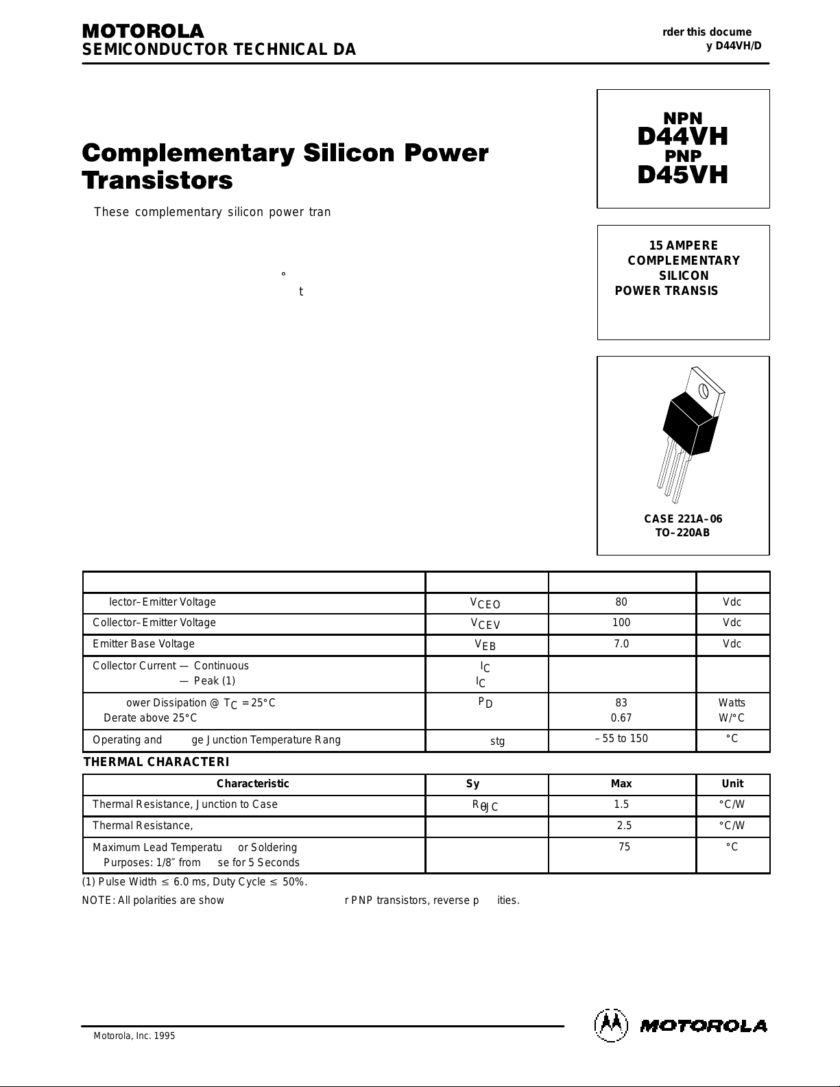
CASE 221A–06
TO–220AB
Page 2
2
Motorola Bipolar Power Transistor Device Data
ELECTRICAL CHARACTERISTICS (T
C
= 25_C unless otherwise noted)
Characteristic
Symbol
Min
Typ
Max
ÎÎÎ
ÎÎÎ
ÎÎÎ
Unit
OFF CHARACTERISTICS
Collector–Emitter Sustaining Voltage (1)
(IC = 25 mAdc, IB = 0)
V
CEO(sus)
80
—
—
ÎÎÎ
ÎÎÎ
ÎÎÎ
ÎÎÎ
Vdc
Collector–Emitter Cutoff Current
(VCE = Rated V
CEV
, V
BE(off)
= 4.0 Vdc)
(VCE = Rated V
CEV
, V
BE(off)
= 4.0 Vdc, TC = 100_C)
I
CEV
—
—
—
—
10
100
ÎÎÎ
ÎÎÎ
ÎÎÎ
ÎÎÎ
µAdc
Emitter Base Cutoff Current
(VEB = 7.0 Vdc, IC = 0)
I
EBO
—
—
10
ÎÎÎ
ÎÎÎ
ÎÎÎ
ÎÎÎ
µAdc
ON CHARACTERISTICS (1)
DC Current Gain
(IC = 2.0 Adc, VCE = 1.0 Vdc)
(IC = 4.0 Adc, VCE = 1.0 Vdc)
h
FE
35
20
—
—
—
—
ÎÎÎ
ÎÎÎ
ÎÎÎ
ÎÎÎ
ÎÎÎ
—
Collector–Emitter Saturation Voltage
(IC = 8.0 Adc, IB = 0.4 Adc) D44VH10
(IC = 8.0 Adc, IB = 0.8 Adc) D45VH10
(IC = 15 Adc, IB = 3.0 Adc, TC = 100_C) D44VH10
D45VH10
V
CE(sat)
—
—
—
—
—
—
—
—
0.4
1.0
0.8
1.5
ÎÎÎ
ÎÎÎ
ÎÎÎ
ÎÎÎ
ÎÎÎ
ÎÎÎ
Vdc
Base–Emitter Saturation Voltage
(IC = 8.0 Adc, IB = 0.4 Adc) D44VH10
(IC = 8.0 Adc, IB = 0.8 Adc) D45VH10
(IC = 8.0 Adc, IB = 0.4 Adc, TC = 100_C) D44VH10
(IC = 8.0 Adc, IB = 0.8 Adc, TC = 100_C) D45VH10
V
BE(sat)
—
—
—
—
—
—
—
—
1.2
1.0
1.1
1.5
ÎÎÎ
ÎÎÎ
ÎÎÎ
ÎÎÎ
ÎÎÎ
Vdc
DYNAMIC CHARACTERISTICS
Current Gain Bandwidth Product
(IC = 0.1 Adc, VCE = 10 Vdc, f = 20 MHz)
f
T
—
50
—
ÎÎÎ
ÎÎÎ
ÎÎÎ
ÎÎÎ
MHz
Output Capacitance
(VCB = 10 Vdc, IC = 0, f
test
= 1.0 MHz) D44VH10
D45VH10
C
ob
—
—
120
275
—
—
ÎÎÎ
ÎÎÎ
ÎÎÎ
ÎÎÎ
ÎÎÎ
pF
SWITCHING CHARACTERISTICS
Delay Time
t
d
—
—
50
ÎÎÎ
ÎÎÎ
ÎÎÎ
Rise Time
t
r
—
—
250
ÎÎÎ
ÎÎÎ
ÎÎÎ
Storage Time
CC
= 20 Vdc, IC = 8.0 Adc,
IB1 = IB2 = 0.8 Adc)
t
s
—
—
700
ÎÎÎ
ÎÎÎ
ÎÎÎ
Fall Time
t
f
—
—
90
ÎÎÎ
ÎÎÎ
ÎÎÎ
(1) Pulse Test: Pulse Width v 300 µs, Duty Cycle v 2%.
(VCC = 20 Vdc, IC = 8.0 Adc,
ns
Page 3

3
Motorola Bipolar Power Transistor Device Data
PACKAGE DIMENSIONS
CASE 221A–06
TO–220AB
ISSUE Y
NOTES:
1. DIMENSIONING AND TOLERANCING PER ANSI
Y14.5M, 1982.
2. CONTROLLING DIMENSION: INCH.
3. DIMENSION Z DEFINES A ZONE WHERE ALL
BODY AND LEAD IRREGULARITIES ARE
ALLOWED.
STYLE 1:
PIN 1. BASE
2. COLLECTOR
3. EMITTER
4. COLLECTOR
DIM MIN MAX MIN MAX
MILLIMETERSINCHES
A 0.570 0.620 14.48 15.75
B 0.380 0.405 9.66 10.28
C 0.160 0.190 4.07 4.82
D 0.025 0.035 0.64 0.88
F 0.142 0.147 3.61 3.73
G 0.095 0.105 2.42 2.66
H 0.110 0.155 2.80 3.93
J 0.018 0.025 0.46 0.64
K 0.500 0.562 12.70 14.27
L 0.045 0.060 1.15 1.52
N 0.190 0.210 4.83 5.33
Q 0.100 0.120 2.54 3.04
R 0.080 0.110 2.04 2.79
S 0.045 0.055 1.15 1.39
T 0.235 0.255 5.97 6.47
U 0.000 0.050 0.00 1.27
V 0.045 ––– 1.15 –––
Z ––– 0.080 ––– 2.04
B
Q
H
Z
L
V
G
N
A
K
F
1 2 3
4
D
SEATING
PLANE
–T–
C
S
T
U
R
J
Page 4

4
Motorola Bipolar Power Transistor Device Data
How to reach us:
USA /EUROPE: Motorola Literature Distribution; JAPAN: Nippon Motorola Ltd.; Tatsumi–SPD–JLDC, Toshikatsu Otsuki,
P.O. Box 20912; Phoenix, Arizona 85036. 1–800–441–2447 6F Seibu–Butsuryu–Center, 3–14–2 Tatsumi Koto–Ku, Tokyo 135, Japan. 03–3521–8315
MFAX: RMFAX0@email.sps.mot.com – TOUCHTONE (602) 244–6609 HONG KONG: Motorola Semiconductors H.K. Ltd.; 8B Tai Ping Industrial Park,
INTERNET: http://Design–NET.com 51 Ting Kok Road, Tai Po, N.T., Hong Kong. 852–26629298
Motorola reserves the right to make changes without further notice to any products herein. Motorola makes no warranty , representation or guarantee regarding
the suitability of its products for any particular purpose, nor does Motorola assume any liability arising out of the application or use of any product or circuit,
and specifically disclaims any and all liability, including without limitation consequential or incidental damages. “T ypical” parameters can and do vary in different
applications. All operating parameters, including “T ypicals” must be validated for each customer application by customer’s technical experts. Motorola does
not convey any license under its patent rights nor the rights of others. Motorola products are not designed, intended, or authorized for use as components in
systems intended for surgical implant into the body, or other applications intended to support or sustain life, or for any other application in which the failure of
the Motorola product could create a situation where personal injury or death may occur. Should Buyer purchase or use Motorola products for any such
unintended or unauthorized application, Buyer shall indemnify and hold Motorola and its officers, employees, subsidiaries, affiliates, and distributors harmless
against all claims, costs, damages, and expenses, and reasonable attorney fees arising out of, directly or indirectly, any claim of personal injury or death
associated with such unintended or unauthorized use, even if such claim alleges that Motorola was negligent regarding the design or manufacture of the part.
Motorola and are registered trademarks of Motorola, Inc. Motorola, Inc. is an Equal Opportunity/Affirmative Action Employer.
D44VH/D
*D44VH/D*
◊
 Loading...