

Page 1
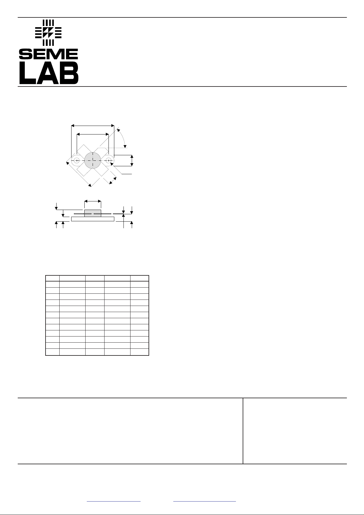
MECHANICAL DATA
TetraFET
D1002UK
METAL GATE RF SILICON FET
GOLD METALLISED
HJ
PIN 1 SOURCE
PIN 3 SOURCE
DIM mm Tol. Inches Tol.
A 24.76 0.13 0.975 0.005
B 18.42 0.13 0.725 0.005
C 45° 5° 45° 5°
D 6.35 0.13 0.25 0.005
E 3.17 0.13 0.125 DIA 0.005
F 5.71 0.13 0.225 0.005
G 9.52 0.13 0.375 0.005
H 6.60 REF 0.260 REF
I 0.13 0.02 0.005 0.001
J 4.32 0.13 0.170 0.005
K 2.54 0.13 0.100 0.005
M 20.32 0.25 0.800 0.010
A
B
C
MULTI-PURPOSE SILICON
DMOS RF FET
12
D
34
M
G
E
F
FEATURES
• SIMPLIFIED AMPLIFIER DESIGN
K
I
• SUITABLE FOR BROAD BAND APPLICATIONS
DA
PIN 2 DRAIN
PIN 4 GATE
•LOW C
• SIMPLE BIAS CIRCUITS
• LOW NOISE
• HIGH GAIN – 16 dB MINIMUM
APPLICATIONS
• HF/VHF/UHF COMMUNICATIONS
from 1 MHz to 175 MHz
40W – 28V – 175MHz
SINGLE ENDED
rss
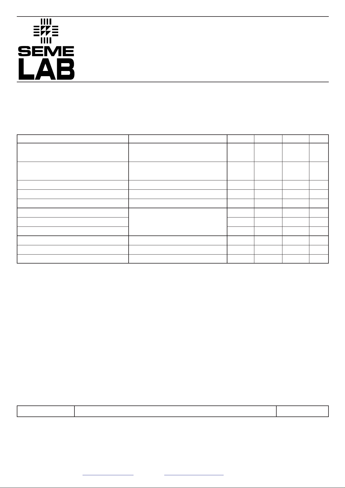
ABSOLUTE MAXIMUM RATINGS (T
P
D
BV
BV
I
D(sat)
T
stg
T
j
DSS
GSS
Power Dissipation
Drain – Source Breakdown Voltage
Gate – Source Breakdown Voltage
Drain Current
Storage Temperature
Maximum Operating Junction Temperature
= 25°C unless otherwise stated)
case
Semelab plc. Telephone +44(0)1455 556565. Fax +44(0)1455 552612.
E-mail: sales@semelab.co.uk
Website: http://www.semelab.co.uk
87W
70V
±20V
10A
–65 to 150°C
200°C
3/99
Page 2
D1002UK
ELECTRICAL CHARACTERISTICS (T
= 25°C unless otherwise stated)
case
Parameter Test Conditions Min. Typ. Max. Unit
BV
I
DSS
I
GSS
V
GS(th)
g
fs
G
PS
η Drain Efficiency
VSWR Load Mismatch Tolerance
C
iss
C
oss
C
rss
* Pulse Test: Pulse Duration = 300 µs , Duty Cycle ≤ 2%
Drain–Source
DSS
Breakdown Voltage
Zero Gate Voltage
Drain Current
Gate Leakage Current
Gate Threshold Voltage*
Forward Transconductance*
Common Source Power Gain
Input Capacitance
Output Capacitance
Reverse Transfer Capacitance
VGS= 0 ID= 100mA
VDS= 28V VGS= 0
VGS= 20V VDS= 0
ID= 10mA VDS= V
VDS= 10V ID= 2A
PO= 40W
VDS= 28V IDQ= 0.2A
f = 175MHz
VDS= 28V VGS= –5V f = 1MHz
VDS= 28V VGS= 0 f = 1MHz
VDS= 28V VGS= 0 f = 1MHz
GS
70
2
1
17
1.6
16
50
20:1
120
60
5
V
mA
µA
V
S
dB
%
—
pF
pF
pF
HAZARDOUS MATERIAL WARNING
The ceramic portion of the device between leads and metal flange is beryllium oxide. Beryllium oxide dust is highly
toxic and care must be taken during handling and mounting to avoid damage to this area.
THESE DEVICES MUST NEVER BE THROWN AWAY WITH GENERAL INDUSTRIAL OR DOMESTIC WASTE.
THERMAL DATA
R
THj–case
Thermal Resistance Junction – Case Max. 2.0°C / W
Semelab plc. Telephone +44(0)1455 556565. Fax +44(0)1455 552612.
E-mail: sales@semelab.co.uk
Website: http://www.semelab.co.uk
3/99
Page 3

D1002UK
80
70
60
50
P
out
40
W
30
20
10
0
0 1 2 3 4 5 6 7 8
f1= 175.0MHz
Idq= 0.2A
VDS= 28V
P
W
in
Pout
Drain Efficiency
80
70
60
50
Drain Efficiency
40
%
30
20
10
0
Figure 1 – Power Output and Efficiency
vs. Power Input.
-10
-15
-20
-25
IMD3
-30
dBc
-35
-40
-45
-50
0 5 10 15 20 25 30 35 40 45 50 55 60 65
P
out
W PEP
f1= 175.0MHz
f2= 175.1MHz
VDS= 28V
Idq = 0.2A
Idq = 1A
80
70
60
50
P
out
40
W
30
20
10
0
0 1 2 3 4 5 6 7 8
Pout
Gain
P
W
in
f1= 175.0MHz
Idq= 0.2A
VDS= 28V
17
17
16
16
15
15
14
14
Gain
13
13
dB
12
12
11
11
10
10
9
9
Figure 2 – Power Output & Gain
vs. Power Input.
D1002UK
OPTIMUM SOURCE AND LOAD IMPEDANCE
Frequency Z
S
MHz ΩΩ
175MHz 3.8 + j6.5 4.6 + j0.4
Z
L
Figure 3 – IMD vs. Output Power.
Typical S Parameters
! Vds=28V Idq=0.2A
# MHZ S MA R 50
!Freq S11 S21 S12 S22
MHz mag ang mag ang mag ang mag ang
50 0.76 -144 15.6 86 0.026 1 0.58 -119
100 0.79 -155 7.1 61 0.021 -9 0.66 -132
150 0.84 -163 4.2 43 0.012 -3 0.74 -144
200 0.87 -169 2.7 33 0.009 47 0.81 -154
250 0.90 -176 1.9 23 0.016 76 0.85 -163
300 0.92 177 1.5 20 0.025 87 0.88 -172
350 0.94 170 1.1 11 0.033 85 0.91 -180
400 0.96 163 0.9 6 0.046 82 0.94 172
450 0.97 156 0.7 -2 0.051 78 0.96 165
500 0.98 150 0.6 -8 0.062 76 0.98 157
550 0.98 144 0.4 -12 0.068 74 0.98 152
600 0.98 141 0.4 -14 0.078 67 0.98 148
Semelab plc. Telephone +44(0)1455 556565. Fax +44(0)1455 552612.
E-mail: sales@semelab.co.uk
Website: http://www.semelab.co.uk
3/99
Page 4

D1002UK
T1 10mm
T2 13mm
T3 12mm
T4 4mm
15
Gate-Bias
10-30pF
T1 T2
10-30pF
10K
10nF
10K
L1
9 x 6mm
contact
pad
D1001UK
9 x 6 mm
contact pad
L4
L2
T3
4.7pF
D1002UK 175MHz TEST FIXTURE
Substrate 1.6mm PTFE/glass, Er=2.5
All microstrip lines W=4.4mm
L1 1.5 turns 22swg enamelled copper wire, 6mm i.d.
L2 10 turns 19swg enamelled copper wire, 6mm i.d.
L3 1.5 turns 22swg enamelled copper wire, 6mm i.d.
L4 13.5 turns 19swg enamelled copper wire on
Siemens B64920A618X830 ferrite core
+28V
10nF
L3
T4
1nF100nF
10uF
16-100pF
16-100pF
Semelab plc. Telephone +44(0)1455 556565. Fax +44(0)1455 552612.
E-mail: sales@semelab.co.uk
Website: http://www.semelab.co.uk
3/99
 Loading...