

Page 1

Description
The CXP85840A/85848A/85856A are the CMOS 8-bit
microcomputer integrating on a single chip an A/D
converter, serial interface, timer/counter, time-base
timer, closed caption decoder, data slicer, on-screen
display function, I2C bus interface, PWM output,
remote control reception circuit, HSYNC counter and
watchdog timer, besides the basic configurations of
8-bit CPU, ROM, RAM, I/O ports.
The CXP85840A/85848A/85856A also provide a
power-on reset function and sleep function that
enables to lower the power consumption.
Features
• A wide instruction set (213 instructions) which covers
various types of data
– 16-bit operation/multiplication and division/Boolean bit operation instructions
• Minimum instruction cycle 333ns at 12MHz operation
• Incorporated ROM 40K bytes (CXP85840A)
48K bytes (CXP85848A)
56K bytes (CXP85856A)
• Incorporated RAM 2176 bytes (Excludes closed caption decoder and VRAM for on-screen display)
• Peripheral functions
– A/D converter 8-bit 6-channel successive approximation method
(Conversion time of 26.7µs at 12MHz)
– Serial interface 8-bit clock sync type, 1 channel
– Timer 8-bit timer
8-bit timer/counter
19-bit time-base timer
– Closed caption decoder Data slicer
Corresponds to FCC (EDS supported), 8 × 13 dots, 192 character types
15 character colors, 4 lines × 34 characters
frame background 15 colors/ half blanking
italic, underline, vertical scrolling
– On-screen display (OSD) function 12 × 16 dots, 192 character types, 15 character colors
2 lines × 24 characters
frame background 8 colors/ half blanking
background on full screen 15 colors/ half blanking
edging and vertical scrolling for every line
jitter elimination circuit
sprite OSD, 12 × 16 dots, 1 screen, 8 colors for every dot
– I2C bus interface
– PWM output 8 bits, 8 channels
– Remote control reception circuit 8-bit pulse measurement counter, 6-stage FIFO
– HSYNC counter 2 channels
– Watchdog timer
• Interruption 15 factors, 15 vectors, multi-interruption possible
• Standby mode Sleep
• Package 64-pin plastic SDIP/QFP
• Piggyback/evaluator CXP85890A 64-pin ceramic PSDIP (Supports custom font)
Perchase of Sony's I2C components conveys a licence under the Philips I2C Patent Rights to use these components
in an I2C system, provided that the system conforms to the I2C Standard Specifications as defined by Philips.
– 1 –
CXP85840A/85848A/85856A
E97739A86
CMOS 8-bit Single Chip Microcomputer
Sony reserves the right to change products and specifications without prior notice. This information does not convey any license by
any implication or otherwise under any patents or other right. Application circuits shown, if any, are typical examples illustrating the
operation of the devices. Sony cannot assume responsibility for any problems arising out of the use of these circuits.
64 pin SDIP (Plastic) 64 pin QFP (Plastic)
Structure
Silicon gate CMOS IC
Page 2
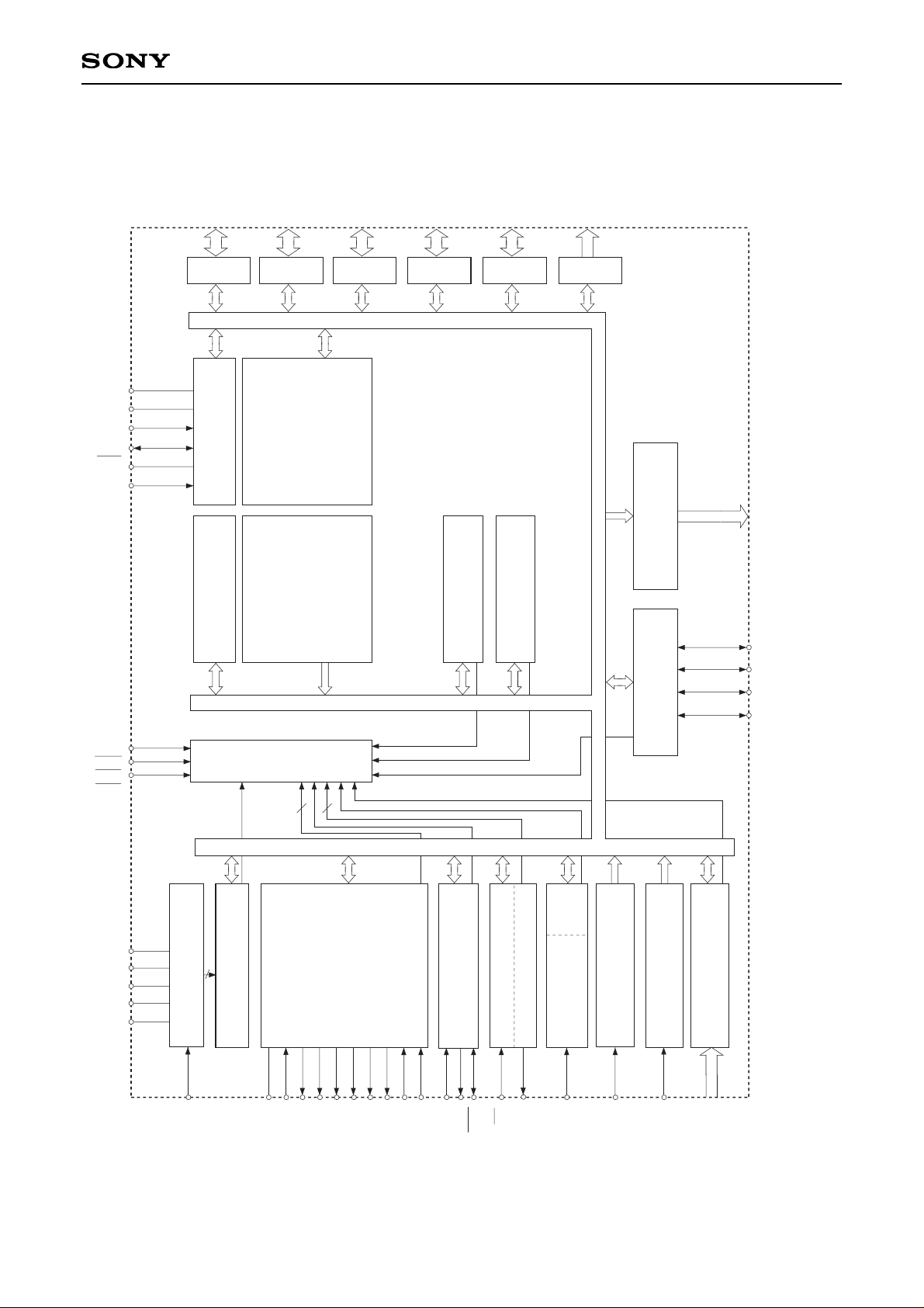
– 2 –
CXP85840A/85848A/85856A
VIN
XLC
EXLC
R
G
B
I
YS
YM
HSYNC
VSYNC
SI
SO
SCK
EC
TO
RMC
HSC0
HSC1
AN0 to AN5
CVss
CV
DD
Cap
LFC2
DATA SLICER
CC DECODER
ON SCREEN DISPLAY
SERIAL INTERFACE UNIT
8BIT TIMER/COUNTER 0
REMOCON
HSYNC COUNTER 0
HSYNC COUNTER 1
A/D CONVERTER
FIFO
3
2
INT2
INT1
INT0
SCL1
SCL0
SDA1
SDA0
I
2
C BUS
INTERFACE UNIT
8BIT PWM
WATCHDOG TIMER
PRESCALER/
TIME BASE TIMER
SPC700 CPU CORE
ROM
40K/48K/56K BYTES
CLOCK GENERATOR/
SYSTEM CONTROL
RAM
2176 BYTES
Vss
V
DD
MP
RST
XTAL
EXTAL
PWM0 to PWM7
PORT A
PA0 to PA7
8
PB0 to PB6
7
PC0 to PC7
8
PD0 to PD7
8
PE0 to PE2
3
PF0 to PF7
8
INTERRUPT CONTROLLER
PORT BPORT CPORT DPORT EPORT F
8BIT TIMER 1
2
LFC1
8
6
Block Diagram
Page 3
– 3 –
CXP85840A/85848A/85856A
2
3
4
5
6
7
8
9
10
11
12
13
14
15
16
17
18
19
20
21
22
23
24
25
26
27
28
29
30
31
32
1
40
39
38
37
36
35
34
33
41
42
43
44
45
46
47
48
49
50
51
52
53
54
55
56
57
58
59
60
63
64
61
62
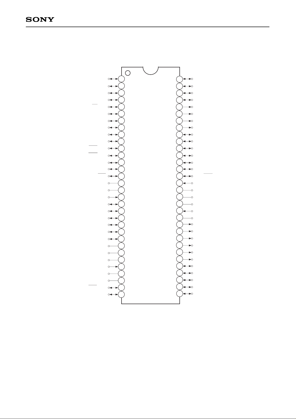
PC3
PC2
PC1
PC0
EC/PD7
RMC/PD6
HS1/PD5
HS0/PD4
SI/ PD3
SO/PD2
SCK/PD1
INT2/PD0
HSYNC/PA7
VSYNC/PA6
RST
Vss
XTAL
EXTAL
PA5/AN5
PA4/AN4
PA3/AN3
PA2/AN2
PA1/AN1
PA0/AN0
CVss
LFC2
LFC1
VIN
CV
DD
Cap
INT1/PB6
PB5
PC4
PC5
PC6
PC7
PF0/PWM0
PF1/PWM1
PF2/PWM2
PF3/PWM3
PF4/SCL0/PWM4
PF5/SCL1/PWM5
PF6/SDA0/PWM6
PF7/SDA1/PWM7
PE0/TO
PE1
PE2/INT0
MP
Vss
V
DD
NC
EXLC
XLC
YM
YS
I
B
G
R
PB0
PB1
PB2
PB3
PB4
Note)
1. NC (Pin 46) is always connected to VDD.
2. Vss (Pins 16 and 48) are both connected to GND.
3. MP (Pin 49) is always connected to GND.
Pin Assignment (Top View) 64-pin SDIP
Page 4
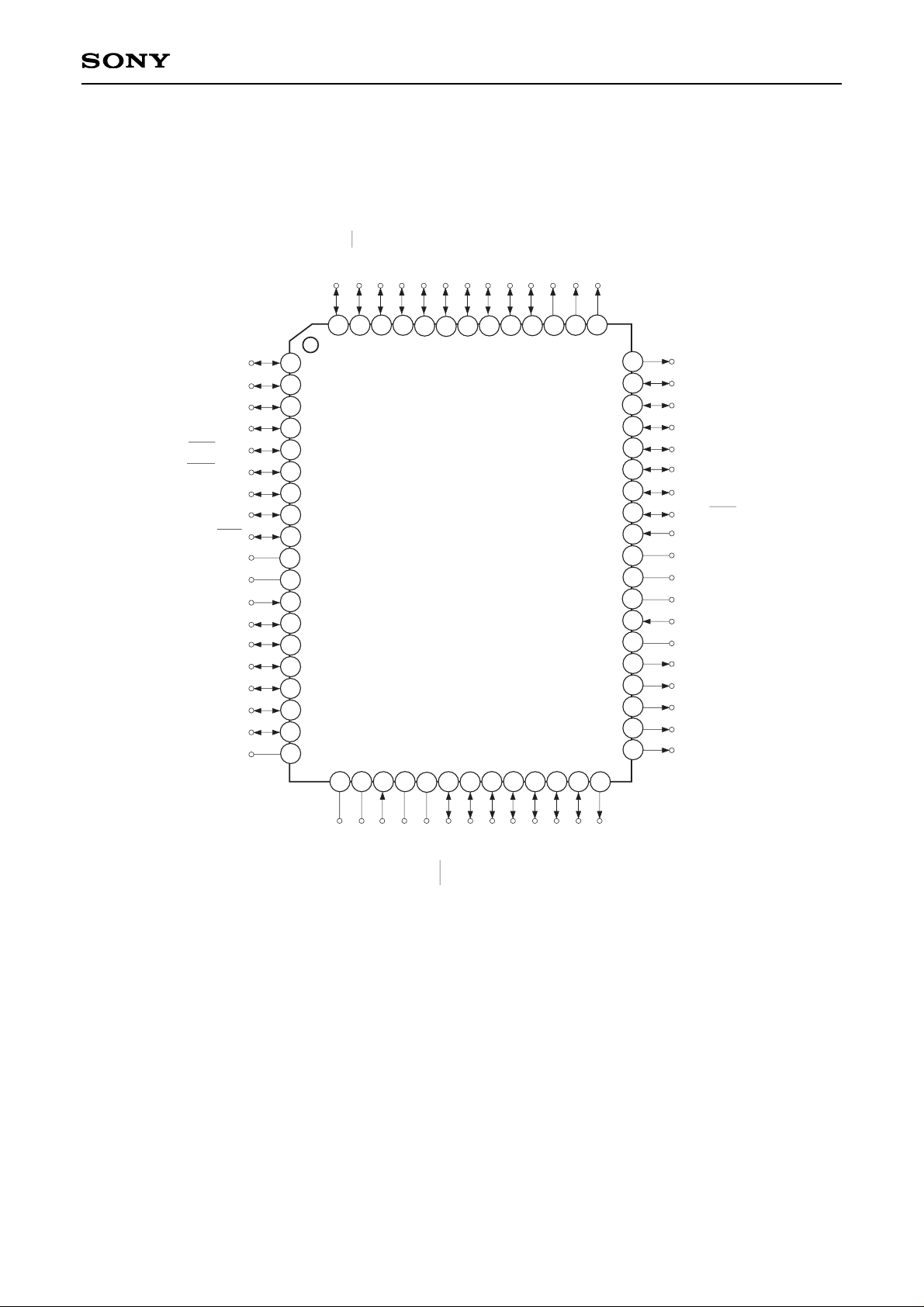
– 4 –
CXP85840A/85848A/85856A
Note)
1. NC (Pin 40) is always connected to VDD.
2. Vss (Pins 10 and 42) are both connected to GND.
3. MP (Pin 43) is always connected to GND.
HS1/PD5
HS0/PD4
SI/PD3
SO/PD2
SCK/PD1
INT2/PD0
HSYNC/PA7
VSYNC/PA6
RST
Vss
XTAL
EXTAL
PA5/AN5
PA4/AN4
PA3/AN3
PA2/AN2
PA1/AN1
PA0/AN0
CVss
2
3
4
5
6
7
8
9
10
11
12
13
14
15
16
17
18
19
1
PF3/PWM3
PF4/SCL0/PWM4
PF5/SCL1/PWM5
PF6/SDA0/PWM6
PF7/SDA1/PWM7
PE0/TO
PE1
PE2/INT0
MP
Vss
V
DD
NC
EXLC
XLC
YM
YS
I
B
G
40
39
38
37
36
35
34
33
41
42
43
44
45
46
47
48
49
50
51
PD6/RMC
PD7/EC
PC0
PC1
PC2
PC3
PC4
PC5
PC6
PC7
PF0/PWM0
PF1/PWM1
PF2/PWM2
52
53
54
55
56
57
58
59
60
63
64
61
62
LFC2
LFC1
VIN
CV
DD
Cap
INT1/PB6
PB5
PB4
PB3
PB2
PB1
PB0
R
20
21
22
23
24
25
26
27
28
29
30
31
32
Pin Assignment (Top View) 64-pin QFP
Page 5
– 5 –
CXP85840A/85848A/85856A
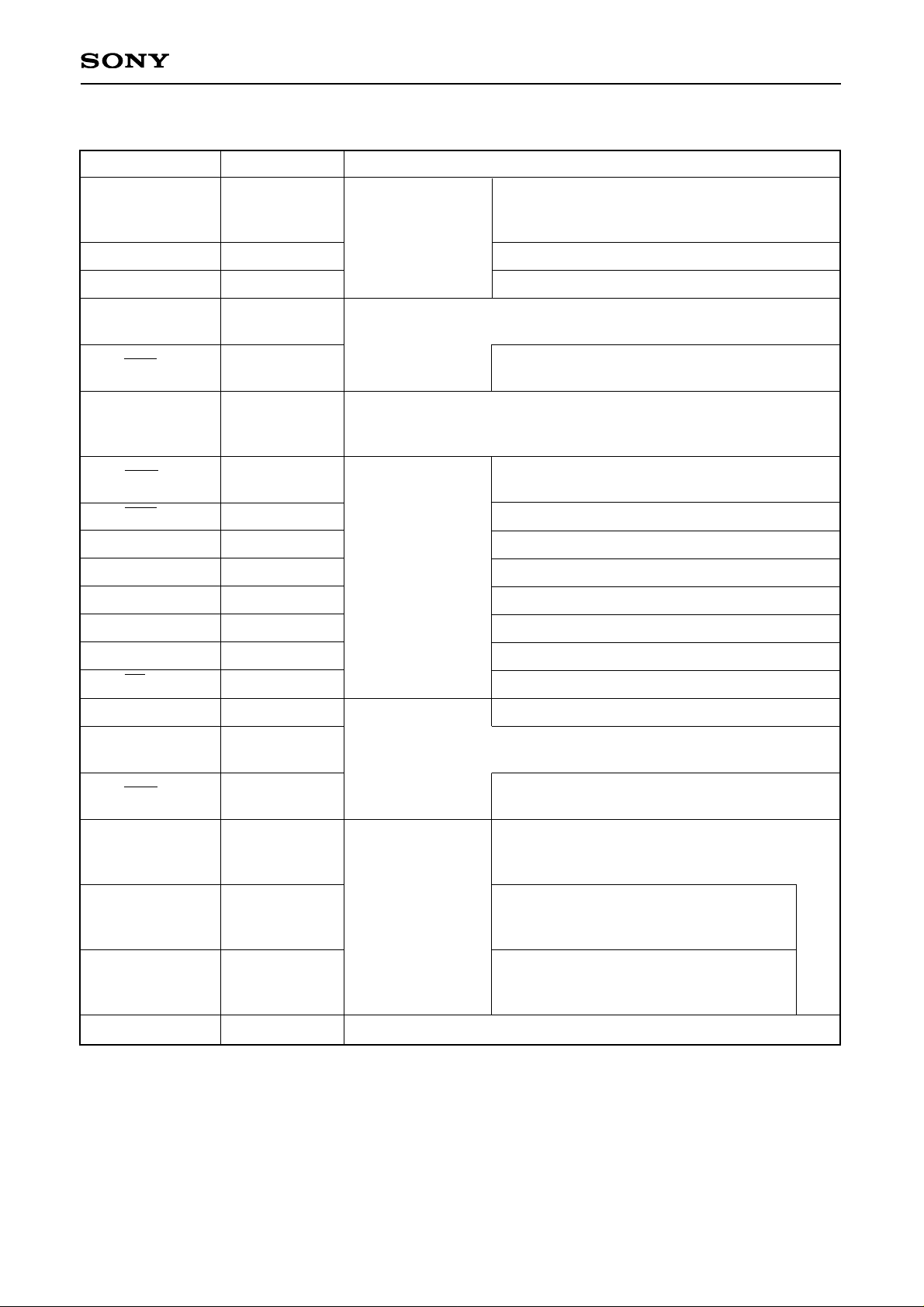
(Port A)
8-bit I/O port. I/O
can be set in a unit
of single bits.
(8 pins)
(Port B)
7-bit I/O port. I/O can be set in a unit of single bits.
(7 pins)
(Port C)
8-bit I/O port. I/O can be set in a unit of single bits.
(8 pins)
(Port D)
8-bit I/O port.
I/O can be set in a
unit of single bits.
Can drive 12mA
synk current.
(8 pins)
(Port E)
3-bit I/O port.
I/O can be set in a
unit of single bits.
(3 pins)
(Port F)
8-bit output port
and large current
(12mA) N-channel
open drain output.
Lower 4 bits are
medium drive voltage
(12V); upper 4 bits
are 5V drive.
(8 pins)
6-bit OSD display output. (6 pins)
Pin Description
Symbol
PA0/AN0
to
PA5/AN5
PA6/VSYNC
PA7/HSYNC
PB0 to PB5
PB6/INT1
PC0 to PC7
PD0/INT2
PD1/SCK
PD2/SO
PD3/SI
PD4/HS0
PD5/HS1
PD6/RMC
PD7/EC
PE0/TO
PE1
PE2/INT0
PF0/PWM0
to
PF3/PWM3
PF4/SCL0/PWM4
PF5/SCL1/PWM5
PF6/SDA0/PWM6
PF7/SDA1/PWM7
R, G, B, I, YS, YM
I/O/
Analog input
I/O/Input
I/O/Input
I/O
I/O/Input
I/O
I/O/Input
I/O/I/O
I/O/Output
I/O/Input
I/O/Input
I/O/Input
I/O/Input
I/O/Input
I/O/Output
I/O
I/O/Input
Output/Output
Output/I/O
Output/I/O
Output
I/O
Description
Analog inputs to A/D converter.
(6 pins)
OSD display vertical sync signal input.
OSD display horizontal sync signal input.
External interruption request input.
Active at the falling edge.
External interruption request input.
Active at the falling edge.
Serial clock I/O.
Serial data output.
Serial data input.
HSYNC counter (CH0) input.
HSYNC counter (CH1) input.
Remote control reception circuit input.
External event input for timer/counter.
Rectangular wave output for timer/counter
External interruption request input.
Active at the falling edge.
8-bit PWM output. (8 pins)
I2C bus interface transfer clock I/O.
(2 pins)
I2C bus interface transfer data I/O.
(2 pins)
Page 6
– 6 –
CXP85840A/85848A/85856A
Symbol
EXLC
XLC
VIN
Cap
LFC1, LFC2
CVDD
CVss
EXTAL
XTAL
RST
MP
NC
VDD
Vss
Input
Output
Input
—
—
Input
Output
I/O
Input
OSD display clock oscillation I/O.
Oscillation frequency is determined by the external L and C.
External composite video signal input.
Input the 2Vp-p signal via a capacitor.
Connects a data slicer capacitor between Cap and CVss.
Connects a low-pass filter capacitor for PLL circuit between LFC1 and
LFC2.
Positive power supply for data slicer.
GND for data slicer.
Connects a crystal for system clock oscillation. When a clock is
supplied externally, input it to EXTAL and leave XTAL open.
System reset; active at Low level. I/O pin. Outputs a Low level when the
power is turned on and the internal power-on reset function operates.
(Mask option)
Test mode pin. Always connect to GND.
No connected.
Under normal operation, connect to VDD.
Positive power supply.
GND. Connect two Vss pins to GND.
I/O Description
Page 7
– 7 –
CXP85840A/85848A/85856A
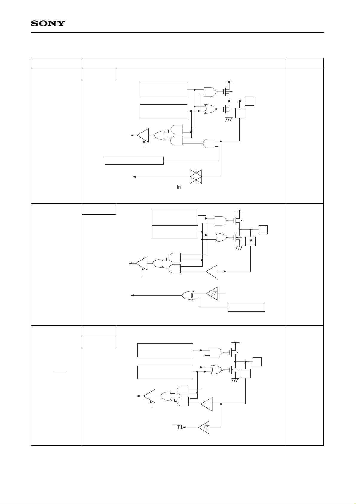
Input/Output Circuit Formats for Pins
Port A
Port A
Port B
Port C
2 pins
6 pins
15 pins
Hi-Z
Hi-Z
Hi-Z
Pin When resetCircuit format
PA0/AN0
to
PA5/AN5
PB0 to PB5
PB6/INT1
PC0 to PC7
PA6/VSYNC
PA7/HSYNC
Data bus
RD (Port A)
Port A function selection
“0” when reset
A/D converter
Port A data
Port A direction
“0” when reset
Port A data
Port A direction
“0” when reset
Input multiplexer
IP
Input
protection
circuit
IP
VSYNC, HSYNC
Data bus
Data bus
RD (Port A)
Ports B, C data
Ports B, C direction
“0” when reset
RD (Ports B, C)
Schmitt input
Input polarity
“0” when reset
IP
Schmitt input
INT1
Page 8

– 8 –
CXP85840A/85848A/85856A
Port D
Port D
Port E
6 pins
2 pins
3 pins
Hi-Z
Hi-Z
PE0, PE1:
High level
PE2: Hi-Z
PD1/SCK
PD2/SO
PE0/TO
PE1
PE2/INT0
PD0/INT2
PD3/SI
PD4/HS0
PD5/HS1
PD6/RMC
PD7/EC
Pin When resetCircuit format
Data bus
INT2, SI, HS0, HS1, RMC, EC
Serial output enable
Port D data
Port D direction
“0” when reset
RD (Port D)
SCK, SO
Port D data
Port D direction
“0” when reset
Schmitt input
∗
Large current 12mA
∗
IP
∗
IP
Data bus
RD (Port D)
SCK only
TO
Port E function
selection
“1” when reset
Port E data
“1” when reset for PE0 and 1
Port E direction
“1” when reset for PE0 and 1
“0” when reset for PE2
Data bus
RD (Port E)
INT0
Schmitt input
∗
Large current 12mA
Schmitt input
only for PE2
IP
Page 9

– 9 –
CXP85840A/85848A/85856A
Port F
Port F
4 pins
4 pins
6 pins
2 pins
PF4/PWM4/SCL0
PF5/PWM5/SCL1
PF6/PWM6/SDA0
PF7/PWM7/SDA1
Hi-Z
Hi-Z
Hi-Z
Oscillation
halted
R
G
B
I
YS
YM
PF0/PWM0
to
PF3/PWM3
EXLC
XLC
R, G, B, I, YS, YM
Writing data to output
polarity register brings
output to active.
Output polarity
“0” when reset
Oscillation control
EXLC
IP
OSC display clock
IP
XLC
Pin When resetCircuit format
PWM0 to PWM3
Port F data
“1” when reset
Port F function
selection
“0” when reset
I2C output enable
PWM4 to PWM7
Port F data
“1” when reset
Port F function
selection
“0” when reset
SCL, SDA
(I2C circuit)
SCL, SDA
Schmitt input
∗
∗
12V drive voltage
Large current 12mA
∗
IP
BUS SW
2
To other I
(SCL1 for SCL0)
∗
Large current 12mA
C pins
Page 10

– 10 –
CXP85840A/85848A/85856A
2 pins
1 pin
RST
Oscillation
Low level
EXTAL
XTAL
IP
EXTAL
XTAL
• Diagram shows the circuit
composition during oscillation.
• Feedback resistor is removed
during stop mode. (This device
does not enter the stop mode.)
Schmitt input
Pull-up resistor
From power-on reset circuit
(Mask option)
Mask option
OP
Pin When resetCircuit format
Page 11

– 11 –
CXP85840A/85848A/85856A
∗1
VIN and VOUT should not exceed VDD + 0.3V.
∗2
The large current output port is Port D (PD) and Port F (PF).
Note) Usage exceeding absolute maximum ratings may permanently impair the LSI. Normal operation should
be conducted under the recommended operating conditions. Exceeding those conditions may
adversely affect the reliability of the LSI.
VDD
VIN
VOUT
VOUTP
IOH
∑IOH
IOL
IOLC
∑IOL
Topr
Tstg
PD
–0.3 to +7.0
–0.3 to +7.0
∗1
–0.3 to +7.0
∗1
–0.3 to +15.0
–5
–50
15
20
100
–20 to +75
–55 to +150
1000
600
V
V
V
V
mA
mA
mA
mA
mA
°C
°C
mW
mW
PF0 to PF3 pins
Total of all output pins
Ports excluding large current outputs
(value per pin)
Large current output ports
(value per pin∗2)
Total of all output pins
SDIP-64P-01
GFP-64P-L01
Item Symbol Ratings Unit Remarks
Absolute Maximum Ratings (Vss = 0V reference)
Supply voltage
Data slicer supply voltage
High level input voltage
Low level input voltage
Operating temperature
5.5
5.5
5.5
5.5
VDD
VDD
VDD + 0.3
0.3VDD
0.2VDD
0.4
+75
V
V
V
V
V
V
V
V
V
V
°C
Item Symbol Min. Max. Unit Remarks
4.5
3.5
2.5
4.5
0.7VDD
0.8VDD
VDD – 0.4
0
0
–0.3
–20
CVDD
VIH
VIHS
VIHEX
VIL
VILS
VILEX
Topr
Guaranteed operation range for 1/2 and
1/4 frequency dividing clocks
Guaranteed operation range for 1/16
frequency dividing clock or sleep mode
Guaranteed data hold range for stop mode
∗1
∗5
∗2
∗3
EXTAL pin
∗4
∗2
∗3
EXTAL pin
∗4
VDD
∗1
This device does not enter the stop mode.
∗2
PA, PB, PC, PE0 to PE1, SCL0 to 1, SDA0 to 1 pins.
∗3
INT2, SCK, SO, SI, HS0, HS1, RMC, EC, INT1, HSYNC, VSYNC, RST pins.
∗4
Specifies only during external clock input.
∗5
CVDD and VDD should be set to the same voltage.
Recommended Operating Conditions (Vss = 0V reference)
Supply voltage
Input voltage
Output voltage
Medium drive output voltage
High level output current
High level total output current
Low level output current
Low level total output current
Operating temperature
Storage temperature
Allowable power dissipation
Page 12

– 12 –
CXP85840A/85848A/85856A
VDD = 4.5V, IOH = –0.5mA
VDD = 4.5V, IOH = –1.2mA
VDD = 4.5V, IOL = 1.8mA
VDD = 4.5V, IOL = 3.6mA
VDD = 4.5V, IOL = 3.0mA
VDD = 4.5V, IOL = 4.0mA
VDD = 5.5V, VIH = 5.5V
VDD = 5.5V, VIL = 0.4V
VDD = 4.5V, IOL = 12.0mA
High level output
voltage
Low level output
voltage
Input current
I/O leakage current
Open drain I/O
leakage current (in
N-ch Tr OFF state)
I2C bus switch
connection impedance
(in output Tr OFF state)
Supply current
Input capacitance
4.0
3.5
37
2.5
—
5.0
10
—
—
5
—
10.0
20
µA
mA
pF
50
10
120
50
mA
mA
µA
µA
Ω
0.4
0.6
1.5
0.4
0.6
40
–40
–400
±10
V
V
V
V
V
µA
µA
µA
µA
0.5
–0.5
–1.5
V
V
PA to PD, PE
R, G, B, I, YS, YM
PA to PD, PE
R, G, B, I, YS, YM,
PF0 to PF3, RST
∗1
PD, PF
PF4 to PF7
(SCL0, SCL1,
SDA0, SDA1)
EXTAL
RST
∗2
PA to PE, HSYNC,
VSYNC, R, G, B, I,
YS, YM, RST
∗2
PF0 to PF3
PF4 to PF7
SCL0: SCL1
SDA0: SDA1
VDD = 5.5V, VIL = 0.4V
VDD = 5.5V,
VI = 0, 5.5V
VDD = 5.5V, VOH = 12.0V
VDD = 5.5V, VOH = 5.5V
VDD = 4.5V
VSCL0 = VSCL1 = 2.25V
VSDA0 = VSDA1 = 2.25V
VDD
∗3
CVDD
Stop mode
∗4
VDD = 5.5V, termination of
12MHz oscillation
Sleep mode
VDD = 5.5V,
12MHz crystal oscillation
(C1 = C2 = 15pF)
PA to PE, SCL,
SDA,
EXLC, EXTAL,
VIN, RST
Clock 1MHz
0V for no-measured pins
Item Symbol Pins Conditions Min. Typ. Max. Unit
VOH
VOL
IIZ
ILOH
RBS
IDD
IDDSL
IDDST
ICVDD
CIN
IIHE
IIHL
IILR
Electrical Characteristics
DC characteristics (Ta = –20 to +75°C, Vss = 0V reference)
∗1
Specifies RST pin only when the power-on reset circuit is selected with mask option.
∗2
For RST pin, specifies the input current when pull-up resistor is selected, and specifies the leakage current
when non-resistor is selected.
∗3
When all output pins are left open. Specifies only when the OSD oscillation is halted.
∗4
This device does not enter the stop mode.
1/2 frequency dividing clock
operation VDD = 5.5V,
12MHz crystal oscillation
(C1 = C2 = 15pF)
VDD = 5.5V
Page 13

– 13 –
CXP85840A/85848A/85856A
12.0
200
20
AC Characteristics
(1) Clock timing
∗1
Indicates three values according to the contents of the clock control register (CLC: 00FEh) upper 2 bits
(CPU clock selection).
tsys (ns) = 2000/fc (Upper 2 bits = “00”), 4000/fc (Upper 2 bits = “01”), 16000/fc (Upper 2 bits = “11”)
37.5
tsys
∗1
+ 50
System clock frequency
System clock input pulse
width
System clock input rise
and fall times
Event count input clock
pulse width
Event count input clock
rise and fall times
fC
tXL,
tXH
tCR,
tCF
tEH,
tEL
tER,
tEF
XTAL
EXTAL
EXTAL
EXTAL
EC
EC
MHz
ns
ns
ns
ms
Item Symbol Pins Conditions Typ. Max. Unit
Fig. 1, Fig. 2
Fig. 1, Fig. 2
External clock drive
Fig. 1, Fig. 2
External clock drive
Fig. 3
Fig. 3
(Ta = –20 to +75°C, VDD = 4.5 to 5.5V, Vss = 0V reference)
Fig. 1. Clock timing
EXTAL
t
XH tXLtCF tCR
0.4V
V
DD – 0.4V
1/fc
Fig. 2. Clock applied conditions
A
A
Crystal oscillation
Ceramic oscillation
EXTAL
XTAL
External clock
EXTAL
XTAL
OPEN
C
1 C2
Fig. 3. Event count clock timing
EC
t
EH tELtEF tER
0.2VDD
0.8VDD
Min.
AAA
AAA
Page 14

– 14 –
CXP85840A/85848A/85856A
(2) Serial transfer (Ta = –20 to +75°C, VDD = 4.5 to 5.5V, Vss = 0V reference)
Item
SCK cycle time
tKCY
SCK
Input mode
Output mode
SCK input mode
SCK output mode
SCK input mode
SCK output mode
SCK input mode
SCK output mode
SCK input mode
SCK output mode
1000
8000/fc
400
4000/fc – 50
100
200
200
100
200
100
ns
ns
ns
ns
ns
ns
ns
ns
ns
ns
SCK
SI
SI
SO
tKH
tKL
tSIK
tKSI
tKSO
SCK High and Low level
widths
SI input setup time
(for SCK ↑)
SI hold time (for SCK ↑)
SCK ↓ → SO delay time
Symbol Pins Conditions Min. Max. Unit
Note) The load of SCK output mode and SO output delay time is 50 pF + 1TTL.
Fig. 4. Serial transfer timing
0.2VDD
0.8VDD
tKL tKH
SO
tKCY
tSIK
tKSI
0.2VDD
0.8VDD
tKSO
0.2VDD
0.8VDD
Output data
Input data
SI
SCK
Page 15

– 15 –
CXP85840A/85848A/85856A
Resolution
Linearity error
Zero transition
voltage
Full-scale transition
voltage
Conversion time
Sampling time
Analog input voltage
VZT
∗1
VFT
∗2
tCONV
tSAMP
VIAN AN0 to AN5
Ta = 25°C
VDD = 5.0V
Vss = 0V
–10
4910
160/fADC
∗3
12/fADC
∗3
0
10
4970
8
±3
70
5030
VDD
Bits
LSB
mV
mV
µs
µs
V
Item Symbol Pins Conditions Min. Typ. Max. Unit
(3) A/D converter (Ta = –20 to +75°C, VDD = 4.5 to 5.5V, Vss = 0V reference)
Linearity error
VZT VFT
Analog input
FF
h
FEh
01h
00h
Digital conversion value
Fig. 5. Definitions of A/D converter terms
00 (φ = fEX/2)
01 (φ = fEX/4)
11 (φ = fEX/16)
fADC = fC/2
fADC = fC/4
fADC = fC/16
fADC = fC
CKS
PCK1, 0
0 (φ/2 selection) 1 (φ selection)
fADC = fC/2
fADC = fC/8
∗1
VZT:Value at which the digital conversion value changes
from 00H to 01H and vice versa.
∗2
VFT:Value at which the digital conversion value changes
from FEh to FFh and vice versa.
∗3
fADC indicates the below values due to the contents of bit
6 (CKS) of the A/D control register (ADC: 00F9h) and bits
7 (PCK1) and 6 (PCK0) of the clock control register
(CLC: 00FEh).
Page 16

– 16 –
CXP85840A/85848A/85856A
External interruption High
and Low level widths
Reset input Low level width
INT0
INT1
INT2
RST
1
32/fc
µs
µs
Item Symbol Pins Conditions Min. Max. Unit
tIH
tIL
tRSL
tR
tOFF
VDD
Power-on reset
Repeated power-on reset
0.05
1
50 ms
ms
Item Symbol Pins Conditions Min. Max. Unit
(4) Interruption, reset input (Ta = –20 to +75°C, VDD = 4.5 to 5.5V, Vss = 0V reference)
(5) Power-on reset
∗1
(Ta = –25 to +75°C, Vss = 0V reference)
0.2VDD
0.8VDD
tIH tIL
INT0
INT1
INT2
(falling edge)
∗1
Specifies only when the power-on reset function is selected.
0.2V0.2V
4.5V
V
DD
tR tOFF
Take care when turning the power on.
Fig. 6. Interruption input timing
tRSL
0.2VDD
RST
Fig. 7. RST input timing
Fig. 8. Power-on reset
Power supply rise time
Power supply cut-off time
Page 17

– 17 –
CXP85840A/85848A/85856A
(6) I2C bus timing (Ta = –20 to +75°C, VDD = 4.5 to 5.5V, Vss = 0V reference)
Item
SCL clock frequency
Bus-free time before starting transfer
Hold time for starting transfer
Clock Low level width
Clock High level width
Setup time for repeated transfers
Data hold time
Data setup time
SDA, SCL rise time
SDA, SCL fall time
Setup time for transfer completion
fSLC
tBUF
tHD; STA
tLOW
tHIGH
tSU; STA
tHD; DAT
tSU; DAT
tR
tF
tSU; STO
SCL
SDA, SCL
SDA, SCL
SCL
SCL
SDA, SCL
SDA, SCL
SDA, SCL
SDA, SCL
SDA, SCL
SDA, SCL
0
4.7
4.0
4.7
4.0
4.7
0
∗1
250
4.7
100
1
300
kHz
µs
µs
µs
µs
µs
µs
ns
µs
ns
µs
Symbol Pins Conditions Min. Max. Unit
∗1
The data hold time should be 300ns or more because the SCL rise time (300ns Max.) is not included in it.
Fig. 9. I2C bus transfer timing
PSt
t
SU; STO
tSU; STA
tHD; STA
tSU; DATtHIGHtHD; DAT
tFtR
tLOW
tHD; STA
SP
t
BUF
SDA
SCL
Fig. 10. I2C bus device recommended circuit
I2C
device
I2C
device
RS RS RS RS RP RP
SDA0
(or SDA1)
SCL0
(or SCL1)
• A pull-up resistor (Rp) must be connected to SDA0 (or SDA1) and SCL0 (or SCL1).
• The SDA0 (or SDA1) and SCL0 (or SCL1) series resistance (Rs = 300Ω or less) can be used to reduce the
spike noise caused by CRT flashover.
Page 18

– 18 –
CXP85840A/85848A/85856A
(7) OSD timing (Ta = –20 to +75°C, VDD = 4.5 to 5.5V, Vss = 0V reference)
Item
OSD clock frequency
HSYNC pulse width
VSYNC pulse width
HSYNC after-write rise and
fall times
VSYNC before-write rise and
fall times
fOSC
tHWD
tVWD
tHCG
tVCG
EXLC
XLC
HSYNC
VSYNC
HSYNC
VSYNC
Fig. 12
Fig. 11
Fig. 11
Fig. 11
Fig. 11
4
1.2
1
16.5
200
1.0
MHz
µs
H*
ns
µs
Symbol Pins Conditions Unit
Min. Max.
Fig. 11. OSD timing
0.8VDD
0.2VDD
tHCG
tHWD
HSYNC
For OSD I/O polarity register
(OPOL: 01FDh)
bit 7 at “0”
0.8VDD
0.2VDD
tVCG
VSYNC
For OSD I/O polarity register
(OPOL: 01FDh)
bit 6 at “0”
tVWD
Fig. 12. LC oscillation circuit connection
L
C
2C1
EXLC XLC
R
∗
1
∗1
The XLC series resistor can reduce the frequency of occurrence of the undesired radiation.
* H indicates 1HSYNC period.
Page 19

– 19 –
CXP85840A/85848A/85856A
(8) Data slicer external circuit (Ta = –20 to +75°C, VDD = 4.5 to 5.5V, Vss = 0V reference)
Item
VIN pin coupling
capacitance
Cap pin capacitance
PLL low-pass filter
capacitance
Composite video
signal input
CVIN
Ccap
CLPF
Video In
VIN
Cap
LFC1,
LFC2
VIN
0.1
4700
0.47
2.0
µF
pF
µF
Vp-p
Symbol Pin Min. Unit
Typ. Max.
Fig. 13. Data slicer external recommended circuit
The B characteristics or more of
temperature characteristics is
recommended.
The B characteristics or more of
temperature characteristics is
recommended.
The B characteristics or more of
temperature characteristics is
recommended.
Remarks
CVDD
LFC1
V
IN
Cap
CVss
Ccap
Video In
C
VINR1
CLPF
5.0V
C1 R2
LFC2
[Recommended Constant]
R1 = 220Ω (error: 5%; allowable power dissipation: 1/8W or more)
R2 = 1MΩ (error: 5%; allowable power dissipation: 1/8W or more)
C1 = 1200pF (ceramic), the B characteristics or more of temperature characteristics is recommended.
Page 20

– 20 –
CXP85840A/85848A/85856A
Appendix
Fig. 14. SPC 700 Series recommended oscillation circuit
C2C1
A
EXTAL
XTAL
Rd
A
EXTAL
XTAL
Rd
(i)
Manufacture
KINSEKI LTD.
Model
HC-49/U03
HC-19/U (-S)
fc (MHz)
12.0
12.0
5
5
0
∗1
C1 (pF) C2 (pF) Rd (Ω) Circuit example
(i)
15
15
0
∗1
(i)
∗1
The XTAL series resistor can reduce the effect of the noise caused by the electrostatic discharge.
Item Content
Reset pin pull-up resistor
Power-on reset circuit
Non-existent
Non-existent
Existent
Existent
Mask Option Table
RIVER ELETEC CO., LTD.
AAA
AAA
Page 21

– 21 –
CXP85840A/85848A/85856A
Fig. 15. Characteristic curves
I
DD
– Supply current [mA]
IDD vs. VDD
(fc = 12MHz, Ta = 25°C, Typical)
V
DD – Supply voltage [V]
3 4 5 6
0.1
100
IDD vs. fc
(VDD = 5V, Ta = 25°C, Typical)
10
1
I
DD
– Supply current [mA]
50
45
40
35
30
25
20
15
10
5
0
fc – System clock [MHz]
161284
Parameter curve for OSD oscillation L vs. C
(theoretically calculated value)
10MHz
12MHz
14MHz
100
10
0
L – Inductance [µH]
50 100
C
1, C2 – Capacitance [pF]
16MHz
Sleep mode
1/16 dividing mode
1/4 dividing mode
1/2 dividing mode
Sleep mode
1/16 dividing mode
1/4 dividing mode
1/2 dividing mode
fOSC = C = C1 // C2
1
2π LC
Page 22

– 22 –
CXP85840A/85848A/85856A
Package Outline Unit: mm
PACKAGE STRUCTURE
MOLDING COMPOUND
LEAD TREATMENT
LEAD MATERIAL
PACKAGE WEIGHT
SONY CODE
EIAJ CODE
JEDEC CODE
SDIP-64P-01
42 ALLOY
SOLDER PLATING
EPOXY / PHENOL RESIN
64PIN SDIP (PLASTIC) 750mil
SDIP064-P-0750-A
57.6 – 0.1
+ 0.4
64
33
1 32
1.778
19.05
17.1 – 0.1
+ 0.3
0° to 15°
0.25 – 0.05
+ 0.1
0.5 MIN
4.75 – 0.1
+ 0.4
3 MIN
0.5 ± 0.1
0.9 ± 0.15
8.6g
SONY CODE
EIAJ CODE
JEDEC CODE
23.9 ±0.4
20.0 – 0.1
0.4 – 0.1
+ 0.15
14.0 – 0.1
1
19
20
32
33
51
52
64
0.15 – 0.05
+ 0.1
2.75 – 0.15
16.3
0.1 – 0.05
+ 0.2
0.8 ± 0.2
M
± 0.12
0.15
+ 0.4
17.9 ± 0.4
+ 0.4
+ 0.35
64PIN QFP(PLASTIC)
QFP–64P–L01
QFP064–P–1420
PACKAGE MATERIAL
LEAD TREATMENT
LEAD MATERIAL
PACKAGE MASS
EPOXY RESIN
SOLDER/PALLADIUM
42/COPPER ALLOY
PACKAGE STRUCTURE
PLATING
1.5g
1.0
 Loading...