

Page 1
Microcosm
FEATURES DESCRIPTION
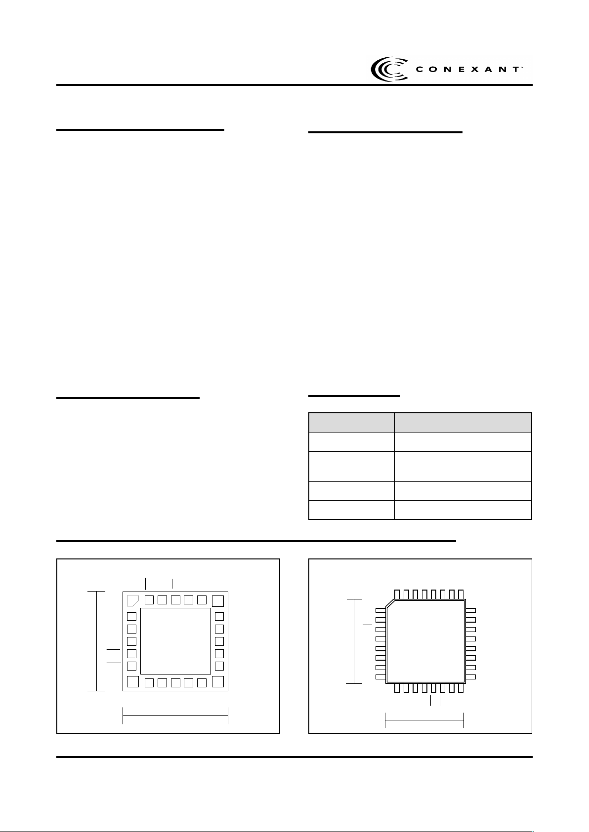
CONNECTIONS
APPLICATIONS ORDERING INFORMATION
CX02066
3.3 Volt Laser Driver IC for Applications to 3 Gbps
PAGE -1-
G High speed operation; suitable for
applications to 3 Gbps.
Typical rise/fall times <90 ps.
G DC or AC coupled modulation drive.
G Differential data and clock inputs to
minimize pattern dependent jitter.
G Independently Programmable Laser Bias
and Modulation currents.
Bias current to 100 mA and modulation current
to 85 mA at VCC=3.3V
G Automatic Laser P ower Control, with
programmable T emperature Compensation
and ‘Slow-Start’.
G Bias and modulation current monitor
G Operates with +3.3 Volt supply
G Functionally compatible with MAX 3869
G The CX02066 is available in die form, or
packages (BCC+24 or TQFP32)
G Short reach SONET/SDH
G Metro SONET/SDH
G Datacomms Modules
CX02066
ADV ANCED INFORMA TION - REV FF
The CX02066 is a highly integrated, programmable
laser driver intended for SONET/SDH applications with
FEC to 3 Gbps. Using differential PECL data and
clock inputs, the CX02066 supplies the bias and
modulation current for driving an edge-emitting laser.
The modulation output can be DC-coupled to the laser
diode, giving a significant power saving over
AC-coupled operation.
The CX02066 includes automatic power control to
maintain a constant average laser output power over
temperature and life. In addition, the modulation
current is temperature compensated to minimize
variation in extinction ratio over temperature.
Output flags indicate laser end of life as well as failure
of the APC circuitry to maintain average output power .
BCC+24 TQFP32TOP VIEW
rebmuNtraP egakcaPniP
PWEID66020XCkcaPelffaW
REFAW66020XC
"01anorefaW"8elohWdednapxE
gniRpirG
42B66020XC42+CCB
23QT66020XC23PFQT
2
3
4
5
6
7
8 9 10 11 12
13
14
15
16
17
18
19
24 23 22 21 20
2066
1
CEN
DIS
GND
TEST
FAIL
OCA
BIAS
OUT+
OUT-
PD
GND
CLK
CLK
V
CC
GND
A
C
MPC
TC
START
TC
SLOPE
MOD
SET
OCA
SET
DIND
IN
V
CC
4mm
4mm
V
CC
DATE CODE
CX02066
1
2
7
6
5
4
3
8
24
23
18
19
20
21
22
17
12
9
10
11
15
141316
29
323130
26
272825
CLK
CLK
CEN
ENA
GND
FAIL
OCA
GND
PD
OUTOUT+
BIAS
V
CC
D
IN
D
IN
V
CC
V
CC
BIAS
MON
MOD
MON
V
CC
V
CC
V
CC
GND
A
GND
A
V
CC
C
MPC
NC
TC
SLOPE
MPC
SET
MOD
SET
OCA
SET
V
CC
5mm
5mm
Page 2
CX02066
3.3 Volt Laser Driver IC for Applications to 3 Gbps
CX02066ADV ANCED INFORMA TION - REV FF
oNniP
42+CCB
emaN noitcnuF
1NEC
,stupniKLCesuotdetcennoCtoNroHGIHteS.)SOMC/LTT(tupnIelbanEkcolC
.stupniKLCgnisutonnehwWOL
2SID .noitarepolamronrofWOL.)SOMC/LTT(elbasiDtuptuOnoitaludoMdnasaiB
51,3DNGdnuorG
4TSETVoteit-niPtseTyrotcaF
CC
5LIAF
onsipoollortnocnehwwolseoG.)SOMC/LTT(rotacidnieruliaFlortnoCrewoPnaeM
.DPtatnerructnatsnocniatniamotelbaregnol
6ACO
InehwwolseoG.)SOMC/LTT(mralAtnerruC-revO
SAIB
saibteserpehtsdeecxe
timiltnerruc
8SAIBtuptuotnerrucsaibresaL
02,7,9V
CC
ylppusrewoP
01+TUODnehwtnerrucskniS.tuptuotnerrucnoitaludomevitisoP
NI
.HGIHsi
11-TUODnehwtnerrucskniS.tuptuotnerrucnoitaludomevitageN
NI
.HGIHsi
21DNG
A
)dnuorgotrotcudni(.egatstuptuorofdnuorG
31DP
rofedonaedoidotohprotinomehtotdetcennocsitupnisihT.tupniedoidotohprotinoM
.lortnocrewopcitamotua
41C
CPM
roticapaceloptnanimodlortnocrewopnaeM
61CT
EPOLS
fotneiciffeocerutarepmetehtstesdnuorgdnanipsihtneewtebrotsiseragnitcennoC
I
TESDOM
.)erutarepmetCIlanretniehtgnisu(
71CT
TRATS
IfotneiciffeocerutarepmetyradnoceS
DOM
ehtstesdnuorgotnipsihtnorotsiserA.
.stratsnoitasnepmocerutarepmetehthcihwtaerutarepmet
81DOM
TES
.tesotdnuorgdnanipsihtneewtebrotsiseratcennoC.testnerrucnoitaludoM
91ACO
TES
.tesotdnuorgdnanipsihtneewtebrotsiseratcennoC.tesmralatnerrucrevO
12D
NI
.desaibfleS.)LCEP(tupnIataDevitisoP
22D
NI
.desaibfleS.)LCEP(tupnIataDevitageN
32KLC .desutonfidetcennocsidevaelnaC.desaibfleS.)LCEP(tupnIkcolCevitisoP
42KLC .desutonfidetcennocsidevaelnaC.desaibfleS.)LCEP(tupnIkcolCevitageN
PIN DESCRIPTION - BCC+24
PAGE -2-
Page 3

CX02066
3.3 Volt Laser Driver IC for Applications to 3 Gbps
CX02066ADV ANCED INFORMA TION - REV FF
PIN DESCRIPTION - TQFP 32
P A GE -3-
oNniP
23PFQT
emaN noitcnuF
1V
CC
ylppuSrewoP
2D
NI
.desaibfleS.)LCEP(tupnIataDevitisoP
3D
NI
.desaibfleS.)LCEP(tupnIataDevitageN
,61,7,4
,12,81
23,52
V
CC
ylppuSrewoP
5KLC .desutonfidetcennocsidevaelnaC.desaibfleS.)LCEP(tupnIkcolCevitisoP
6KLC .desutonfidetcennocsidevaelnaC.desaibfleS.)LCEP(tupnIkcolCevitageN
8NEC
WOL,stupniKLCesuotdetcennoctonroHGIHteS.)SOMC/LTT(tupnIelbanEkcolC
.stupniKLCgnisutonnehw
9ANE .noitarepolamronrofHGIH.)SOMC/LTT(elbanEtuptuOnoitaludomdnasaiB
51,01DNGdnuorG
11SAIB
NOM
rotsiseratcennoC.timiltnerrucsaibtnedneped-erutarepmetdnarotinomsaiB
Vdnanipsihtneewteb
CC
.rotinomot
21DOM
NOM
rotsiseratcennoC.timiltnerrucsaibtnedneped-erutarepmetdnarotinomsaiB
Vdnanipsihtneewteb
CC
.rotinomot
31LIAF
sipoollortnocnehwWOLseoG.)SOMC/LTT(rotacidnieruliaFlortnoCrewoPnaeM
Itatnerructnatsnocniatniamotelbaregnolon
NIP
.
41ACO
InehwWOLseoG.)SOMC/LTT(mralAtnerruC-revO
SAIB
saibteserpehtsdeecxe
timiltnerruc
71SAIBtuptuotnerrucsaibresaL
91+TUODnehwtnerrucskniS.tuptuotnerrucnoitaludomevitisoP
NI
.HGIHsi
02-TUODnehwtnerrucskniS.tuptuotnerrucnoitaludomevitageN
NI
.HGIHsi
Page 4

CX02066
3.3 Volt Laser Driver IC for Applications to 3 Gbps
CX02066ADV ANCED INFORMA TION - REV FF
PIN DESCRIPTION - TQFP 32
P A GE -4-
ABSOLUTE MAXIMUM RATINGS
These are the absolute maximum ratings at or beyond which the IC can be expected to fail or be damaged.
Reliable operation at these extremes for any length of time is not implied.
retemaraP gnitaR stinU
V(ylppusrewoP
CC
)DNG-0.6+ot5.0-V
tneibmagnitarepO 58+ot04-C°
erutarepmeTegarotS 051+ot56-C°
tnerrucsaibresalmumixaM 021Am
)-2TUO/-TUO,+2TUO/+TUOhguorht(tnerrucnoitaudomresalmumixaM 001Am
oNniP
23PFQT
emaN noitcnuF
32,22DNG
A
)dnuorgotrotcudni(egatstuptuorofdnuorG
42DP
rofedonaedoidotohprotinomehtotdetcennocsitupnisihT.tupniedoidotohprotinoM
.lortnocrewopcitamotua
62C
CPM
roticapaceloptnanimodlortnocrewopnaeM
72CN9683XAMhtiwytilibitapmocrofdednuorgebyamdnatcennocoN
82CT
EPOLS
fotneiciffeocerutarepmetehtstesdnuorgdnanipsihtneewtebrotsiseragnitcennoC
I
TESDOM
.)erutarepmetCIlanretniehtgnisu(
92CPM
TES
rewoplacitponaemehtstesdnuorgdnanipsihtneewtebrotsiserA
03DOM
TES
.tesotdnuorgdnanipsihtneewtebrotsiseratcennoC.testnerrucnoitaludoM
13ACO
TES
.tesotdnuorgdnanipsihtneewtebrotsiseratcennoC.tesmralatnerrucrevO
Page 5

CX02066
3.3 Volt Laser Driver IC for Applications to 3 Gbps
CX02066ADV ANCED INFORMA TION - REV FF
AC CHARACTERISTICS
P A GE -5-
(VCC=+3.3V+ 5%, TA=-40°C to +85°C, unless otherwise noted)
RECOMMENDED OPERATING CONDITIONS
retemaraP gnitaR stinU
V(ylppusrewoP
CC
)DNG-3.3+
%01V
)eid(erutarepmeTnoitcnuJ021+ot04-C°
tneibmagnitarepO58+ot04-C°
retemaraP snoitidnoC .niM .pyT .xaM stinU
egatlovtupnilaitnereffiD
D(x2=
NI
+
HGIH
D-NI+
WOL
)
)pihsnoitaleremaswollofstupnikcolc(
003-0681Vm
egnartnerrucnoitaludoM 5.2-58Am
tuptuohtiwtnerrucnoitaludoM
delbasid
HGIH=SID--003
µA
rofegnarelbammargorP
erutarepmettnerrucnoitaludom
tneiciffeoc
elbatsujdA005-01
4
C°/mpp
taerutarepmetelbammargorP
CTtnerrucnoitlaudomhcihw
selbanenoitasnepmoc
RfoeciohcybdemargorP
TESCT
02-06C°
emitesirtuptuonoitaludoM
emitllaftuptuonoitaludoM
252otni%08ot%0 Ω.
252otni%08ot%0 Ω.
--
001
611
sp
tuptuonoitaludomfotoohsrevO
tnerruc
52otnI Ω daol01--01+%
htdiwesluptuptuonoitaludoM
noitrotsid
nrettap0-1gnitanretlagnisuderusaeM--02sp
rettijmodnartuptuonoitaludoMzHM02otzHk21.smr--4IUm
hctaltupniatad(rettijtuptuolatoT
)delbane
52otniderusaeM.kaeP-ot-kaeP Ω daol
2:retliflesseBzHM7681gnisu
32
1-
stupnikcolcgnisu;spbG884.2taSBRP
dnamodnar,DWPsedulcni(
)citsinimreted
--24sp
Page 6

CX02066
3.3 Volt Laser Driver IC for Applications to 3 Gbps
CX02066ADV ANCED INFORMA TION - REV FF
retemaraP snoitidnoC .niM .pyT .xaM stinU
tnerruCylppuS
I
SAIB
IAm05=
DOM
Am05=
DOMIdnaSAIBIgnidulcxE
-75-Am
tnerruCylppuS
I
SAIB
IAm001=
DOM
Am58=
DOMIdnaSAIBIgnidulcxE
-0757Am
egnartsujdatnerrucsaiB
IybdetimiL
FER
erutarepmetssorca
egnar
2- 001Am
tuptuohtiwtnerrucsaiB
delbasid
hgih=elbasiD_xT--003
µA
timiltnerrucsaibmumixaM)elbatsujda(C°58+=AT001
)1(
-- Am
IniegnahC
FER
revo
erutarepmet
elbatsujdA002
)1(
-005
µ C°/A
saibesreveredoidrotinoM
egatlov
2- - V
tnerrucedoidrotinoM
egnartnemtsujda
01- 0051
µA
HGIHtupniSOMC/LTT
)SID,NEC(egatlov
0.2- - V
egatlovWOLtupniSOMC/LTT
)SID,NEC(
-- 8.0V
egatlovHGIHtuptuoSOMC
)ACO,LIAF(
4.2- - V
egatlovWOLtuptuoSOMC
)ACO,LIAF(
-- 4.0V
ecnadepmItupnilaitnereffiDstupnikcolCdnaataD5.2- - kΩ
egatlovtupniedom-nommoCV
CC
83.1--
V
-CC
V
)ffiD(NI
4
V
edomnommocdesaiB-fleS
egatlovtupni
stupnikcolcdnaataDV
CC
83.1--VCC74.0-V
DC CHARACTERISTICS
(VCC=+3.3V+ 5%, TA=-40°C to +85°C, unless otherwise noted)
(1) Default value.
P A GE -6-
Page 7

CX02066
3.3 Volt Laser Driver IC for Applications to 3 Gbps
CX02066ADV ANCED INFORMA TION - REV FF P A GE -7-
FUNCTIONAL DIAGRAM
FUNCTIONAL DESCRIPTION
Overview
The CX02066 laser driver consists of a high-speed
modulation driver and a laser bias generator with mean
power control (MPC). It is optimized for high speed,
low power operation at 3.3V supply. To minimize the
pattern-dependent jitter of the input signal, the device
accepts an input clock signal for data retiming. This
feature can be enabled using the external CEN pin.
Modulator
The modulator output stage is designed to drive up to
85mA in either AC-coupled or DC-coupled mode.
DC-coupled performance depends on the laser used.
The CX02066 modulation output is optimized for
driving a 25Ω load; the minimum required voltage at
OUT+ and OUT- is 0.6V. To interface with the laser
diode, a matching resistor (RD) is required for
impedance matching. An RC shunt network is
necessary to compensate for the laser diode parasitic
inductance, thereby improving the optical eye.
T ypical values are R
SHUNT
= 51Ω, C
SHUNT
= 3.3pF.
These values will need to be optomised for the specfic
laser being used.
Any capacitive loading at the cathode of a laser diode
will degrade the optical output performance. An
inductor is used to isolate the BIAS pin from the laser
cathode.
Mean Power Contr ol
To maintain constant average optical power, the
CX02066 incorporates a control loop to compensate
for the changes in laser threshold current over
temperature and lifetime. A monitor photodiode
mounted in the laser package is used to conv ert the
optical power into a photocurrent. The MPC loop
adjusts the laser bias current so that the voltage at
PD is matched to an on-chip reference voltage . The
external resistor (R
MPCSET
) sets the optical power .
R
MPCSET
= 1.28/I
PIN
I
PIN
is the mean current from the monitor photodiode
at the required mean laser power level (see laster
datasheet).The time constant of the loop is determined
by C
MPC
. In some applications the internal
capacitance on C
MPC
may be sufficient and an
external C
MPC
will not be required.
X100
X60
Fa ilu re
Detect
DIS
ENA
60
30
FAIL
X1
OCA
BIAS
MON
MOD
MON
I
BIAS
I
MOD
OUT-
OUT+
V
CC
I
BIAS
R
MODSET
R
TCSLOPE
R
TCSTART
R
MPCSET
V
CC
C
MPC
V
REF
PD
R
OCA
OCA
SET
RD
GNDA
R
SHUNT
C
SHUNT
CEN
CLK
D
Q
DATA
MPC
SET
NOTE
: BCC+24 Package
PD and MPC
SET
are comm on on P in 13
BIAS
MON
and MO D
MON
are comm on on Pin 14
Page 8

CX02066
3.3 Volt Laser Driver IC for Applications to 3 Gbps
CX02066ADV ANCED INFORMA TION - REV FF
Safety Logic
Safety logic is provided in order to limit the maximum
bias current. The bias current at which the safety
logic trips is set by an external resistor to ground
(R
OCA
) from the OCA
SET
pin. When the bias current
limit is reached alarm flag OCA is asserted LOW . A
loop failure alarm is also provided to detect when the
bias current can no longer be adjusted to achieve the
desired average optical pow er.
Data Input Latch
To minimize input data pattern-dependent jitter, a
differential clock signal can be connected to the data
input latch. If CEN is HIGH, the input data is retimed
by the rising edge of CLK+. If CEN is LO W , the input
data is directly connected to the output stage. If
CEN is left floading it will be pulled HIGH by the internal
circuitry . When this latch function is not used, connect
CLK+ to VCC and leave CLK- unconnected.
Enable Control
The CX02066 incorporates a dual laser driver enable
function. When ENA is LOW or DIS is HIGH, both the
bias and modulation currents are off. Only DIS is
available on the BCC package.
FUNCTIONAL DESCRIPTION
Current Monitors
The CX02066 features bias and modulation current
monitor outputs. The BIASMON output sinks a current
equal to nominally 1/55 of the laser bias current (IBIAS).
The MODMON output sinks a current equal to
nominally 1/55 of the laser peak to peak modulation
current (IMOD). BIASMON and MODMON should be
connected through a pull-up resistor to VCC . Choose
a pull-up resistor value that ensures a voltage at
BIASMON greater than VCC - 1.6V and a v oltage at
MODMON greater than VCC - 1.0V. These pins should
be tied to VCC if not used.
Slow-Start
For laser safety and reliability, the CX02066
incorporates a slow-start circuit that provides a delay
of approximately 200ns before enabling the laser
diode.
P A GE -8-
TYPICAL EYE DIAGRAM
2.5Gbps Optical Eye @ -3dBm
(1.87GHz Filter)
TC
SLOPE
TC
START
80mA
0mA
+80°C-40°C
1
∆
2
∆
R
MPCSET
TEMPERATURE COMPENSATION
Page 9

CX02066
3.3 Volt Laser Driver IC for Applications to 3 Gbps
CX02066ADV ANCED INFORMA TION - REV FF
PACKAGE INFORMATION
Package Outline 24L BCC+
SMT MOUNTING GUIDELINES
BCC Pads
Terminal PCB Land Solder Resist Mask Paste Mask
Corner Pads
Terminal PCB Land Solder Resist Mask Paste Mask
Exposed Central Pad (connected to ground plane)
Terminal PCB Land Solder Resist Mask Paste Mask
Thermal performance <50°C/W
0.4mm
0.3mm
0.35mm
0.1
mm
0.025mm
0.025mm
0.025mm
1.3
mm
0.2mm
0.2mm
0.45mm
0.45mm
1.0mm
1.0mm
0.025mm
0.025mm
0.55mm
0.55mm
0.125mm
0.125mm
2.1mm
2.1mm
1.26mm
1.26mm
0.1mm
0.1mm
0.1mm
0.1mm
0.025mm
0.025mm
0.025mm
0.025mm
0.025mm
0.025mm
P A GE -9-
TOP VIEW BOTTOM VIEW
0.15
Y
X
4
.0
0
±
0
.1
0
4.00±0.10
(PIN 1 CORNER)
"B"
0.50±0.100.50 TYP.
3.15
3.20
"C"
3.20
0.50
±
0.10
0.50 TYP.
3.15
2.20
2.20
C.L(PKG.)
C.L(PKG.)
"A"(PIN 1 CORNER)
Page 10

CX02066
3.3 Volt Laser Driver IC for Applications to 3 Gbps
CX02066ADV ANCED INFORMA TION - REV FF
P A GE -10-
PACKAGE INFORMATION
Package Outline TQFP 32
E1E
D1
D
-B-
-D-
-A-
1
N
TOP VIEW
BOTTOM VIEW
Chamfer .203 (4X)
Exposed Pad
F1
F2
b
A2
A
DETAIL X
DETAIL A
SIDE VIEW
snoisnemiD ecnareloT PFmm00.2+,PFQTmm4.1X5X5 PFmm00.2+,PFQTmm0.1X5X5
NtnuoCdaeL022323
A.XAM06.102.1
1A+
50.050.050.0
2A+
50.004.100.1
3A+
50.05636.05634.0
D+
51.000.700.7
1D+
50.000.500.5
E+
51.000.700.7
1E+
50.000.500.5
L01.0-/51.0+06.006.0
1L.FER00.100.1
e.PYT08.005.005.0
b+
50.053.022.022.0
0*** °7-°0 °7-°0
10+
°4 °6 °6
R.XAM51.051.0
1R.PYT51.051.0
aaa.XAM80.080.0
ccc.XAM80.080.0
1F01.0-/+50.376.2
2F01.0-/+50.376.2
Page 11

CX02066
3.3 Volt Laser Driver IC for Applications to 3 Gbps
CX02066ADV ANCED INFORMA TION - REV FF
BARE DIE INFORMATION
Pad Centres
Chip Layout
* SINGLE PAD/DOUBLE BOND
P A GE -11-
GND V
CC
GNDCLKCLK V
CC
V
CC
GNDV
CC
D
IN
D
IN
BIAS GNDAV
CCA
OUTP OUTN PDGND
A
GND
A
V
CCA
CEN
ENA
DIS
GND
BIAS
MON
MOD
MON
GND
FAIL
OCA
GND
V
CC
V
CC
OCA
SET
MOD
SET
GND
MPC
SET
TC
SLOPE
TC
START
GND
GND
C
MPC
V
CC
Dimensions:
Pad opening 84x84µ
Die Size 1790x1718µ
NIP X Y NIP X Y NIP X Y NIP X Y
NEC727-055SAIB055-117-V
CC
727055-DNG055117
ANE727-044DNG
A
044-117-C
CPM
727044-V
CC
044117
SID727-033V
ACC
033-117-DNG727033-D
NI
033117
DNG727-022PTUO*012-117-CT
EPOLS
727022-D
NI
022117
SAIB
NOM
727-011PTUO*012-117-DNG727011-V
CC
011117
DOM
NOM
727-0 NTUO*001117-CT
TRATS
7270DNG0117
LIAF727-011-NTUO*001117-CPM
TES
727011V
CC
011-117
DNG727-022-V
ACC
022117-DNG727022KLC022-117
ACO727-033-DNG
A
033117-DOM
TES
727033KLC033-117
DNG727-044-DNG
A
044117-ACO
TES
727044V
CC
044-117
V
CC
727-055-DP055117-V
CC
727055DNG055-117
Page 12

Microcosm Sales Offices
Corporate Headquarters
Microcosm Communications Limited
a subsidiary of Conexant Systems, Inc.
Castlemead
Lower Castle Street
Bristol BS1 3AG
United Kingdom
Phone: (44) 117 9302 400
Fax: (44) 117 9302 401
www.mcosm-ic.com
World Wide Direct Sales
Americas
Phone: (503) 590 0540
Fax: (503) 590 3717
Europe, Middle East Africa
Phone: (44) 117 9302 400
Fax: (44) 117 9302 401
Germany
Phone: (49) 6834 609 0000
Fax: (49) 6834 609 0001
Japan
Phone: (81) 48 680 6102
Fax: (81) 48 680 6200
Conexant Sales Offices
Further Information
literature@conexant.com
(800) 854-8099 (North America)
(949) 483-6996 (International)
Network Access
Printed in USA
World Headquarters
Conexant Systems, Inc.
4311 Jamboree Road
Newport Beach, CA
93660-3007
Phone: (949) 483-4600
Fax 1: (949) 483-4078
Fax 2: (949) 483-4391
Americas
U.S. Northwest/
Pacific Northwest - Santa Clara
Phone: (408) 249-9696
Fax: (408) 249-7113
U.S. Southwest - Los Angeles
Phone: (805) 376-0559
Fax: (805) 376-8180
U.S. Southwest - Orange
County
Phone: (949) 483-9119
Fax: (949) 483-9090
U.S. Southwest - San Diego
Phone: (858) 713-3374
Fax: (858) 713-4001
U.S. North Central - Illinois
Phone: (630) 773-3454
Fax: (630) 773-3907
U.S. South Central - T exas
Phone: (972) 733-0723
Fax: (972) 407-0639
U.S. Northeast - Massachusetts
Phone: (978) 367-3200
Fax: (978) 256-6868
U.S. Southeast - North Carolina
Phone: (919) 858-9110
Fax: (919) 858-8669
U.S. Southeast - Florida/
South America
Phone: (727) 799-8406
Fax: (727) 799-8306
U.S. Mid Atlantic Pennsylvania
Phone: (215) 244-6784
Fax: (215) 244-9292
Canada - Ontario
Phone: (613) 271-2358
Fax: (613) 271-2359
Europe
Europe Central - Germany
Phone: +49 89 829-1320
Fax: +49 89 834-2734
Europe North - England
Phone: +44 1344 486444
Fax: +44 1344 486555
Europe - Israel/Greece
Phone: +972 9 9524000
Fax: +972 9 8573732
Europe South - France
Phone: +33 1 41 44 36 51
Fax: +33 1 41 44 36 90
Europe Mediterranean - Italy
Phone: +39 02 93179911
Fax: +39 02 93179913
Europe -Sweden
Phone: +46 (0) 8 5091 4319
Fax: +46 (0) 8 590 041 10
Europe - Finland
Phone: +358 (0) 9 85 666 435
Fax: +358 (0) 9 85 666 220
Asia - Pacific
T aiwan
Phone: (886-2) 2-720-0282
Fax: (886-2) 2-757-6760
Australia
Phone: (61-2) 9869 4088
Fax: (61-2) 9860 4077
China - Central
Phone: 86-21-6361-2515
Fax: 86-21-6361-2516
China - South
Phone: (852) 2 827-0181
Fax: (852) 2 827-6488
China - South (Satellite)
Phone: (86) 755-5182495
China - North
Phone: (86-10) 8529-9777
Fax: (86-10) 8529-9778
India
Phone: (91-11) 692-4789
Fax: (91-11) 692-4712
Korea
Phone: (82-2) 565-2880
Fax: (82-2) 565-1440
Korea (Satellite)
Phone: (82-53) 745-2880
Fax: (82-3) 745-1440
Singapore
Phone: (65) 737 7355
Fax: (65) 737 9077
Japan
Phone: (81-3) 5371 1520
Fax: (81-3) 5371 1501
Advanced Information - REV FF
Page -12CX02066
 Loading...