

Page 1
CORPORATION
Triple 140MHz
CRT Driver
CVA6627S
FEATURES
•• Rise/Fall Ti me. . . . . . . . . . . . . . . . . . . . . . . . . . . . . . . . 3ns
•• Swing . . . . . . . . . . . . . . . . . . . . . . . . . . . . . . . . . . . . 70V
P-P
•• Symmetrical Rise and Fall Time
•• Excellent Gray Scale Linearity
APPLICATION
•• CRT Driver for up to 90khz Monito rs with Resol uti on
upto 1600 x 1280 (Non-Interlaced).
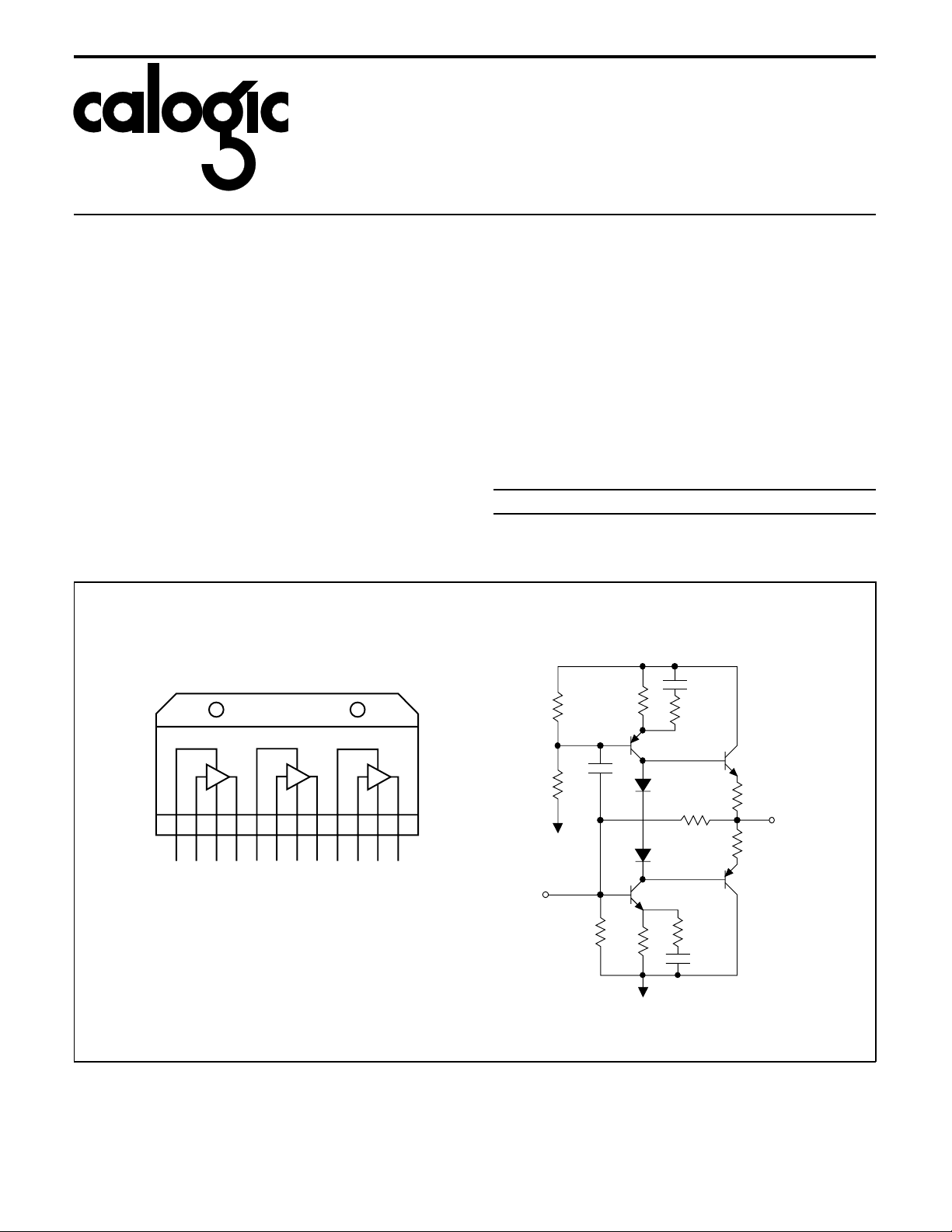
CONNECTION DIAGRAM AND SIM PLIFI ED SCHEM ATIC
DESCRIPTION
The CVA6627S contains three wideband amplifiers designed
specifically to drive high resolution CRTs . It features excellent
gray scale linearity and high load capacitance driving
capability. This device can drive monitors with resolution of
1600 x 1280 (non-interlac ed) with pixel freque ncy of 300 MHz.
The part is housed in 12L Ceramic package with heat sink
grounded.
ORDERING INFORMATION
Part Package Temperature
o
CVA6627S CY12B -20
Q1
C to +100oC
Q2
5.7K
1
3
1
2
4
5
6
7
8
9
IN R
V+ R
GND R
IN G
V+ G
OUT R
OUT G
GND G
V+ B
12
11
10
IN B
OUT B
GND B
250
Q3
Q4
1j-40
CALOGIC CORPORA TION, 237 Whitney Place, Fremont, California 94539, Telephone: 510-656-2900, FAX: 510-651-30 25
Page 2
CVA6627S
ABSOLUTE MAXIMUM RATINGS
Supply Voltage. . . . . . . . . . . . . . . . . . . . . . . . . . . . . . . . . . 85V
Storage Tempera tu re. . . . . . . . . . . . . . . . . . -2 5
o
C to +125oC
CORPORATION
Operating Temperature . . . . . . . . . . . . . . . . - 20
o
C to +100oC
Lead Temperat ure . . . . . . . . . . . . . . . . . . . . . . . . . . . +300
o
C
DC ELECTRICAL CHARACTERISTICS VS = 80V, CL = 10pF , V
SYMBOL CHARACTERISTICS MIN TYP MAX UNITS
I
CC
V
IN DC
V
OUT DC
A
V
Supply Current 26 32 mA
Input DC Level 1.4 1.6 1.8 V
Output DC Level 34 38 42 V
Voltage Ga in 11 13 15 V
Gain Matching 0.2 dB
AC ELECTRICAL CHARACTERISTICS VS = 80V, CL = 10pF , V
SYMBOL CHARACTERISTICS MIN TYP MAX UNITS
t
r
t
f
BW Bandwidth 140 MHz
Le Linearity 5 %
OS Overshoot 4 %
Rise Time 3.1 4.0 ns
Fall Time 3.1 4.0 ns
OUT
OUT
= 50V
= 50V
P-P
P-P
, T
= +25oC. See Figure 1.
CASE
, T
= +25oC. See Figure 1.
CASE
FIGURE 1. TEST CIRCUIT
V
CC
C4 C6
L1
OUTPUT
C
L
INPUT
C1
C2
R1
R2
C3
2,6,10
V
R4
1/3
CVA6627S
IN
1,5,9
V
CC
4,8,12
V
OUT
D1
R5 R6
D2
3,7,11
GND
R1 = 15Ω
R2 = 430
R4 = 200k
Ω
R5 = 22Ω
R6 = 22Ω
C1 = VARIABLE 20 TO 150pF
TYPICAL 68pF
C2 = VARIABLE 4 to 20pF
TYPICAL 17pF
C3 = 75pF
C4 = 10µf/160V
C6 = 0.01 µf/160V
C = 10pF
L
D1 = DS464
D2 = DS464
L1 = 150nH
1J-32
CALOGIC CORPORAT ION, 237 W hit ney Place , Fremo nt, Califor nia 94539, Telephone: 510-656-2900, FAX: 510-651-3025
Page 3

CORPORATION
APPLICATION INFORMATION
CVA6627S
The CVA6627S is a transimpedance amplifier with two stage
feedback configurations. Any change in input current will be
reflected as change in output voltage swing. A resistor in
series with the input will change the CVA6627S into a voltage
amplifier. The output is emitter follower with load(capacitive)
driven capability.
With a true Class AB output stage, the rise and fall time is
symmetric.
CVA6627S has an internal feedback resistor of 5.7KΩ. In the
absence of any input signal, the V
R
V
OUT
(DC) = (1 +
F
) VIN (DC); RB = 250Ω.
R
B
DC is set by
OUT
An input resist or RG will set the gain as
R
F
= (
V
OUT
) VIN ; RG = gain resistor.
R
G
Input and Transfer Cha racteristics
An input current swing of ±4. 4mA causes the output to c hang e
by ±25V. A resistor of 430Ω will set the gain to -13. Input pins
are internal DC feedback nodes and thus have low
impedance. These pins must be fed fro m a series RC net wor k
for high frequenc y empha sis.
The following section will explain how to overcome some of
the problems that are typical.
1) Input drive: CVA6627S gives best results when the
amplifier is driven by a fast pulse with proper voltage level.
Since all pre-amplifiers have output from 0 to 8V, a level
shifter is required. Also, most pre-amplifiers cannot drive a
large capacit ive load.
2) Smear: For a box pattern with white background, a shadow
after the black is cal led smear. It is due to the tilt of the white
level. It can easily be adjusted by adding an RC feedback
network (R4, C3). The value of R4 will affect the gain, for
CV A6627 S, the typical value is 200K.
3) Streaks and overshoot: For a cross-hatch pattern with
white background, a whitish line will appear just after the
black line, this is called s treak. Looking at the waveform it is
due to undershoot of the waveform. For a Box pattern with
white background, a dark black area just after white is a sign
of overshoot. It is due to overshoot of the wavef or m. Adju stin g
the value of C2, R1, C1 will get the optimum result. The value
of C2 should be kept at minimum for less overshoot, typical is
<20pF. Value of R1 should be less than 47 ohms otherwise
rise and fall time will suffer. First adjust the overshoot to
minimum, keeping value of C1 and R2 to minimum, then
adjust the undershoot (Streak) by adjusting C3 again. Since
both need to be adjusted together, this may need a few
iteration to get to the opt im um r esult .
It should be n oted here that the output peaking with L1 and
R3 is only to overcome the affect of stray capacitance. Keep
the value of L1 to minimum, typ 150nH and R, to be 820Ω.
The value of L1 depends on the associated capacitance with
the board and the cable(if any). CVA6627S is specifically
designed to handle extra capacitance associated with the
cable(typ. 10pF) assuming the driver is not part of the neck
board. The value of R3 should be less than 1K to damped the
resonant ring in g.
The output of CVA6627S is not short circuit proof. Precaution
is required.
Thermal Characteristics
Under normal operating conditions the CVA6627S will
dissipate up to 11W . The maximum allowed case tem p er atur e
is +100
o
C. To calculate maximum heatsink thermal resistance
use the following equation:
(100 − 50°)
Rth =
11W
= 4.5°C/W
The Thermalloy #11699 is one example of a heatsink that
meets this requir emen t.
CALOGIC CORPORA TION, 237 Whit ney Place, Fremont , Ca lifor nia 94539, Telephone: 510-656-2900, FAX: 510-651-3025
Page 4

CVA6627S
1J-34
P-P
BOX PATTERN — 50V
20ns/DIV
10V/DIV
1J-36
CROSS HATCH PATTERN
— WHITE BACKGROUND
10ns/DIV
10V/DIV
FIGURE 2. APLICATION CIRCUI T
12V
CORPORATION
.01µF
PRE
AMP
R6
10pF
.01µF
–5V
R1 = 15Ω
R2 = 430 Ω
R3 = 820
ELECTRICAL CHARACTERISTICS
BOX PATTERN — 50V
10V/DIV
10pF
Q1
D1
V = –0.5V
MIN
R4 = 200K
R5 = 39Ω
R6 = 120 Ω
Ω
R1
R3
C2
C1
D1 = DS464
D2 = DS464
L1 = 150nH
CVA6627S
R4
1,5,9
3,7,11
C3
2,6,10
C1 = VARIABLE 20 TO 150pF
TYPICAL 68pF
C2 = VARIABLE 4 to 20pF
TYPICAL 17pF
4,8,12
C4
DC RESTORE
C3 = 75pF
C4 = 1µF
D2
L1
R5
CRT
R3
D3
1J-37
P-P
20ns/DIV
1J-33
CROSS HATCH PATTERN
— BLACK BACKGROUND
10V/DIV
10ns/DIV
1J-35
CALOGIC CORPOR ATION, 237 Whitney Place, Fremont, California 94539, Telephone: 510-6 56-290 0, FAX: 510-651-3025
 Loading...