

Page 1
CORPORATION
185MHz CRT Driver
CV A3424 A / CVA3 424
FEATURES
Bandwi dt h . . . . . . . . . . . . . . . . . . . . . . . . . . . . . . 185MHz
••
Rise/Fall Ti me. . . . . . . . . . . . . . . . . . . . . . . . . . . . . . 2.5 ns
••
Swing . . . . . . . . . . . . . . . . . . . . . . . . . . . . . . . . . . . 40V
••
Supply Voltage. . . . . . . . . . . . . . . . . . . . . . . . . . . . . . . 80V
••
APPLICATIONS
CRT Driver for 2000 x 1600, 1600 x 1280 and 1280 x 1024
••
Monitors
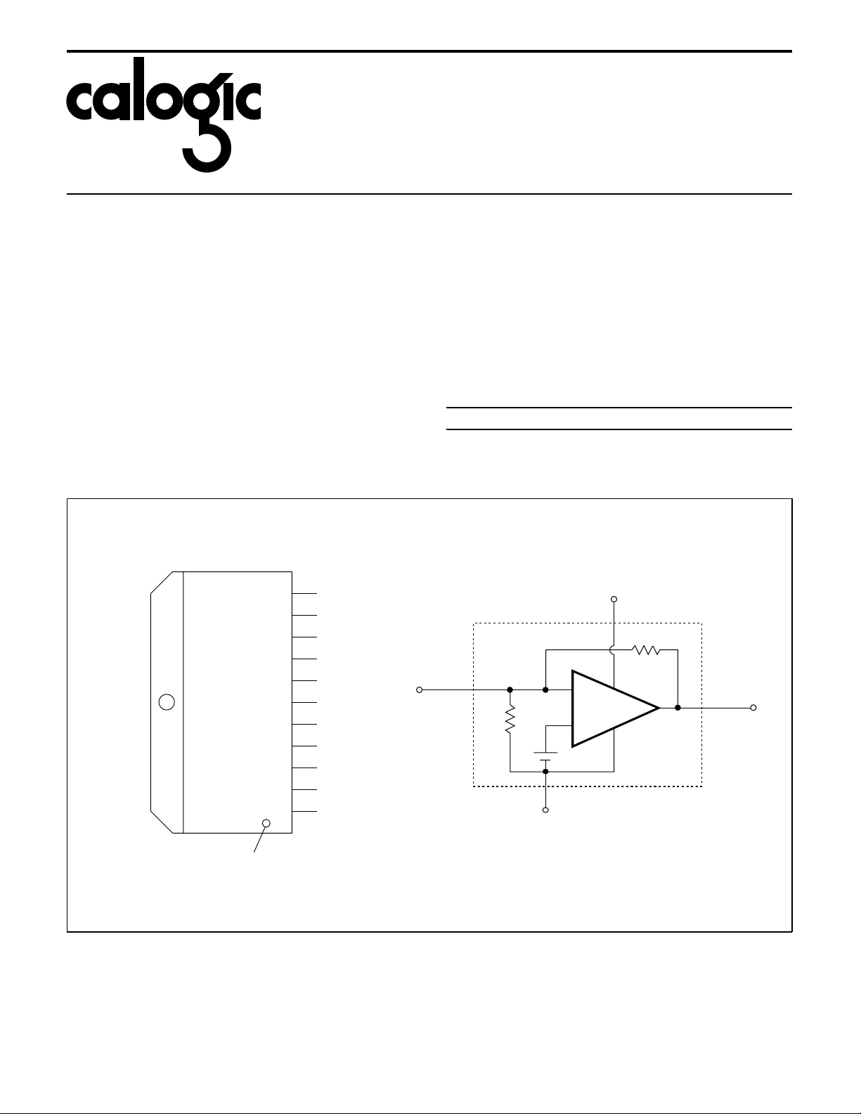
CONNECTION DIAGRAM AND SIM PLIFI ED SCHEM ATIC
11
V
cc
10
NC
9
V
out
8
GND
7
GND
6
GND
5
NC
4
NC
3
V
in
2
NC
1
NC
P-P
DESCRIPTION
The CVA3424 Family is a video driver amplifier designed
specially to drive high resolution color monit ors. With rise and
fall time of under 2.5ns and 185MHz bandwidth, this device
will provide excellent drive capability for the 2000 x 1600,
1600 x 1280 and 1280 x 1024 monitors.
ORDERING INFORMATION
Part Package Temperature
o
CVA3424AT TO-220 -20
CVA3424T TO-220 -20
V
CC
11
3.66kΩ
V
in
3
142Ω
R
B
GND
6,7,8
CVA3424
R
F
C to +90oC
o
C to +90oC
V
out
9
1B-04
PIN 1 DESIGNATOR
T11A
1C-04
Page 2
CVA3424A / CV A3424
ABSOLUTE MAXIMUM RATINGS
Supply Voltage. . . . . . . . . . . . . . . . . . . . . . . . . . . . . . . . . . 85V
Storage Tempera tu re. . . . . . . . . . . . . . . . . . -25
o
C to +100oC
CORPORATION
Operating Tempera tu re . . . . . . . . . . . . . . . . . -20
o
C to +90oC
Lead Temperature . . . . . . . . . . . . . . . . . . . . . . . . . . . +300
o
C
DC ELECTRICAL CHARACTERISTICS VS = 80V, CL = 10pF , V
SYMBOL CHARACTERISTICS MIN TYP MAX UNITS
I
CC
V
V
A
inDC
outDC
V
Supply Current 45 55 mA
Iput DC Level 1.4 1.6 1.8 V
Output DC Level 34 40 46 V
Voltage Ga in 11 13 15 V
Gain Matching 0.2 dB
AC ELECTRICAL CHARACTERISTICS VS = 80V, CL = 10pF , V
SYMBOL CHARACTERISTICS
t
r
t
f
BW Bandwidth 185 150 MHz
Le Linearity 5 5 %
OS / US Overshoot / Undershoot 8 8 %
Rise Time 2.2 2.9 2.5 3.5 ns
Fall Time 2.5 2.9 2.7 3.5 ns
MIN TYP MAX MIN TYP MAX
CVA3424A CVA3424
out
out =
= 40V
40V
. See Figure 1. TA = +125oC unless otherwise note d.
p-p
. See Figure 1. TA = +125oC unless otherwise noted.
p-p
UNITS
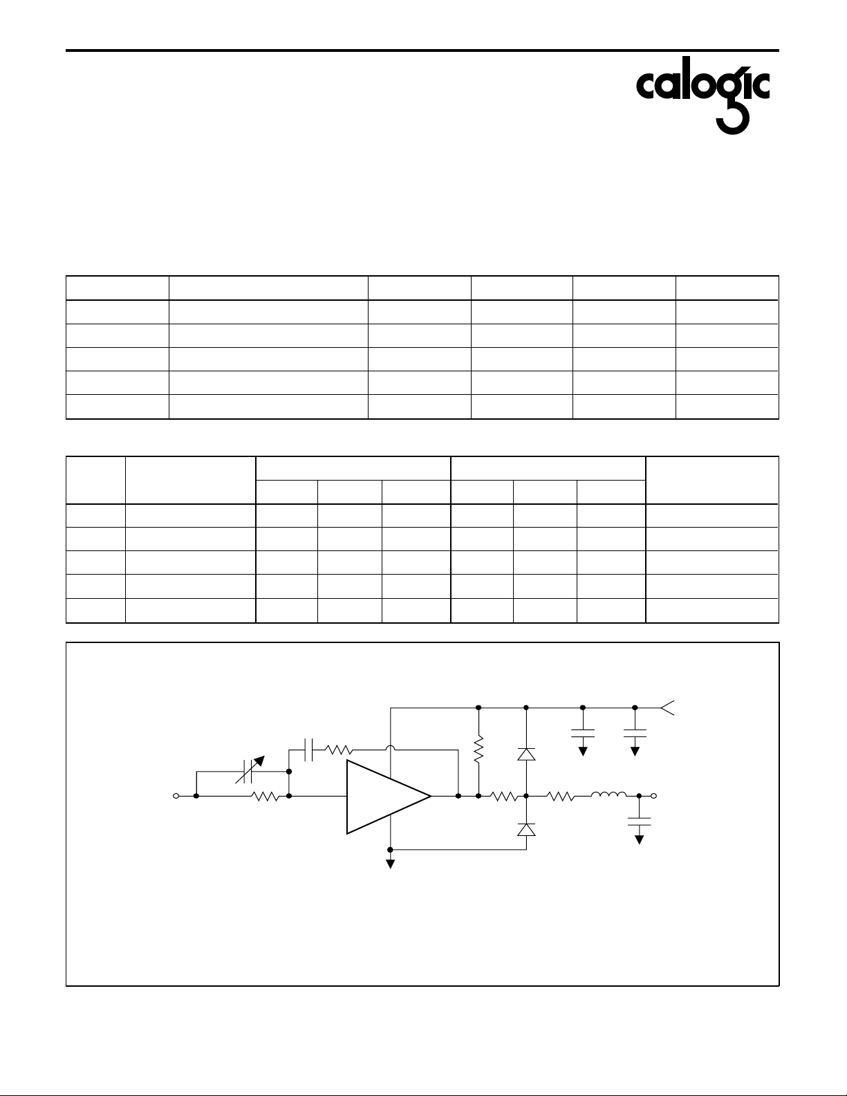
FIGURE 1. TEST CIRCUIT
INPUT
C2
R1 = 270 Ω
R2 = 12kΩ (1 W)
R4 = 300k Ω
R5 = 15Ω
R6 = 15Ω
C3
R1
R4
39
V
in
C2 = Variable 4 to 150pF
Typical 27pF
C3 = 46pF
C4 = 10µf/160V
11
CVA3424
6,7,8
GND
V
CC
C4 C6
R2
V
CC
V
out
D1
R5 R6
L1
D2
C6 = 0.01µf/160V
C = 10pF (Including
L
Parasitics)
D1 = DS464
D2 = DS464
L1 = 150nH
1
OUTPUT
C
L
1B-05
Page 3

CORPORATION
BANDWIDTH
100
MHz
110
GAIN
5dB/DIV
0dB
APPLICATIONS INFORMATION
CV A3424 A / CVA3 424
Basic Circui t Con figu rat io n
The CVA3424 is a transimpedance amplifier with two stage
feedback amplifier configurations. Any change in input
current will be reflected as change in output voltage swing. A
resistor in series with the input will change the CVA3424 into
a voltage amplifier. The output is an emitter follower.
Because of the compl ementary circuitry employed, there is
no need for load or pull up resistor.
An internally bypassed capacitor is included inside the
package, however, for low frequencies an electrolytic
capacitor is recommended.
CVA3424 has an internal feedback resistor of 3.66KΩ. In the
absence of any input signal, the V
R
(DC) = (1 +
V
out
F
) Vin (DC)
R
B
DC is set by
out
If an input signal is applied, the gain is set by
R
F
= (
V
out
) V
in
R
x
Input and Transfer Characteristics
An input current swing of ±4. 5mA causes the output to c hang e
by ±25V.
A resistor of 270Ω in series with the input will give a voltage
gain of -13.
Input pins are internal dc feedback nodes and thus have low
impedances. These pins must be fed from a series RC
network for high fre quen cy emph asis.
Output Char act er i st ic s
The CVA3424 is in tended to be used as th e final stage of very
fast video circuits. The nominal load capacitance is 10pF. Other
values can be accommodated since the output stage is an
emitter follower and is fairly insensitive to load capacitance.
However, a wire connection of som e length is unavoidable, t hat
causes objectionable ringing due to a r esonant circuit. To avoid
this a damping resistor must be used in series with the lead
inductance . A lso a resistor is necessary to protect the ampli fier
against arching. A resistor of 30-50Ω will provide protection but
will slow down the response. The lead inductance may be
artificially increased by a tenth of a microHenry to obtain
desired peak. Any change in inductance will require
readjustment of damping r esistor, as stated by equation (1).
L
∗
= √
C
(1)
R
The output of CVA3424 is not short circuit proof. Any
resistance to V+ or Ground shou ld be >600 Ω.
Thermal Characteristics
When low frequency square waves are amplified, some droo p
wil l occur due to a la rge change in the rmal dissipation in the
input transistors. To overcome this an R-C series feedback
network is suggested with 300kΩ and 46pF values. Under
normal operating conditions the CVA3424 will dissipate up to
6W. The maximum allowed case temperature is +90
o
C. To
calculate maximum heatsink thermal resistance use equation (2).
(
90 − 50°)
Rth
=
= 6.7°C/W
6W
8V/DIV
VOLTS
FALL TIME
2ns/DIV
8V/DIV
VOLTS
RISE TIME
2ns/DIV
Page 4

CORPORATION
CVA3424
Inform at ion furni shed by Calogic is believed to be accurate and reliable. Howe ver, no responsibility is assum ed for its use: nor for any in fring eme nt of pate nts or other
rights of third parties which may result from its use. No license is granted by implication or otherwise under any patent rights of Calogic.
CALOGIC CORPORATION, 237 Whitney Plac e, Fremont, C alifornia 94 53 9, Telephon e: 510-656-2 900, F AX: 510-651 -1076
 Loading...