

Page 1
CORPORATION
1P-13
9
V
CC
1,3,5
V
BIAS
V
OUT
11,9,8
V
IN
R
1
R
4
R
5
R
2
10
R
3
R
6
R
1
TAB = GND
2,4,7
Low Cost
Triple CRT Driver
CVA2405T
FEATURES
•• Rise/Fall Ti me. . . . . . . . . . . . . . . . . . . . . . . . . . . . . . . 4.0ns
•• Swing . . . . . . . . . . . . . . . . . . . . . . . . . . . . . . . . . . . 65V
•• Supply Voltage. . . . . . . . . . . . . . . . . . . . . . . . . . . . . . . 90V
•• Excellent Gray Scale Linearity
•• Consist ent EMI Perform a nce
APPLICATIONS
•• CRT driver for up to 69kHz monitor s with resolutio n up
to 12 80 x 1 02 4.
•• Excellent Gray Scale Linearity
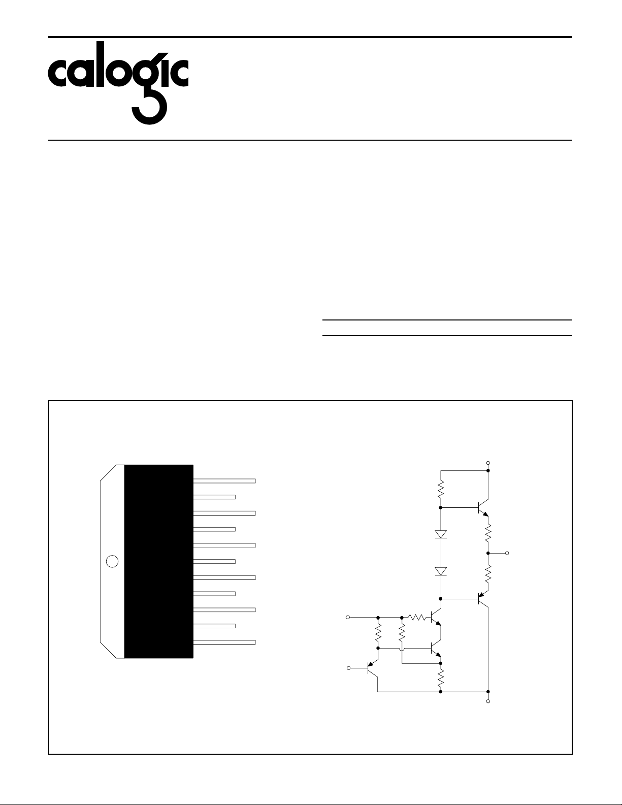
CONNECTION DIAGRAM AND SIM PLIFI ED SCHEM ATIC
11
10
9
8
7
6
5
4
3
2
1
GND = TAB
V
BIAS
V
IN
V
CC
GND
GND
TOP VIEW
T11A PACKAGE
V
V
3
V
V
IN
IN
GND
OUT
V
OUT
OUT
DESCRIPTION
The CVA2405T contains three high impedance wideband
P-P
amplifiers, de signed speci fically to drive a CRT. It features no
crossover distortion for excellent gray scale linearity. This device
can drive monitors with resolutions of 1280 x 1024
(non-interlaced) with pixel frequency of 160MHz.
The part is housed in the industry standard 11-lead TO-220
molded power pack age. The heat sink is gr ounded.
ORDERING INFORMATION
Part Package Temperature
o
CVA2405T T11A -20
1
2
3
2
1
1P-12
C to +100oC
CALOGIC CORPOR ATION, 237 Whitney Place, Fremont, California 94539, Telephone: 510-6 56-290 0, FAX: 510-651-3025
Page 2
CVA2405T
GND
TAB
1P-14
V
IN
V
BIAS
C1 = 0.01µF
C2 = 100
µ
F
C3 = 0.1
µ
F
D1, D2 = FHD400
C4 = 100
µ
F
C6 = 8pF
C6
C4C3
C2C1
D2
D1
VIDEO
INPUT
V
CC
11,9,8
10
1,3,5
V
OUT
2,4,7
TEKTRONIX
FET PROBE
MODEL 620 1
(CAP. 1.5pF)
CVA2405T
6
ABSOLUTE MAXIMUM RATINGS
Supply Voltage. . . . . . . . . . . . . . . . . . . . . . . . . . . . . . . . . . 90V
Power Dissipation . . . . . . . . . . . . . . . . . . . . . . . . . . . . . . . 16W
Storage Tempera tu re. . . . . . . . . . . . . . . . . . . -50
o
C to +150oC
CORPORATION
ESD . . . . . . . . . . . . . . . . . . . . . . . . . . . . . . . . . . . . . . . . 2000V
Operating Temperature . . . . . . . . . . . . . . . . . -20
Lead Temperat ure . . . . . . . . . . . . . . . . . . . . . . . . . . . . +300
o
C to +100oC
o
C
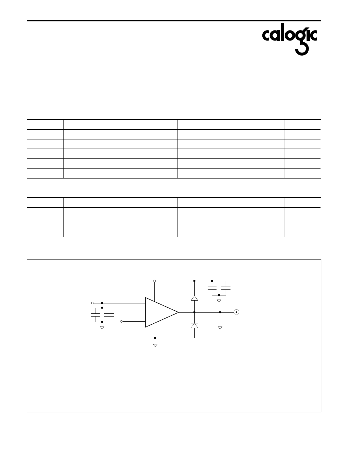
DC ELECTRICAL CHARACTERISTICS Vs = 80V, CL = 8pF, DC
INPUT BIAS
= 12V, VIN = 2.6V, V
OUT
= 50V
p-p
. T
CASE
See Figure 1.
SYMBOL CHARACTERISTICS MIN TYP MAX UNITS
I
cc
I
B
V
OUT DC
A
v
AC ELECTRICAL CHARACTERISTICS Vs = 80V, CL = 8pF, DC
Supply Current, Per Chann el 20 30 mA
Bias Current 40 mA
Output DC Level 47 50 53 V
Voltage Gain -11 -13 -15 V
Gain Matc h ing 0.5 dB
INPUT BIAS
= 12V, VIN = 2.6V, V
OUT
= 40V
p-p
. T
CASE
See Figure 1.
SYMBOL CHARACTERISTICS MIN TYP MAX UNITS
T
r
T
f
L
e
Rise Time 6 ns
Fall Time 6ns
Linearity 5%
FIGURE 1. TEST CIRCUIT
= +25oC.
= +25oC.
CALOGIC CORPOR ATION, 237 Whitney Place, Fremont, California 94539, Telephone: 510-6 56-290 0, FAX: 510-651-3025
Page 3

CORPORATION
1P-15
V
BIAS
VIDEO
CVA2405T
+80V
L
R
91
Ω
SPARK
GAP
33
Ω
FIGURE 2.
FIGURE 3.
CVA2405T
+80V
V
BIAS
VIDEO
CVA2405T
1K
APPLICATION INFORMATION
The CVA2405T is a high voltage triple CRT driver suitiable to
drive 69kHz, 1280 x 1024 CRT displays. It features a high
impedance input to match any pre-amplifier. The CVA2405T
has a true class AB output stage that results in excellent gray
scale linearity and consisten t EMI per for mance .
As with any high speed amplifier used in CRT display
applications, specific precaution should be taken to get the
required performance. Power supply should be by pass as
close to the device pin as possible. Use 0.01µf very near to
the device and a large capacitor of 10µf or more (preferable
100µf) near the device. A 0.1µf and 10µf should be connected
near the V
pin (#10). Arc protection is very essen tial. Fast
bias
diodes together with the spark gap will achieve sufficient
protection. However, in certain applications depends on the
tubes a high value of resistor is required to reduce the cur rent
into the CVA2405T during arcing. This will result in less than
desireable performance some of which can be restored by
using a peaking inductor at the output pin,
Figure 2
. Another
way to achieve this is by using a RC network at the output of
the device and use a peak ing in duct or at the tube,
The rise and fall time of the CVA2405T may suffer due to
stray capacitances associated with the PC Board and other
components. It can be improved by carefully designing the
PC Board where the output stage and input stage ground path
are seperated. Calogic will assist customers in the layout of
Figure 3
L
R
C
CVA4501
DC BIAS
I.C.
BIAS
33
Ω
V
cc
SPARK
GAP
1P-16
the PC Board that will result in quick EMI passage and better
performance. The output peaking should be used only to
restore the performance loss due to stray capacitances. O ver
peaking will cause excessive ringing that will have better
results but poor EMI. The DC restore circuit is also important
when considering the high frequency performance. Using
CVA4501, DC Bias IC, better results can be obtained and
high frequency pe rfor ma n ce can be maximixed.
THERMAL CONSIDERATIONS
Power supply current increases as the input signal increases
and consequen tly po wer dissipat ion also incr ea ses.
The CVA2405T cann ot be used withou t heat sinking.
Figure 4
shows the power dissipated in each channel over the
operating voltage range of the device. Under white screen
conditions, i.e.: 25V output, dissipation increases to 10.8W
total. The CVA2405T case temperature must be maintained
below +100
temperatur e is + 5 0
o
C. If the maximum expected ambient
o
C, then a heat sink is needed wit h ther m a l
resistance equa l to or less than:
10.8W
o
C)
= 4.6oC/W
+
.
.
R
=
th
(100 − 50
The CV A 24 05T maximum load is 600 Ω to ground or V
The output of CV A2405T i s not shor t ci rc uit pr oof . Any r e sist ance
+
or Ground should be > 600Ω.
to V
CALOGIC CORPOR ATION, 237 Whitney Place, Fremont, California 94539, Telephone: 510-6 56-290 0, FAX: 510-651-3025
Page 4

CVA2405T
16
14
12
10
8
6
4
2
0
1P-19
POWER DISSIPATION vs V
POWER (W)
(V)V
CC
55
60 65 70 75 80 85
= 25V
V
OUT
= V = 10V
V
OUT CC
CC
1P-21
PULSE RESPONSE
VOLTS (V) 10V/DIV.
TIME = 20ns/DIV.
FIGURE 4. APPLICATION CIRCUI T
V
BIAS
R2
C2C1
VIDEO
INPUT
V 6
CC
10
V
11,9,8
CVA2405T
IN
GND
TAB
2,4,6
V
OUT
1,3,5
D1
D2
C5
DC BIAS
R1
CORPORATION
C4C3
L
R3
SPARK
GAP
TYPICAL CHARACTERISTIC S
V vs V
1234567
(V)V
OUT
80
70
60
50
40
30
20
10
0
0
0
R1 = 820
R2 = 22
R3 = 47(1/2W)
OUT IN
(V)
V
IN
BANDWIDTH
Ω
1P-18
C1 = 0.01µF
µ
C2 = 100
C3 = 0.1
C4 = 100
C5 = 2.2
F
µ
F
µ
F
µ
F
C7 = 40 - 120pf
D1, D2 = FHD400
L = 150 - 33nH
1P-17
Ω
Ω
5
10
15
5 dB / DIV.
20
25
30
1MHz
10MHz 100MHz
1P-20
CALOGIC CORPOR ATION, 237 Whitney Place, Fremont, California 94539, Telephone: 510-6 56-290 0, FAX: 510-651-3025
 Loading...