

Page 1
CRD4202-1
CrystalClear™ AC '97 Six Channel CNR Audio Reference Design
Features
! Six Channel Analog Audio Outputs
! Headphone Sense using GPIO
! CS4202 codec and two CS4334 DACs
! 20-bit D to A conversion (DAC)
! 18-bit A to D conversion (ADC)
! S/PDIF (IEC-958) optical digital output
! Complete suite of Analog I/O connections:
– Line, Mic, CD, Video, Modem, and Aux Inputs
– Modem, Headphone, Line Front, Line Rear
and Line C enter/Sub-Woofer Outputs
! 2-layer low cost PC board
! Meets Intel
! Exceeds Microsoft’s
performance requirements.
®
AC '97 revision 2.2
®
PC 2001 audio
Description
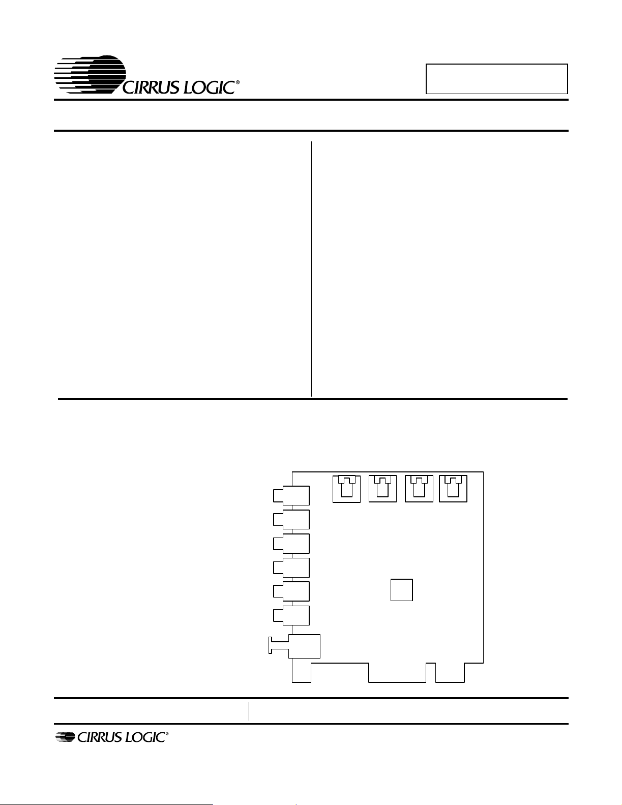
The CRD4202-1 reference design features six channel
analog audio outputs, an optical S/PDIF digital output,
and Communication and Networking Riser (CNR) interface. This design uses the CS4202 audio codec which
has several advanced features including a built-in headphone amplifier, simultaneous six channel analog and
S/PDIF optical digital output, GPIO for headphone detection, and up to 30 dB of internal microphone boost.
The CRD4202-1 reference design is available by ordering the CMK4202-1 manufacturing kit. This kit includes
the CRD4202-1 board, a full set of schematic design
files (OrCAD
PCB artwork files, and bill of materials. This reference
design offers significant cost savings over competing
solutions and can be easily modified to meet your specific design goals.
ORDERING INFO
CMK4202-1 (Manufacturing Kit)
®
format), PCB job files (PADS®ASCII),
Microphone Input
Line Input
Line Output
Headphone Output
Rear Channel Output
Center / Sub-Woofer Output
S/PDIF Digital Optical Output
Preliminary Product Information
P.O. Box 17847, Austin, Texas 78760
(512) 445 7222 FAX: (512) 445 7581
http://www.cirrus.com
MIC
IN
LINE
IN
LINE
OUT
HEADPH
OUT
SURR
OUT
CNT/LFE
OUT
S/PDIF
OUT
This document contains information for a new product.
Cirrus Logic reserves the right to modify this product without notice.
Copyright Cirrus Logic, Inc. 2002
(All Rights Reserved)
CS4202
AUX INVIDEO INCD ININT MODEM
Cirrus Logic
CRD4202-1
DS549RD1A1
JAN ‘02
1
Page 2

TABLE OF CONTENTS
1. GENERAL INFORMATION ...................................................................................3
2. SCHEMATIC DESCRIPTION ................................................................................3
2.1 CS4202 Audio Codec .................................................................................3
2.2 Analog Inputs ..............................................................................................3
2.3 Rear Channel and Surround Outputs .........................................................4
2.4 Front Channel and Headphone Outputs .....................................................4
2.5 S/PDIF Optical Output ................................................................................4
2.6 CNR Connector and EEPROM ...................................................................4
2.7 Auto Demotion Circuit .................................................................................4
2.8 Phase Locked Loop (Optional) ...................................................................4
2.9 Component Selection .................................................................................4
2.10 EMI Components ......................................................................................5
3. GROUNDING AND LAYOUT ................................................................................5
3.1 Partitioned Voltage and Ground Planes .....................................................5
3.2 AC-Link .......................................................................................................5
3.3 CS4202 Layout Notes .................................................................................5
4. REFERENCES .......................................................................................................6
4.1 ADDENDUM ...............................................................................................6
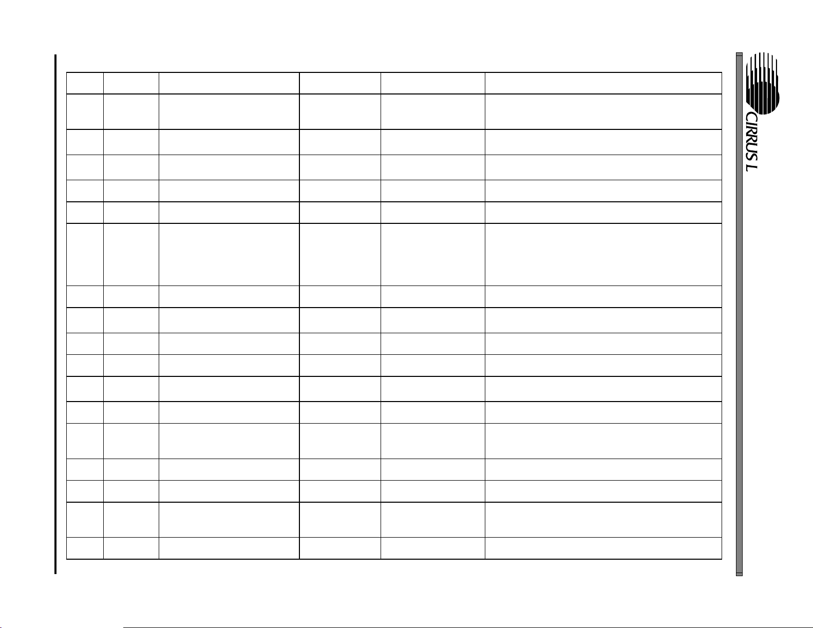
5. BILL OF MATERIALS .........................................................................................21
CRD4202-1
LIST OF FIGURES
Figure 1. Block Diagram ....................................................................................................7
Figure 2. CS4202 Audio Codec .........................................................................................8
Figure 3. Analog Inputs ......................................................................................................9
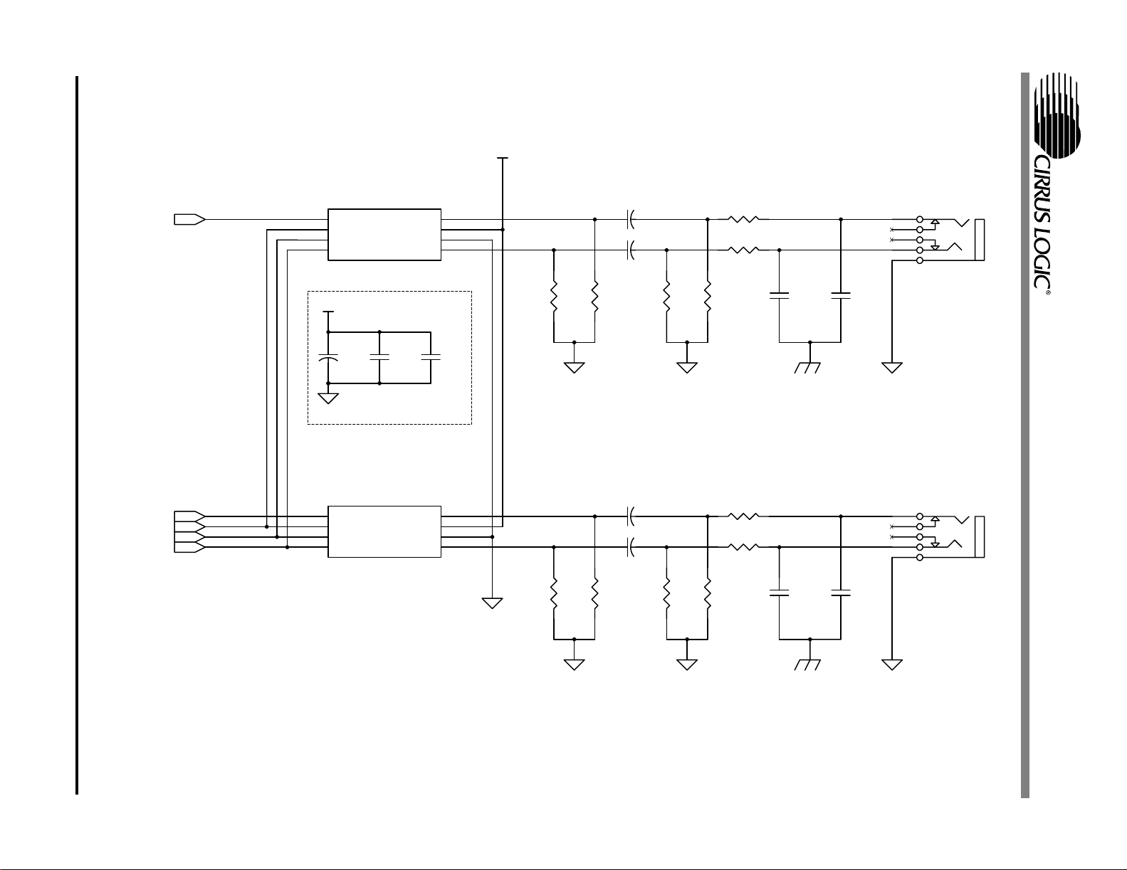
Figure 4. Center Channel, Surround, and Sub-Woofer Outputs ......................................10
Figure 5. Front Channel and Headphone Sense Output .................................................11
Figure 6. S/PDIF Optical Output ......................................................................................12
Figure 7. CNR Connector ................................................................................................13
Figure 8. Phase Locked Loop ..........................................................................................14
Figure 9. Auto Demotion and Serial Buffers ....................................................................15
Figure 10. PCB Layout: Top Assembly Drawing ..............................................................16
Figure 11. PCB Layout: Top Layer ..................................................................................17
Figure 12. PCB Layout: Bottom Layer .............................................................................18
Figure 13. PCB Layout: Drill Drawing ..............................................................................19
Figure 14. PCB Layout: Top Silkscreen ...........................................................................20
Contacting Cirrus Logic Support
For a complete listing of Direct Sales, Distributor, and Sales Representative contacts, visit the Cirrus Logic web site at:
http://www.cirrus.com/corporate/contacts/
Microsoft, Windows 95, Windows 98 and Windows Millennium and WHQL is registered trademark of Microsoft.
CrystalClear is a trademark of Cirrus Logic, Inc.
Intel is a registered trademark of Intel Corporation.
OrCAD is a registered trademark of OrCAD, Inc.
PADS is a registered trademark of, PADS Software, Inc.
Preliminary product information describes products which are in production, but for which full characterization data is not yet available. Advance product information
describes products which are in development and subject to development changes. Cirrus Logic, Inc. has made best efforts to ensure that the information contained
in this document is accurate and reliable. However, the information is subject to change without notice and is provided “AS IS” without warranty of any kind (express
or implied). No responsibility is assumed by Cirrus Logic, Inc. for the use of this information, nor for infringements of patents or other rights of third parties. This
document is the property of Cirrus Logic, Inc. and implies no license under patents, copyrights, trademarks, or trade secrets. No part of this publication may be
copied, reproduced, stored in a retrieval system, or transmitted, in any form or by any means (electronic, mechanical, photographic, or otherwise) without the prior
written consent of Cirrus Logic, Inc. Items from any Cirrus Logic website or disk may be printed for use by the user. However, no part of the printout or electronic
files may be copied, reproduced, stored in a retrieval system, or transmitted, in any form or by any means (electronic, mechanical, photographic, or otherwise) without the prior written consent of Cirrus Logic, Inc.Furthermore, no part of this publication may be used as a basis for manufacture or sale of any items without the
prior written consent of Cirrus Logic, Inc. The names of products of Cirrus Logic, Inc. or other vendors and suppliers appearing in this document may be trademarks
or service marks of their respective owners which may be registered in some jurisdictions. A list of Cirrus Logic, Inc. trademarks and service marks can be found at
http://www.cirrus.com.
2 DS549RD1A1
Page 3

CRD4202-1
1. GENERAL INFORMATION
The CRD4202-1 reference design is a CNR card
that features six channel CD quality analog and
S/PDIF digital audio outputs. The card includes a
CS4202 AC '97 audio codec and two CS4334 24bit serial stereo DACs. This combination gives the
CRD4202-1 a rich feature set and industry leading
audio performance.
The CS4202 audio codec includes a stereo 20-bit
DAC, a stereo 18-bit ADC, and a very flexible analog audio mixer. The serial data outputs are paired
with two CS4334 DACs to provide four additional
channels of analog audio. The CS4202 also features three stereo pairs of line level analog inputs, a
microphone input, and a stereo pseudo-differential
CD input. The input signals can be routed to the
ADC for recording or mixed together for recording
and direct playback. The CS4202 has internal registers that are used to control its various features
such as volume levels, audio muting, and signal
routing. The CS4202 maintains high audio quality
®
and exceeds the Microsoft
PC 2001 audio perfor-
mance specifications.
The CS4202 audio codec communicates to the au-
dio controller across the CNR interface through the
AC-Link. The AC-Link is a 5-wire serial digital interface that transfers digital audio between the two
devices and also sends commands from the audio
controller to the CS4202 registers. For more information on the AC-Link, see the Intel
®
AC '97 revi-
sion 2.2 specification.
2. SCHEMATIC DESCRIPTION
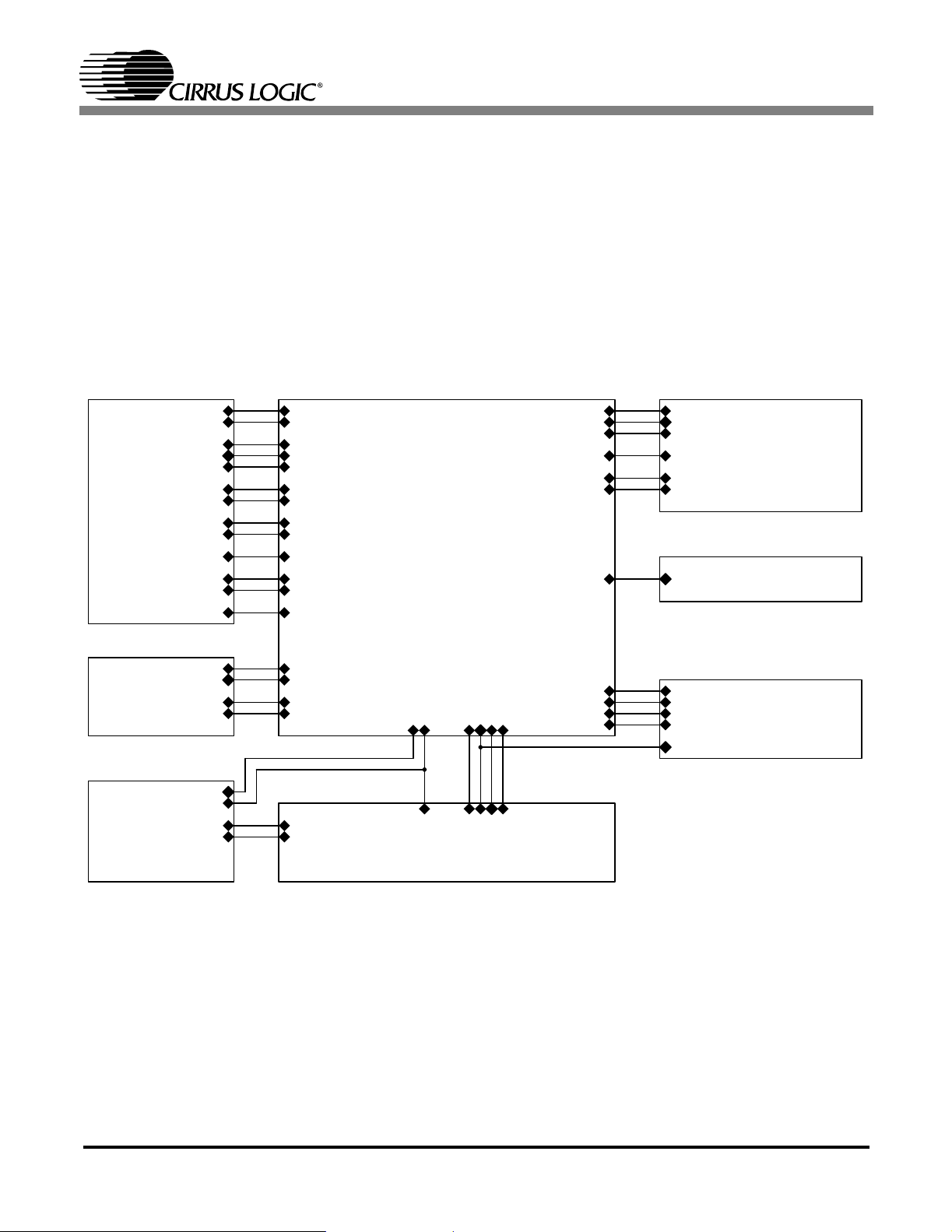
The block diagram in Figure 1 illustrates the interconnections between the schematic pages found at
the end of this document. Sections 2.1 through 2.8
describe the circuitry contained in these schematics.
2.1 CS4202 Audio Codec
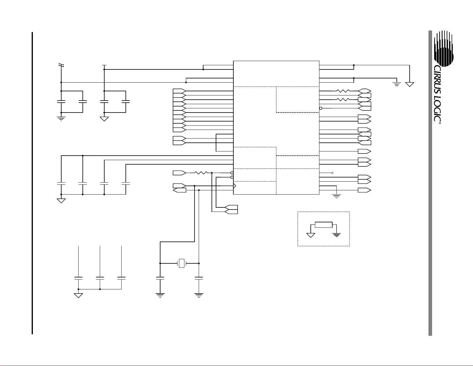
The CS4202 audio codec is shown in Figure 2. The
analog input signals to the CS4202 originate from
the inputs in Figure 3, while the analog outputs are
showninFigure4andFigure5.AFLT1and
AFLT2 (pins 29, 30) require 1000 pF NPO/COG
capacitors connected to analog ground. These capacitors provide a single pole lowpass filter to the
inputs of the CS4202 ADC. No other input filtering
is required.
The AC-Link may require series termination resistors to prevent reflections. These are normally
placed as close as possible to the transmitting end
of the AC-Link signal. The CS4202 SDATA_IN
(pin 8) and BIT_CLK (pin 6) outputs have 47 Ω series termination resistors.
The CS4202 is powered by separate analog and
digital power supplies, each with their own respective grounds. The AGND symbols refer to analog
ground and DGND symbols refer to digital ground.
For best results, connect the grounds together at a
single point with a 0.050 inch trace underneath the
CS4202. Each power pin requires an individual decoupling capacitor. These decoupling capacitors
are placed as close as possible to their respective
pins. The CS4202 audio codec uses a 0.1 µFceramic capacitor for each of the 3.3 V digital and
5 V analog supply pins.
2.2 Analog Inputs
The LINE_IN, VIDEO_IN, and AUX_IN stereo
inputs in Figure 3 are connected to 6 dB voltage dividers and AC-coupled to the CS4202 with 1 µF
capacitors to minimize low frequency roll-off. The
voltage divider allows input signal levels of up to
2 Vrms. The 6 dB dividers are for PC 99 compatibility and not required for PC 2001 compliance.
The microphone input is AC-coupled using a 1 µF
capacitor to minimize low frequency roll-off. The
microphone circuit provides low voltage phantom
power for electret microphones. Phantom power is
derived from the +5 V analog supply and provides
a maximum of 4.2 V under no load and a minimum
of 2.0 V under a 0.8 mA load, as required by
PC 2001 specifications.
DS549RD1A1 3
Page 4

CRD4202-1
The CS4202 features a pseudo-differential CD input that minimizes common mode noise and interference. Each CD signal acts as one side of the
differential input and CD_COM acts as the other
side.CD_COMisusedasthecommonreturnpath
for both the left and right channels.
2.3 Center, LFE, and Surround Outputs
The audio outputs in Figure 4 drive the rear speakers (surround), center speaker (CNT), and subwoofer (LFE) in six channel applications. These
four outputs are driven digitally from the CS4202
through two serial output ports and converted to analog audio through two high-performance CS4334
24-bit stereo DACs.
2.4 Front Channel and Headphone Outputs
Figure 5 details the Headphone and Line Output
circuits. The Line Outputs are the main analog outputs in a two channel system, and become the Front
Outputs in a six channel audio system.
The CS4202 has a built in headphone amplifier on
pins 39 and 41. These outputs are capable of driving headphones with impedances as low as 32 Ω.
The headphone outputs are AC-coupled through
220 µF capacitors. These large capacitor values
create excellent low frequency response even under
32 Ω loads.
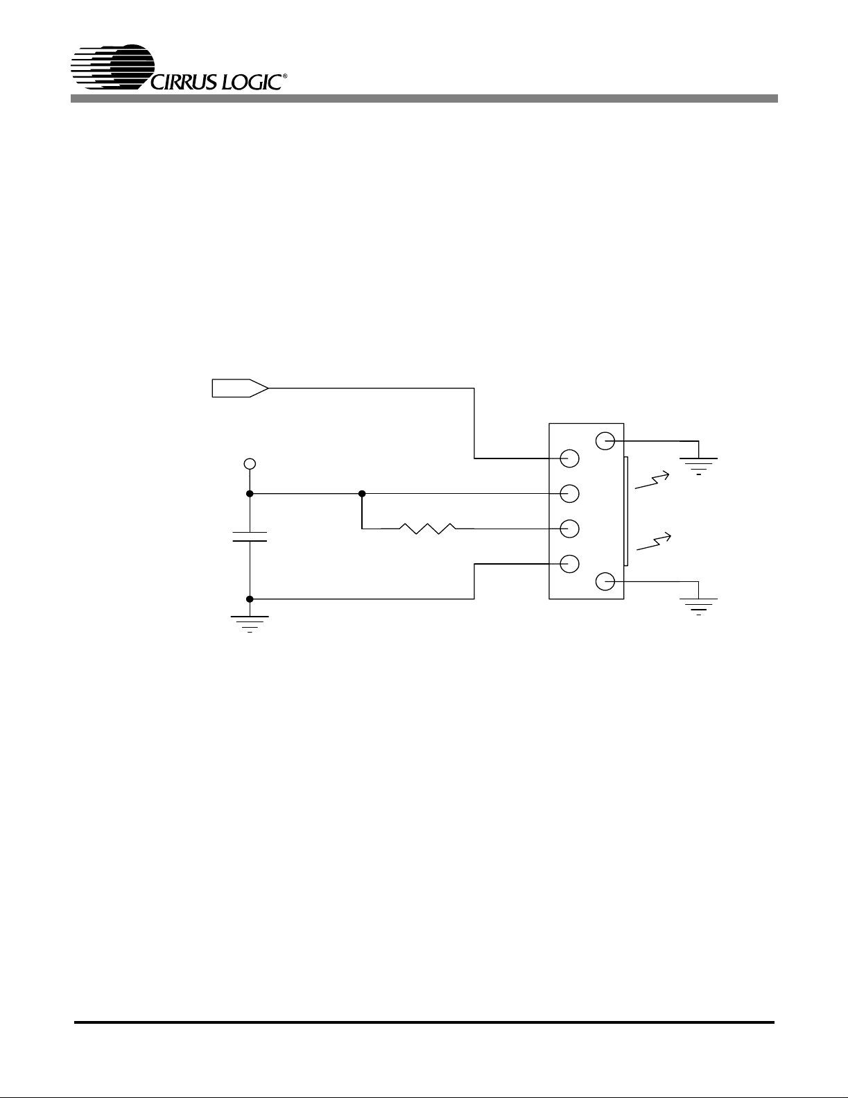
2.5 S/PDIF Optical Output
The S/PDIF (IEC-958) digital output shown in
Figure 6 is compatible with digital inputs on consumer devices such as Mini Disk recorders and
consumer stereo receivers. The S/PDIF output operates at a fixed sampling frequency of 48 kHz. It
uses an industry standard Toshiba TOTX-173 digital optical TOSLINK transmitter.
ed at OEMs, system manufacturers, and system integrators who wish take advantage of physically
separating their audio, modem, or LAN circuitry
from the PC motherboard. CNR accomplishes this
without the additional cost associated with the interface circuitry required for a PCI bus add-in card.
The CRD4202-1 uses the AC-Link, SMBus, and
power supply pins. The SMBus signals are connected to an AT24C02 EEPROM to provide Plugand-Play functionality for the CNR card. The EEPROM holds the Subsystem Vendor ID and Subsystem ID. It also contains other information for
implementing a Plug-and-Play CNR card. For additional information on the CNR design specifications, programming utilities, and information on
programming the EEPROM, visit the Intel
munications and Network Riser (CNR) homepage
at http://developer.intel.com/technology/cnr/.
®
Com-
2.7 Auto Demotion Circuit
The configuration of the codec on the CRD4202-1
will always be set as the primary audio codec.
However, it can automatically demote to secondary
in the presence of a motherboard codec when R54
ischangedto100kΩ (Figure 9). This feature is in
accordance with the AC '97 Codec Disable and De-
motion Rules.
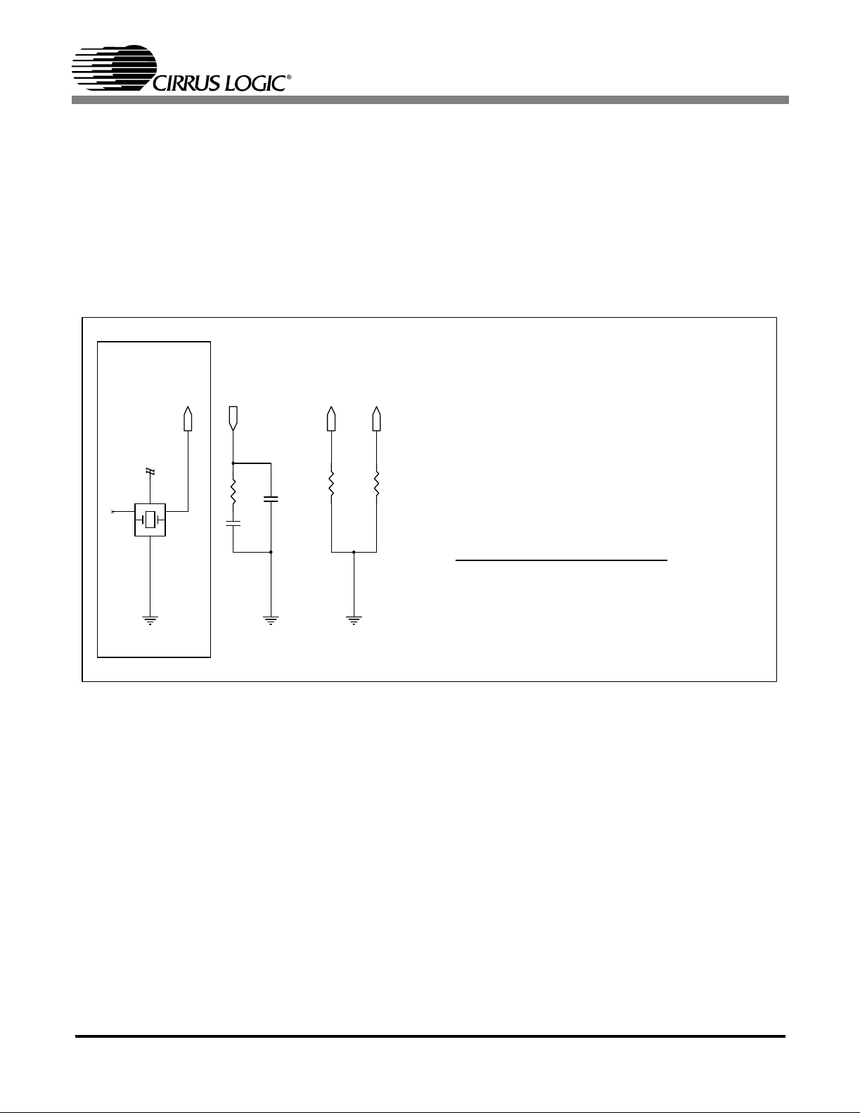
2.8 Phase Locked Loop (Optional)
The internal ADCs, DACs, and AC-Link operate at
a fixed 48k Hz rate. The CS4202 is clocked by a
24.576 MHz (±50 PPM) crystal. Footprint Y2 is for
an optional surface mounted clock oscillator for
use with the Phase Locked Loop (PLL) feature of
the CS4202. Figure 8 shows the population options
for implementing the PLL that will convert various
clock rates to the required 24.576 MHz operating
speed.
2.6 CNR Connector and EEPROM
The CNR connector is shown in Figure 7. CNR is a
motherboard interface that supports audio, modem,
and LAN subsystems. CNR applications are target-
4 DS549RD1A1
2.9 Component Selection
Great attention was given to the particular components used on the CRD4202-1 board with cost, per-
Page 5

CRD4202-1
formance, and package selection as the most
important factors. Listed are some of the guidelines
used in the selection of components:
• No components smaller than 0805 SMT package.
• Only single package passive components. No
resistor packs. This reduces the risk of crosstalk
between analog audio signals.
• All components except connectors are in surface mount packages.
2.10 EMI Components
Optional capacitors or inductors may be included
to help the board meet EMI compliance tests, such
as FCC Part 15. Choose these component values
according to individual requirements.
3. GROUNDING AND LAYOUT
The component layout and signal routing of the
CRD4202-1 provide a good model for developing
new CNR add-in card designs.
3.1 Partitioned Voltage and Ground
Planes
It is critical for good audio performance to separate
digital and analog sections to prevent digital noise
from affecting the performance of the analog circuits. The analog section of the CRD4202-1 is
physically isolated from the digital section with a
0.10 inch partition. Partitioning is defined as the
absence of copper on all PCB signal layers. The analog and digital sections have their own separate
ground planes. All analog components, power traces, and signal traces are routed over the analog
ground plane. Digital components, power traces,
and signal traces are not allowed to crossover into
the analog section.
out. The analog and digital ground planes must be
tied together externally for the CS4202 to maintain
proper voltage references. For best results, the two
ground planes are tied together with a single 0.050
inch trace under the CS4202 near its digital ground
pins.
Data converters are generally susceptible to noise
on the crystal pins. In order to reduce noise from
coupling onto these pins, the area around the
24.576 MHz crystal and its signal traces are filled
with copper on the top and bottom of the PCB and
attached to digital ground.
A separate chassis ground provides a noise-free
reference point for all of the EMI suppression components. The chassis ground plane is connected to
the analog ground plane at the external jacks.
3.2 AC-Link
According to the AC '97 revision 2.2 specification,
the AC-Link signals can have a maximum capacitance (including traces, connectors, and circuitry)
of 47.5 pF on BIT CLK and SDATA_IN (assuming
a single codec). If this capacitance is exceeded,
timing violations may occur and cause the system
to malfunction. In order to avoid adding excessive
capacitance, do not add any EMI capacitors to
ground on any of the AC-Link lines. In addition,
keep the trace length of the AC-Link as short as
possible. Keeping the AC-Link trace length under 8
inches is strongly recommend.
3.3 CS4202 Layout Notes
Refer to the CS4202 Data Sheet for analog and digital partitioning guidelines and bypass capacitor
placement. Pay special attention to the location of
bypass capacitors on REFFLT, AFLT1, AFLT2,
and the placement of the power supply capacitors.
The CS4202 audio codec is placed at the transition
point between the analog and digital ground planes.
The codec pins are grouped into analog and digital
sections to help facilitate printed circuit board lay-
DS549RD1A1 5
Page 6
4. REFERENCES
1) Intel®, Audio Codec '97 Component Specification, Revision 2.2, September, 2000.
http://developer.intel.com/ial/scalableplatforms/audio/index.htm/
®
2) Intel
, CNR Specification, Revision 1.1, October 18, 2000.
http://developer.intel.com/technology/cnr/
CRD4202-1
3) Cirrus Logic, CS4202 Audio Codec
'97 Data Sheet
http://www.cirrus.com/products
4) Steve Harris, Clif Sanchez, Personal Computer Audio Quality Measurements, Version 1.0
http://www.cirrus.com/pubs/meas100.pdf
5) Microsoft, PC Design Guidelines
,
http://www.microsoft.com/hwdev/desguid.htm
6) M. Montrose, Printed Circuit Board Design Techniques for EMC Compliance
(2nd edition), IEEE
Press, New York: 2000.
4.1 ADDENDUM
• Schematic drawings
• Layout drawings
• Bill of materials
6 DS549RD1A1
Page 7
CRD4202-1
ANALOG_IN
PLL (optional)
PRIM_SEC_SWITCH
LINE_IN_L
LINE_IN_R
CD_IN_L
CD_IN_R
CD_C
VIDEO_IN_L
VIDEO_IN_R
AUX_IN_L
AUX_IN_R
MIC_IN
PHONE_IN
MONO_OUT
PC_BEEP
XTAL_IN
XTAL_OUT
ID0#
ID1#
ASDIN
PRIM_DN#
ASDIN0
ASDIN1
CS4202
LINE_IN_L
LINE_IN_R
CD_IN_L
CD_IN_R
CD_C
VIDEO_IN_L
VIDEO_IN_R
AUX_IN_L
AUX_IN_R
MIC1
PHONE_IN
MONO_OUT
PC_BEEP
XTAL_IN
XTAL_OUT
ID0#
CNR_BUS
ASDIN0
ASDIN1
ANALOG_OUT
HP_OUT_L
HP_OUT_R
HP_OUT_C
GPIO2
LINE_OUT_L
LINE_OUT_R
SPDIF_OUT
SDOUT0
SDOUT1
ABITCLK
ASYNC
PRIM_DN#
ASDIN
PRIM_DN#
ASDOUT
ARST#
ASYNC
ARST#
ASDOUT
ABITCLK
SCLKID1#
LRCLK
HP_OUT_L
HP_OUT_R
HP_OUT_C
GPIO2
LINE_OUT_L
LINE_OUT_R
SPDIF_OUT
SPDIF_TX
SERIAL_PORT
SDOUT0
SDOUT1
SCLK
LRCLK
MCLK
Figure 1. Block Di agram
DS549RD1A1 7
Page 8
8 DS549RD1A1
U1 CS4202
+3.3VD
DGND
C1
0.1uF
Z5U
C5
2.2uF
Y5V
C2
0.1uF
Z5U
C6
0.1uF
X7R
+5VA
AGND
C3
0.1uF
Z5U
C7
1000pF
NPO
C4
0.1uF
Z5U
C8
NPO
PC_BEEP
PHONE_IN
AUX_IN_L
AUX_IN_R
VIDEO_IN_L
VIDEO_IN_R
CD_IN_L
CD_C
CD_IN_R
MIC1
LINE_IN_L
LINE_IN_R
PRIM_DN#
XTAL_IN
XTAL_OUT
R55 0
25
38
1
9
12
13
14
15
16
17
18
19
20
21
22
23
24
28
27
29
30
45
46
2
3
AVdd1
AVdd2
DVdd1
DVdd2
PC_BEEP
PHONE
AUX_L
AUX_R
VIDEO_IN_L
VIDEO_IN_R
CD_L
CD_C
CD_R
MIC1
MIC2
LINE_IN_L
LINE_IN_R
Vrefout
REFFLT
AFLT1
AFLT2
ID0#
ID1#
XTL_IN
XTL_OUT
AVss1
AVss2
DVss1
DVss2
BIT_CLK
SDATA_OUT
SDATA_IN
SYNC
RESET#
LINE_OUT_L
LINE_OUT_R
HP_OUT_L
HP_OUT_C
HP_OUT_R
GPIO2
MONO_OUT
SPDIF_OUT
EAPD/SCLK
HPCFG
GPIO0/LRCLK
GPIO1/SDOUT
GPIO3
GPIO4/SDO2
26
42
4
7
6
R1 47
5
8
R2 47
10
11
35
36
39
40
41
32
37
48
47
31
43
44
33
34
ABITCLK
ASDOUT
ASDIN
ASYNC
ARST#
LINE_OUT_L
LINE_OUT_R
HP_OUT_L
HP_OUT_C
HP_OUT_R
GPIO2
MONO_OUT
SPDIF_OUT
SCLK
LRCLK
SDOUT0
SDOUT1
DGND
AGND
AGND
LINE_OUT_L
C11
1000pF
NPO
LINE_OUT_R
C12
1000pF
NPO
MONO_OUT
C13
1000pF
NPO
Y1
24.576 MHz
DGND
C14
22pF
NPO
C15
22pF
NPO
DGNDAGND
Figure 2. CS4202 Audio Codec
ID1#
ID0#
DGND
GND TIE 0.050 inches
AGND
DGND
For 6 channel
configuration GPIO3 (pin 33)
is tied to
DGND.
CRD4202-1
Page 9

DS549RD1A1 9
CD IN
J2
VIDEO IN
J4
L1
4
3
2
1
4
3
2
1
31@100MHz
L2
31@100MHz
L3
31@100MHz
L4
31@100MHz
L5
31@100MHz
AGND
AGNDAGNDAGND AGND
R5 100K
R9 100K
R12 100K
R13 6.8K
R16 6.8K
R18 6.8K
R19 6.8K
C16 1uF
C18 1uF
C22 1uF
C23 1uF
C25 1uF
ELEC
+
ELEC
+
ELEC
+
ELEC
+
ELEC
+
CD_IN_R
CD_C
CD_IN_L
VIDEO_IN_R
VIDEO_IN_L
LINE IN
J1
Connect CGND
to AGND at
the jack
MIC IN
J3
Connect CGND
to AGND at
the jack
+
C28
10uF
ELEC
AGND
AGND
R4 6.8K
R6 6.8K
R8 6.8K
R10 6.8K
R15 1.5K
4
3
5
2
1
C19
C20
100pF
100pF
NPO
NPO
AGND
CGND
4
3
5
2
1
C26
100pF
NPO
R14 2.2K
C27
100pF
NPO
+5VA
C24 1uF
C17 1uF
C21 1uF
ELEC
+
ELEC
+
ELEC
+
LINE_IN_R
LINE_IN_L
MIC_IN
AGND
AUX IN BEEP IN
J5
4
3
2
1
L6
31@100MHz
L8
31@100MHz
AGND
R20 6.8K
R22 6.8K
R24 6.8K
R25 6.8K
AGNDAGND
C30 1uF
C33 1uF
ELEC
+
ELEC
+
AUX_IN_R
AUX_IN_L
J6
INTERNAL MODEM CONNECTION
J7
4
3
2
1
L9
31@100MHz
L10
31@100MHz
AGND
R26 6.8K
R27 6.8K
AGND
R28 0
R29 47K
C34 1uF
C35 1uF
AGND
ELEC
+
ELEC
+
PHONE_IN
MONO_OUT
Figure 3. Analog Inputs
AGND
AGND
Z5U
R23
C32
4.7K
2700pF
X7R
AGND
PC_BEEP
-3 dB corners at 60 Hz
and 13.8 kHz
(Ri >= 28 kOhm)
AGND
CGND
L7
31@100MHz
2
1
DGND
R21 47K C31 0.1uF
CRD4202-1
Page 10
10 DS549RD1A1
+5VA
SURROUND
AGND
JACK
J8
4
3
5
2
1
Connect CGND
to AGND at
the jack
CNT/LFE
JACK
J9
4
3
5
2
1
Connect CGND
to AGND at
the jack
SDOUT0
SDOUT1
SCLK
LRCLK
MCLK
U2 CS4334
1
SDATA
2
DEM#/SCLK
3
LRCK
4
MCLK
+5VA
C40
+ C42
10uF
ELEC
AGND
U3 CS4334
1
SDATA
2
DEM#/SCLK
3
LRCK
4
MCLK
C41
0.1uF
Z5U
AOUTR
AGND
AOUTL
AOUTR
AGND
AOUTL
VA+
VA+
0.1uF
Z5U
C36 1uF
5
7
6
8
R32
270K
AGND AGND
5
7
6
8
R38
270K
AGND
+
ELEC
C37 1uF
+
ELEC
R33
270K
C43 1uF
+
ELEC
C44 1uF
+
ELEC
R39
270K
R40
R34
47K
47K
R30 560
R31 560
R35
47K
R36 560
R37 560
R41
47K
C38
2700pF
X7R
CGND
C45
2700pF
X7R
C39
2700pF
X7R
C46
2700pF
X7R
AGND
Figure 4. Center Channel, Surround, and Sub-Woofer Outputs
CGND
AGNDAGND
CRD4202-1
Page 11

DS549RD1A1 11
LINE_OUT_R
LINE_OUT_L
C48 1uF
+
ELEC
C49 1uF
+
ELEC
R44
220K
R45
220K
C50
100pF
NPO
C51
100pF
NPO
LINE OUT
JACK
J10
4
3
5
2
1
Connect CGND
to AGND at
the jack
GPIO2
HP_OUT_L
HP_OUT_R
HP_OUT_C
C54 220uF
+
ELEC
C55 220uF
+
ELEC
C56 1uF
+
ELEC
AGND
R48
10K
AGND DGND
R49
10K
CGND
C57
100pF
NPO
CGND
Figure 5. Front Channel and Headphone Sense Output
+3.3VD
C58
100pF
NPO
R56
10K
AGND
AGND
HEADPHONE
JACK
J11
7
6
2
3
1
Connect CGND
to AGND at
the jack
CRD4202-1
Page 12
SPDIF_TX
+5VD
CRD4202-1
J12
5
4
DGND
C59
0.1uF
Z5U
R50 8.2K
Figure 6. S/PDIF Optical Output
3
2
1
TOTX-173
DGND
6
DGND
12 DS549RD1A1
Page 13

DS549RD1A1 13
PRIM_DN#
ASYNC
ASDOUT
ABITCLK
+3.3VD
DGND
P1
B1
reserved
B2
reserved
B3
reserved
B4
GND
B5
reserved
B6
reserved
B7
GND
B8
LAN_TXD1
B9
LAN_RSTSYNC
B10
GND
B11
LAN_RXD2
B12
LAN_RXD0
B13
GND
B14
reserved
B15
+5Vdual
DGND
B16
B17
B18
B19
B20
B21
B22
B23
B24
B25
B26
B27
B28
B29
B30
CNR Connector
USB_OC#
GND
-12V
+3.3VD
GND
EE_DOUT
EE_SHCLK
GND
SMB_A0
SMB_SCL
CDC_DN_ENAB#
GND
AC97_SYNC
AC97_SDATA_OUT
AC97_BITCLK
C61
0.1uF
Z5U
C62
+ C63
10uF
ELEC
TP1 TP2 TP3 TP4 TP5
reserved
reserved
reserved
reserved
LAN_TXD2
LAN_TXD0
LAN_RXD1
reserved
+3.3Vdual
AC97_RESET#
AC97_SDATA_IN2
AC97_SDATA_IN1
AC97_SDATA_IN0
GND
GND
GND
LAN_CLK
USB+
GND
USB+12V
GND
+5VD
GND
EE_DIN
EE_CS
SMB_A1
SMB_A2
SMB_SDA
GND
A1
A2
A3
A4
A5
A6
A7
A8
A9
A10
A11
A12
A13
A14
A15
A16
A17
A18
A19
A20
A21
A22
A23
A24
A25
A26
A27
A28
A29
A30
DGND
+12VD
TP6
DGND
0.1uF
Z5U
ARST#
ASDIN1
ASDIN0
+5VD
C64
+
10uF
ELEC
+3.3VD
2
3
5
6
1
U5
A1
A2
SDA
SCL
A0
AT24C02
8
Vcc
WP
Vss
7
4
DGND
C60
0.1uF
Z5U
U6
DGND
C65
0.1uF
Z5U
1
IN
+
10uF
ELEC
2
OUT
GND
MC78M05C
Connect AGND to DGND with a 50 mil trace near the codec.
Connect CGND to DGND with a 50 mil trace near the finger
edge of the board.
+5VA+12VD
3
C67
+C66
10uF
ELEC
AGND
Figure 7. CNR Connector
CRD4202-1
Page 14
Test Clock Only
CRD4202-1
OPTIONAL PLL (Phase Locked Loop)
XTAL_IN
+3.3VD
31
2 4
Y2
NO POP
DGND DGND
XTAL_OUT
R51
NO POP
C68
NO POP
C69
NO POP
ID1#
R52
NO POP
DGND
ID0#
R53
NO POP
For PLL operation:
1)
Populate R54 = 1K
DO NOT populate: Y1, C14, C15, and R55
2)
Apply external oscillator to XTAL_IN (pin 2)
3)
(CRD4202-1 can use test oscillator on Y2: ECS-8FA3)
Populate R51, R52, R53, C68, and C69 according to
4)
your input clock rate:
clock rate (MHz) R51 R52 R53 C68 C69
14.31818 2.2K NO POP 0 ohm 0.022uF 220pF
24.576 NO POP NOPOP NO POP NO POP NO POP
27 2.2K 0 ohm NO POP 0.022uF 220pF
48 2.2K 0 ohm 0ohm 0.022uF 220pF
Figure 8. Phase Locked Loop
14 DS549RD1A1
Page 15

+3.3VD
CRD4202-1
R54 = 1K forces
motherboard codec(s)
to be held in RESET
PRIM_DN#
R54
1K
U7
TC7SZ125FU
U8
TC7SZ126FU
5
2 4
1
3
5
1
2 4
3
DGND
+3.3VD
DGND
C70
0.1uF
X7R
C71
0.1uF
X7R
ASDIN1
ASDIN0ASDIN
DO NOT use this circuit for motherboard designs. This ci rcuit is strictly for CNR cards.
For motherboard designs:
connect ASDIN to ASDIN0 if primary codec,
connect ASDIN to ASDIN1 if secondary codec.
Replace R54 with 100K for automatic demotion
when used with primary motherboard codec(s).
Figure 9. Auto Demotion and Serial Buffers
DS549RD1A1 15
Page 16

CRD4202-1
Figure 10. PCB Layout: Top Assembly Drawing
16 DS549RD1A1
Page 17

CRD4202-1
Figure 11. PCB Layout: Top Layer
DS549RD1A1 17
Page 18

CRD4202-1
Figure 12. PCB Layout: Bottom Layer
18 DS549RD1A1
Page 19

CRD4202-1
Figure 13. PCB Layout: Drill Drawing
DS549RD1A1 19
Page 20

CRD4202-1
Figure 14. PCB Layout: Top Silkscreen
20 DS549RD1A1
Page 21
DS549RD1A1 21
5. BILL OF MATERIALS
Item Quantity Reference Manufacturer Part Number Description
1 12 C1,C2,C3,C4,C31,C41,
C42,C59,C60,C61,C63,C65
2 1 C5 KEMET C1206C225M8VAC
3 3 C6,C70,C71 KEMET C0805C104K5RAC
4 5 C7,C8,C11,C12,C13 KEMET C0805C102K5GAC CAP, 0805, C0G, 1000 pF, 10%, 50V
5 2 C14,C15 KEMET C0805C220K5GAC CAP, 0805, C0G, 22 pF, 10%, 50V
6 19 C16,C17,C18,C21,C22,
C23,C24,C25,C30,C33,
C34,C35,C36,C37,C43,
C44,C48,C49,C56
7 4 C19,C20,C26,C27 KEMET C0805C101J5GAC CAP, 0805, COG, 100 pF, 5%, 50V
8 6 C28,C40,C62,C64,C66,C67 PANASONIC ECE-V1CA100R
9 5 C32,C38,C39,C45,C46 KEMET C0805C272K5RAC CAP, 0805, X7R, 2700 pF, 10%, 50V
10 4 C50,C51,C57,C58 KEMET C0805C101J5GAC CAP, 0805, C0G, 100 pF, 5%, 50V
11 2 C54,C55 PANASONIC ECE-V0GA221P
KEMET C0805C104M5UAC
PANASONIC ECE-V1HA010R
CAP, 0805, Z5U, 0.1
CAP, 1206, Y5V, 2.2
CAP, 0805, X7R, 0.1
CAP, SMT B, ELEC, 1
CAP, SMT B, ELEC, 10
CAP, SMT D, ELEC, 220
µF, 20%, 50V
µF, 20%, 10V
µF, 10%, 50V
µF, 20%, 50V
µF, 20%, 16V
µF, 20%, 4V
12 2 C68,C69 NO POP NO POP NO POP
13 5 J1,J3,J8,J9,J10 A/D ELEC-
TRONICS
14 4 J2,J4,J5,J7 MOLEX 70553-0003 HDR, 4X1, 0.025" PIN, 0.1" CTR, 15u" AU
15 1 J6 MOLEX 70553-0036 HDR, 2X1, 0.025" PIN, 0.1" CTR, 150u" SN/PB
16 1 J11 SINGATRON 2SJ-09075N53 CONN, 1/8" SINGLE SW. STEREO PHONE
17 1 J12 TOSHIBA TOTX173 CONN, OPTICAL TOSLINK TRANSMITTER
3570-50 CONN, 1/8" DOUBLE SW. STEREO PHONE
JACK
JACK W/INSULATOR
CRD4202-1
Page 22
22 DS549RD1A1
18 10 L1,L2,L3,L4,L5,L6,L7,L8,
L9,L10
19 1 P1 NONE NONE CNR BUS CONNECTOR
20 2 R2,R1 PHILIPS 9C08052A47R0J RES, SO, 0805, 47, 5%, 1/10W, METAL FILM
TDK HF50ACB321611-T IND, FBEAD, 1206, 31@100MHz, 25%
21 14 R4,R6,R8,R10,R13,R16,
R18,R19,R20,R22,R24,
R25,R26,R27
22 3 R5,R9,R12 PHILIPS 9C08052A1003J RES, SO, 0805, 100K, 5%, 1/10W, METAL FILM
23 1 R14 PHILIPS 9C08052A2201J RES, SO, 0805, 2.2K, 5%, 1/10W, METAL FILM
24 1 R15 PHILIPS 9C08052A1501J RES, SO, 0805, 1.5K, 5%, 1/10W, METAL FILM
25 6 R21,R29,R34,R35,R40,R41 PHILIPS 9C08052A4702J RES, SO, 0805, 47K, 5%, 1/10W, METAL FILM
26 1 R23 PHILIPS 9C08052A4701J RES, SO, 0805, 4.7K, 5%, 1/10W, METAL FILM
27 2 R28,R55 PHILIPS 9C08052A0R00J RES, SO, 0805, 0, 5%, 1/10W, METAL FILM
28 4 R30,R31,R36,R37 PHILIPS 9C08052A5600J RES, SO, 0805, 560, 5%, 1/10W, METAL FILM
29 4 R32,R33,R38,R39 PHILIPS 9C08052A2703J RES, SO, 0805, 270K, 5%, 1/10W, METAL FILM
30 2 R45,R44 PHILIPS 9C08052A2203J RES, SO, 0805, 220K, 5%, 1/10W, METAL FILM
31 3 R48,R49,R56 PHILIPS 9C08052A1002J RES, SO, 0805, 10K, 5%, 1/10W, METAL FILM
32 1 R50 PHILIPS 9C08052A8201J RES, SO, 0805, 8.2K, 5%, 1/10W, METAL FILM
33 3 R51,R52,R53 NO POP NO POP NO POP
PHILIPS 9C08052A6801F RES, SO, 0805, 6.8K, 1%, 1/10W, METAL FILM
34 1 R54 PHILIPS 9C08052A1001J RES, SO, 0805, 1K, 5%, 1/10W, METAL FILM
35 6 TP1,TP2,TP3,TP4,TP5,TP6 KEYSTONE 5015 mini SMT test point
36 1 U1 Cirrus Logic CS4202-JQ IC, TQFP, AC '97 2.2 SERIAL CODEC W/ HP
AMP + SRC
37 2 U2,U3 Cirrus Logic CS4334-KS IC, SO, SOIC8, STEREO DAC, 24 BITS
CRD4202-1
Page 23

DS549RD1A1 23
38 1 U5 ATMEL AT24C02N-10SC-
2.7
39 1 U6 MOTOROLA MC78M05CDT IC, SO, +5V REGULATOR, DPAK, 4%, 500mA
40 1 U7 TOSHIBA TC7SZ125FU IC, SSOP5-P-0.65A, single 3 state buffer, 2.6ns
41 1 U8 TOSHIBA TC7SZ126FU IC, SSOP5-P-0.65A, single 3 state buffer, 2.6ns
42 1 Y1 FOX FS24.576 XTAL, 24.576MHz, HC49S, Fund Mode, Par Res
43 1 Y2 NOPOP NOPOP NOPOP
IC, SO, SOIC8, SERIAL EEPROM, 256 x 8, 2.7V
CRD4202-1
Page 24

 Loading...