

Page 1

COM20020I 3.3V
5Mbps ARCNET (ANSI
878.1) Controller with
2K x 8 On-Chip RAM
Datasheet
Product Features
New Features:
- Data Rates up to 5 Mbps
- Programmable Reconfiguration Times
28 Pin PLCC and 48 Pin TQFP Packages;
Lead-free RoHS Compliant Packages also
available
Ideal for Industrial/Factory/Building Automation
and Transportation Applications
Deterministic, (ANSI 878.1), Token Passing
ARCNET Protocol
Minimal Microcontroller and Media Interface
Logic Required
Flexible Interface For Use With All
Microcontrollers or Microprocessors
Automatically Detects Type of Microcontroller
Interface
2Kx8 On-Chip Dual Port RAM
Command Chaining for Packet Queuing
Sequential Access to Internal RAM
Software Programmable Node ID
Eight, 256 Byte Pages Allow Four Pages TX and
RX Plus Scratch-Pad Memory
Next ID Readable
Internal Clock Scaler and Clock Multiplier for
Adjusting Network Speed
o
Operating Temperature Range of -40
Self-Reconfiguration Protocol
Supports up to 255 Nodes
Supports Various Network Topologies (Star, Tree,
Bus...)
CMOS, Single +3.3V Supply
Duplicate Node ID Detection
Powerful Diagnostics
Receive All Packets Mode
Flexible Media Interface:
- Traditional Hybrid Interface For Long
Distances up to Four Miles at 2.5Mbps
- RS485 Differential Driver Interface For Low
Cost, Low Power, High Reliability
C to +85oC
SMSC COM20020I 3.3V 1 Revision 12-06-06
DATASHEET
Page 2

5Mbps ARCNET (ANSI 878.1) Controller with 2K x 8 On-Chip RAM
ORDERING INFORMATION
Order Numbers:
COM20020I3VLJP for 28 pin PLCC package
COM20020I3V-DZD for 28 pin PLCC package lead-free RoHS co mpliant package
COM20020I3V-HD for 48 pin TQFP package
COM20020I3V-HT for 48 pin TQFP lead-free RoHS compliant package
Hauppauge, NY 11788
(631) 435-6000
FAX (631) 273-3123
80 Arkay Drive
Copyright © 2006 SMSC or its subsidiaries. All rights reserved.
Circuit diagrams and other information relating to SMSC products are included as a means of illustrating typical applications. Consequently, complete
information sufficient for construction purposes is not necessarily given. Although the information has been checked and is believed to be accurate, no
responsibility is assumed for inaccuracies. SMSC reserves the right to make changes to specifications and product descriptions at any time without
notice. Contact your local SMSC sales office to obtain the latest specifications before placing your product order. The provision of this information does
not convey to the purchaser of the described semiconductor devices any licenses under any patent rights or other intellectual property rights of SMSC
or others. All sales are expressly conditional on your agreement to the terms and conditions of the most recently dated version of SMSC's standard
Terms of Sale Agreement dated before the date of your order (the "Terms of Sale Agreement"). The product may contain design defects or errors
known as anomalies which may cause the product's functions to deviate from published specifications. Anomaly sheets are available upon request.
SMSC products are not designed, intended, authorized or warranted for use in any life support or other application where product failure could cause
or contribute to personal injury or severe property damage. Any and all such uses without prior written approval of an Officer of SMSC and further
testing and/or modification will be fully at the risk of the customer. Copies of this document or other SMSC literature, as well as the Terms of Sale
Agreement, may be obtained by visiting SMSC’s website at http://www.smsc.com. SMSC is a registered trademark of Standard Microsystems
Corporation (“SMSC”). Product names and company names are the trademarks of their respective holders.
SMSC DISCLAIMS AND EXCLUDES ANY AND ALL WARRANTIES, INCLUDING WITHOUT LIMITATION ANY AND ALL IMPLIED WARRANTIES
OF MERCHANTABILITY, FITNESS FOR A PARTICULAR PURPOSE, TITLE, AND AGAINST INFRINGEMENT AND THE LIKE, AND ANY AND
ALL WARRANTIES ARISING FROM ANY COURSE OF DEALING OR USAGE OF TRADE. IN NO EVENT SHALL SMSC BE LIABLE FOR ANY
DIRECT, INCIDENTAL, INDIRECT, SPECIAL, PUNITIVE, OR CONSEQUENTIAL DAMAGES; OR FOR LOST DATA, PROFITS, SAVINGS OR
REVENUES OF ANY KIND; REGARDLESS OF THE FORM OF ACTION, WHETHER BASED ON CONTRACT; TORT; NEGLIGENCE OF SMSC
OR OTHERS; STRICT LIABILITY; BREACH OF WARRANTY; OR OTHERWISE; WHET HER OR NOT ANY REMEDY OF BUYER IS HELD TO
HAVE FAILED OF ITS ESSENTIAL PURPOSE, AND WHETHER OR NOT SMSC HAS BEEN ADVISED OF THE POSSIBILITY OF SUCH
DAMAGES.
Revision 12-06-06 SMSC COM20020I 3.3V
2
DATASHEET
Page 3

5Mbps ARCNET (ANSI 878.1) Controller with 2K x 8 On-Chip RAM
TABLE OF CONTENTS
2.0
GENERAL DESCRIPTION..............................................................................................................................5
3.0 PIN CONFIGURATIONS.................................................................................................................................6
4.0 DESCRIPTION OF PIN FUNCTIONS FOR TQFP ..........................................................................................8
5.0 PROTOCOL DESCRIPTION.........................................................................................................................11
5.1 NETWORK PROTOCOL ..................................................................................................................................11
5.2 DATA RATES ...............................................................................................................................................11
5.3 NETWORK RECONFIGURATION.......................................................................................................................12
5.4 BROADCAST MESSAGES...............................................................................................................................12
5.5 EXTENDED TIMEOUT FUNCTION.....................................................................................................................12
5.6 LINE PROTOCOL ..........................................................................................................................................13
6.0 SYSTEM DESCRIPTION...............................................................................................................................15
6.1 MICROCONTROLLER INTERFACE ....................................................................................................................15
6.2 TRANSMISSION MEDIA INTERFACE .................................................................................................................19
7.0 FUNCTIONAL DESCRIPTION...................................................................................................................... 24
7.1 MICROSEQUENCER ......................................................................................................................................24
7.2 INTERNAL REGISTERS...........................................................................................................................25
7.3 INTERNAL RAM ............................................................................................................................................35
7.4 COMMAND CHAINING....................................................................................................................................40
7.5 INITIALIZATION SEQUENCE ............................................................................................................................42
7.6 IMPROVED DIAGNOSTICS ..............................................................................................................................42
8.0 OPERATIONAL DESCRIPTION...................................................................................................................45
8.1 MAXIMUM GUARANTEED RATINGS*................................................................................................................45
8.2 DC ELECTRICAL CHARACTERISTICS ...............................................................................................................45
9.0 TIMING DIAGRAMS......................................................................................................................................48
10.0 PACKAGE OUTLINES..................................................................................................................................60
11.0 APPENDIX A.................................................................................................................................................62
12.0 APPENDIX B.................................................................................................................................................65
12.1 SOFTWARE IDENTIFICATION OF THE COM20020I REV B, REV C AND REV D .....................................................65
LIST OF FIGURES
Figure 1 - COM20020I OPERATION ...........................................................................................................................10
Figure 2 - MULTIPLEXED, 8051-LIKE BUS INTERFACE WITH RS-485 INTERFACE...............................................16
Figure 3 - NON-MULTIPLEXED, 6801-LIKE BUS INTERFACE WITH RS-485 INTERFACE......................................17
Figure 4 - HIGH SPEED CPU BUS TIMING - INTEL CPU MODE...............................................................................18
Figure 5 - COM20020 I NETWORK USING RS-485 D I F F ERENTIAL TR A NSCEIVERS................................................20
Figure 6 - DIPULSE WAVEFORM FOR DATA OF 1-1-0.............................................................................................20
Figure 7 - INTERNAL BLOCK DIAGRAM....................................................................................................................22
Figure 8 – SEQUENTIAL ACCESS OPERATION........................................................................................................35
Figure 9 – RAM BUFFER PACKET CONFIGURATION ..............................................................................................38
Figure 10 - COMMAND CHAINING STATUS REGISTER QUEUE...............................................................................40
Figure 11 - MULTIPLEXED BUS, 68XX-LIKE CONTROL SIGNALS; READ CYCLE..................................................48
Figure 12 - MULTIPLEXED BUS, 80XX-LIKE CONTROL SIGNALS; READ CYCLE..................................................49
Figure 13 - MULTIPLEXED BUS, 68XX-LIKE CONTROL SIGNALS; WRITE CYCLE.................................................50
SMSC COM20020I 3.3V Page 3 Revision 12-06-06
DATASHEET
Page 4

5Mbps ARCNET (ANSI 878.1) Controller with 2K x 8 On-Chip RAM
Figure 14 - MULTIPLEXED BUS, 80XX-LIKE CONTROL SIGNALS; WRITE CYCLE.................................................51
Figure 15 - NON-MULTIPLEXED BUS, 80XX-LIKE CONTROL SIGNALS; READ CYCLE.........................................52
Figure 16 - NON-MULTIPLEXED BUS, 80XX-LIKE CONTROL SIGNALS; READ CYCLE.........................................53
Figure 17 - NON-MULTIPLEXED BUS, 68XX-LIKE CONTROL SIGNALS; READ CYCLE.........................................54
Figure 18 - NON-MULTIPLEXED BUS, 68XX-LIKE CONTROL SIGNALS; READ CYCLE.........................................55
Figure 19 - NON-MULTIPLEXED BUS, 80XX-LIKE CONTROL SIGNALS; WRITE CYCLE .......................................56
Figure 20 - NON-MULTIPLEXED BUS, 68XX-LIKE CONTROL SIGNALS; WRITE CYCLE .......................................57
Figure 21 – NORMAL MODE TRANSMIT OR RECEIVE TIMING...............................................................................58
Figure 22 – BACKPLANE MODE TRANSMIT OR RECEIVE TIMING.........................................................................58
Figure 23 – TTL INPUT TIMING ON XTAL1 PIN.........................................................................................................59
Figure 24 – RESET AND INTERRUPT TIMING...........................................................................................................59
Figure 25 - 28 PIN PLCC PACKAGE DIMENSIONS ...................................................................................................60
Figure 26 - 48 PIN TQFP PACKAGE OUTLINE...........................................................................................................61
Figure 27 - EFFECT OF THE EF BIT ON THE TA/RI BIT...........................................................................................63
LIST OF TABLES
Table 1 - Typical Media................................................................................................................................................23
Table 2 - Read Register Summary...............................................................................................................................24
Table 3 - Write Register Summary...............................................................................................................................25
Table 4 - Status Register..............................................................................................................................................28
Table 5 - Diagnostic Status Re gister.............................................................................................................................29
Table 6 - Command Register........................................................................................................................................30
Table 7 - Address Pointer High Register.......................................................................................................................31
Table 8 - Address Pointer Low Register........................................................................................................................31
Table 9 - Sub Address Reg i ster...................................................................................................................................31
Table 10 - Configuration Register ................................................................................................................................31
Table 11 - Setup 1 Register..........................................................................................................................................33
Table 12 - Setup 2 Register..........................................................................................................................................34
Revision 12-06-06 SMSC COM20020I 3.3V
4
DATASHEET
Page 5

5Mbps ARCNET (ANSI 878.1) Controller with 2K x 8 On-Chip RAM
2.0 General Description
SMSC's COM20020I is a member of the family of Embedded ARCNET Controllers from Standard Microsystems
Corporation. The device is a general purpose communications controller for networking microcontrollers and intelligent
peripherals in industrial, automotive, and embedded control environments using an ARCNET
flexible microcontroller and media interfaces, eight-page message support, and extended temperature range of the
COM20020I make it the only true network controller optimized for use in industrial, embedded, and automotive
applications. Using an ARCNET protocol engine is the ideal solution for embedded control applications because it
provides a deterministic t oken-passing protocol, a hig hly reliable and proven net working scheme, a nd a data rate of u p
to 5 Mbps when using the COM20020I.
A token-passing protocol provides predictable response times because each network event occurs within a
predetermined time interval, based upon the number of nodes on the network. The deterministic nature of ARCNET is
essential in real time applications. T he integration of the 2Kx8 RAM buffer on-chip, the Command Chaining feature, the
5 Mbps maximum data rate, and the internal diagnostics make the COM20020I the highest performance embedded
communications device available. With only one COM20020I and one microcontroller, a complete communications node
may be implemented.
For more details on the ARCNET protocol engine and traditional dipulse signaling schemes, please refer
to the ARCNET Local Area Network Standard
ARCNET Designer's Handbook
For more detailed information o n cabling optio ns including RS485 , transforme r-coupled RS- 485 and Fiber
Optic interfaces, please refer to the following technical note which is available from Standard
Microsystems Corporation: Techn ical Not e 7- 5 - Cabling Guid elin es for the COM20 020I ULA NC.
, available from Datapoint Corporation.
, available from Standard Microsystems Corporation or the
protocol engine. The
SMSC COM20020I 3.3V Page 5 Revision 12-06-06
DATASHEET
Page 6

3.0 PIN CONFIGURATIONS
5Mbps ARCNET (ANSI 878.1) Controller with 2K x 8 On-Chip RAM
A0/nMUX
A2/ALE
1
2
A1
3
AD0
4
AD1
5
AD2
6
D3
7
D4
8
D5
9
10
D6
11
D7
12
VSS
Package: 28-Pin PLCC
Pac kag es: 24-Pin DIP or 28-Pin PLCC
Ordering Information:
Ordering Information:
COM20020 I P
COM20019
N
I
T
E
N
S
24
VDD
23
nRD/nDS
22
nWR/DIR
21
nCS
20
nINTR
19
nRESET IN
18
nTXEN
17
RXIN
nPULSE2
16
15
nPULSE1
14
XTAL2
13
XTAL1
I
P
PACKAGE TYPE: P = Plastic , LJP = PLCC
PACKAGE TYPE: P = Plastic, LJP = PLCC
nWR/DIR
nRD/nDS
VDD
A0/nMUX
A1
A2/ALE
AD0
TR
S
N
I
C
n
n
25 24 23 22 21 20 19
26
27
28
1
2
3
4
567891011
2
1
D
D
A
A
E
S
E
S
R
TX
n
V
n
3
S
D
S
V
TEMP RANGE: (Blank) = Commercial: 0°C to +70°C
TEMP RANGE: 1 = Industrial: -40° C to 75° C
I = Industrial: -40°C to +85°C
DEVICE TYPE: 20020 = Universal Local Area Network
DEVICE TYPE: 20019 = Universal Local Area Network Controller
(with 2K x 8 RAM)
(with 2K x 8 RAM)
2
E
S
L
N
I
U
X
P
R
n
nPULSE 1
18
17
XTAL2
16
XTAL1
15
VDD
VSS
14
13
N/C
12
D7
6
5
4
D
D
D
Revision 12-06-06 SMSC COM20020I 3.3V
6
DATASHEET
Page 7

5Mbps ARCNET (ANSI 878.1) Controller with 2K x 8 On-Chip RAM
N/C
N/C
A2/ALEA1A0/nMUX
48
47
46
45
AD0
AD1
N/C
AD2
1
2
3
4
COM20020I
N/C
VSS
D3
VDD
D4
D5
VSS
D6
5
6
7
8
9
10
11
12
48 PIN TQFP
44
VDD
N/C
43
424140
VSS
N/C
nRD/nDS
VDD
nWR/DIR
39
38
37
36
35
34
33
32
31
30
29
28
27
26
25
nCS
VDD
nINTR
N/C
VDD
nRESET
VSS
nTXEN
RXIN
N/C
BUSTMG
nPULSE2
13
14
15
16
17
18
D7
192021
N/C
N/C
N/C
N/C
VSS
N/C
VDD
22
XTAL1
XTAL2
23
VSS
24
nPULSE1
SMSC COM20020I 3.3V Page 7 Revision 12-06-06
DATASHEET
Page 8

5Mbps ARCNET (ANSI 878.1) Controller with 2K x 8 On-Chip RAM
4.0 DESCRIPTION OF PIN FUNCTIONS FOR TQFP
PIN NO NAME SYMBOL I/O DESCRIPTION
MICROCONTROLLER INTERFACE
44, 45,
46
1, 2, 4,
7, 9, 10,
12, 13
47, 48,
3, 5,
14-17
37 nWrite/
39 nRead/
31 nReset In nRESET IN Hardware reset signal. Active Low.
34 nInterrupt nINTR OUT Interrupt signal output. Active Low.
36
42 N/C N/C OUT Non-connection
26
33 N/C N/C OUT
35
38
40 N/C N/C Non-connection
Address
0-2
Data 0-7
N/C N/C I/O Non-connection
Direction
nData
Strobe
nChip
Select
Read/Write
Bus Timing
Select
Power
Supply
Power
Supply
A0/nMUX
A1
A2/ALE
AD0-AD2,
D3-D7
nWR/DIR IN
nRD/nDS IN
nCS IN Chip Select input. Active Low.
BUSTMG IN
VDD PWR
VDD PWR +3.3 volts power supply pins.
IN
On a non-multiplexed mode, A0-A2 are address
input bits. (A0 is the LSB) On a multiplexed
IN
address/data bus, nMUX tied Low, A1 is left open,
and ALE is tied to the Address Latch Enable signal.
IN
A1 is connected to an internal pull-up resistor.
I/O
On a non-multiplexed bus, these signals are used as
the lower byte data bus lines. On a multiplexed
address/data bus, AD0-AD2 act as the address lines
(latched by ALE) and as the low data lines. D3-D7
are always used for data only. These signals are
connected to internal pull-up resistors.
nWR is for 80xx CPU, nWR is Write signal input.
Active Low.
DIR is for 68xx CPU, DIR is Bus Direction signal
input. (Low: Write, High: Read.)
nRD is for 80xx CPU, nRD is Read signal input.
Active Low.
nDS is for 68xx CPU, nDS is Data Strobe signal
input. Active Low.
Read and Write Bus Access Timing mode selecting
signal. Status of this signal effects CPU and DMA
Timing.
L: High speed timing mode (only for non-multiplexed
bus)
H: Normal timing mode
This signal is connected to internal pull-up registers.
Revision 12-06-06 SMSC COM20020I 3.3V
8
DATASHEET
Page 9

5Mbps ARCNET (ANSI 878.1) Controller with 2K x 8 On-Chip RAM
PIN NO NAME SYMBOL I/O DESCRIPTION
TRANSMISSION MEDIA INTERFACE
24
25
28 Receive In RXIN IN
29
21
22
8, 20,
32, 35,
38, 43
6, 11,
18, 23,
30, 41
3, 5,
14-17,
19, 27,
33, 40,
42, 48
nPulse 1
nPulse 2
nTransmit
Enable
Crystal
Oscillator
Power
Supply
Ground VSS PWR Ground pins.
N/C N/C Non-connection
nPULSE1
nPULSE2
nTXEN OUT
XTAL1
XTAL2
VDD PWR +5 Volt power supply pins.
OUT
I/O
IN
OUT
In Normal Mode, these active low signals carry the
transmit data information, encoded in pulse format as
DIPULSE waveform. In Backplane Mode, the
nPULSE1 signal driver is programmable (push/pull or
open-drain), while the nPULSE2 signal provides a
clock with frequency of doubled data rate. nPULSE1
is connected to a weak internal pull-up resistor on
the open/drain driver in backplane mode.
This signal carries the receive data information from
the line transceiver.
Transmission Enable signal. Active polarity is
programmable through the nPULSE2 pin.
nPULSE2 floating before power-up;
nTXEN active low
nPULSE2 grounded before power-up;
nTXEN active high (this option is only available in
Back Plane mode)
An external crystal should be connected to these
pins. Oscillation frequency range is from 10 MHz to
20 MHz. If an external TTL clock is used instead, it
must be connected to XTAL1 with a 390ohm pull-up
resistor, and XTAL2 should be left floating.
SMSC COM20020I 3.3V Page 9 Revision 12-06-06
DATASHEET
Page 10
5Mbps ARCNET (ANSI 878.1) Controller with 2K x 8 On-Chip RAM
1
Reconfigure
Timer has
Timed Out
Power On
Send
Reconfigure
Burst
Read Node ID
Write ID to
RAM Buffer
Set NID= ID
Start
Reconfiguration
Timer (420 mS)*
Y
Invitation
to Transmit to
this ID?
N
No
Activity
for 37.4
us?
N
No
Activity
for 37.4
us?
Y
Set TA
Pass the
Token
NY
RI?
YN
SOH?
NY
Write S ID
to Buffer
Y
DID
=0?
N
Broadcast
DID
=ID?
Y
Write B u ffer
with Packet
CRC
OK?
LENGTH
OK?
DID
=0?
N
DID
=ID?
Y
SEND ACK
Enabled?
N
N
Y
N
Y
Y
N
No Activity
for 41
Set NID= ID
N
Start Timer:
Y
Set RI
T=(255-ID)
x 73 us
Activity
On Line?
N
T=0?
N
uS?
Y
Y
N
Y
1
YN
TA?
Trans mi t
NAK
Trans mi t
Broadcast?
Y
Send
Packet
Was Packet
Broadcast?
N
No
Activity
for 37.4
us?
N
N
-
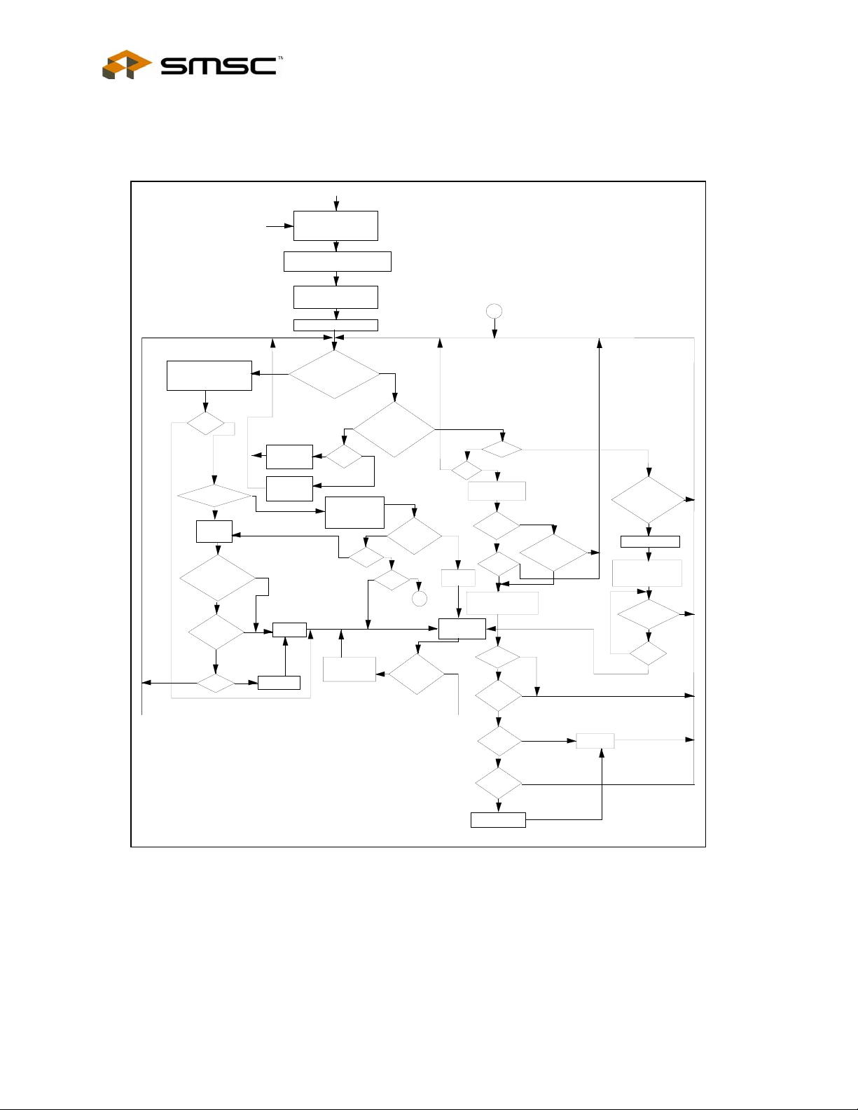
ID refers to the identification number of the ID assigned to this node.
-
NID refers to the next identification number that receives the token
after this ID passes it.
-
SID refers to the source identif i cation.
-
DID refers to the destination identification.
-
SOH refers to the start of header character; preceeds all data packets.
* Reconfig timer is programmable via setup2 register bit s 1, 0.
Note - All time values are valid for 5 Mbps.
Y
ACK? Set TMA
ACK
N
Y
Y
Set TA
YN
Free Buffer
Enquiry to
Y
Free Buffer
Increment
this ID?
N
RI?
Tran s m it
Enquiry
N
YN
ACK?
Y
NAK?
NID
FIGURE 1 - COM20020I OPERATION
Revision 12-06-06 SMSC COM20020I 3.3V
10
DATASHEET
Page 11

5Mbps ARCNET (ANSI 878.1) Controller with 2K x 8 On-Chip RAM
5.0 PROTOCOL DESCRIPTION
5.1 Network Protocol
Communication on the network is based on a token passing protocol. Establishment of the network configuration and
management of the network protocol are handled entirely by the COM20020I's internal microcoded sequencer. A
processor or intelligent peripheral transmits data by simply loading a data packet and its destination ID into the
COM20020I's internal RAM buffer, and issuing a command to enable the transmitter. When the COM20020I next
receives the token, it verifies that the receiving node is ready by first transmitting a FREE BUFFER ENQUIRY message.
If the receiving node transmits an ACKnowledge message, the data packet is transmitted followed by a 16-bit CRC. If
the receiving node cannot accept the packet (typically its receiver is inhibited), it transmits a Negative AcKnowledge
message and the transmitter passes the token. Once it has been established that the re ceiving node can accept the
packet and transmission is co mplete, the receiving node verifies the p acket. If the packet is rec eived successfully, t he
receiving node transmits an ACKnowledge message (or nothing if it is not received successfully) allowing the transmitter
to set the appropriate status bits to indicate successful or unsucce ssfu l delivery of the packet. An interrupt mask permits
the COM20020I to generate an interrupt to the processor when selected status bits become true. Figure 1 is a flow
chart illustrating the inte rn al operation of the COM20020I connected to a 20 MHz crystal oscillator.
5.2 Data Rates
The COM20020I is capable of supporting data rates from 156.25 Kbps to 5 Mbps. The following protocol description
assumes a 5 Mbps data rate. To attain the faster data rates, the clock frequency may be doubled by the internal clock
multiplier (see next section). For slower data rates, an internal clock divider scales down the clock frequency. Thus all
timeout values are scaled as shown in the following table:
Example: IDLE LINE Timeout @ 5 Mbps = 41 μs. IDLE LINE Timeout for 156.2 Kbps is 41 μs * 32 = 1.3 ms
INTERNAL
CLOCK
FREQUENCY
40 MHz Div. by 8 5 Mbps 1
20 MHz Div. by 8
Selecting Clock Frequencies Above 2.5 Mbps
To realize a 5 Mbps network, an external 40 MHz clock mus t be input. H owever, since 40 MHz is near t he frequenc y
of FM radio band, it is not practical for use for noise emission reasons. Therefore, higher frequency clocks are
generated from the 20 MHz crystal as selected through two bits in the Setup2 register, CKUP[1,0] as shown below.
The selected clock is supplied to the ARCNET controller.
CKUP1 CKUP0 CLOCK FREQUENCY (DATA RATE)
0 0 20 MHz (Up to 2.5Mbps) Default (Bypass)
0 1 40 MHz (Up to 5Mbps)
1 0 Reserved
1 1 Reserved
This clock multiplier is powered-down (bypassed) on default. After changing the CKUP1 and CKUP0 bits, the
ARCNET core operation is stopped and the internal P LL in the clock ge nerator is awakened an d it starts to generate
the 40 MHz. The lock out time of the internal PLL is 8uSec t ypically. After more than 8 μsec (this wait time is defined
as 1 msec in this data sheet), it is necessary to write c ommand data '18H' to the command register to re-start the
ARCNET core operation. This clock generator is called “clock multiplier”.
Changing the CKUP1 and CKUP0 bits must be one time or less after releasing hardware reset.
CLOCK
PRESCALER
Div. by 16
Div. by 32
Div. by 64
Div. by 128
DATA RATE
2.5 Mbps
1.25 Mbps
625 Kbps
312.5 Kbps
156.25 Kbps
TIMEOUT SCALING
FACTOR (MULTIPLY BY)
2
4
8
16
32
SMSC COM20020I 3.3V Page 11 Revision 12-06-06
DATASHEET
Page 12

5Mbps ARCNET (ANSI 878.1) Controller with 2K x 8 On-Chip RAM
The EF bit in the SETUP2 register must be set when the data rate is over 5 Mbps.
5.3 Network Reconfiguration
A significant advantage of the COM20020I is its ability to adapt to ch anges on the n etwork. Whenever a new node is
activated or deactivated, a NETWORK RECONFIGURATION is perform ed. When a new COM20020I is turned on
(creating a new active node on the network), or if the COM20020I has not received an INVITATION TO TRANSMIT
for 420mS, or if a software reset occurs, the COM20020I causes a NETWORK RECONFIGURATION by sending a
RECONFIGURE BURST consisting of eight marks and one space repeated 765 tim es. The pur pose of this burst is to
terminate all activity on the network. Since this burst is longer than any other type of transmission, the burst will
interfere with the next INVITATION TO TRANSMIT, destroy the token and keep any other node from assuming
control of the line.
When any COM20020I senses an idle line for greater than 41 μS, which occurs only when the token Is lost, each
COM20020I starts an internal timeout equal to 73μs times t he quantit y 255 minus its own ID. The CO M20020I starts
network reconfiguration by sending an invitation to transm it first to itself and then to all ot her nodes by decrementing
the destination Node ID. If the timeout expires with no line activity, the COM20020I star ts sending INVITATION TO
TRANSMIT with the Destination ID (DID) equal to the currently stored NID. Within a given network, only one
COM20020I will timeout (the one with the highest ID number). After sending the INVITATION TO TRANSMIT, the
COM20020I waits for activity on the line. If there is no activity for 37.4μS, the COM20020I increments the NID value
and transmits another INVITATION TO TRANSMIT using the NID equal to the DID. If activity appears before the
37.4μS timeout expires, the COM20020I releases control of the line. During NETWORK RECONFIGURATION,
INVITATIONS TO TRANSMIT are sent to all NIDs (1-255).
Each COM20020I on the network will finally have saved a NID value equal to the ID of the COM20020I that it
released control to. At this point, control is passed directly from o ne node to the next with no wasted INVIT ATIONS
TO TRANSMIT being sent to ID's not on the network, until the ne xt NETWORK RECONFIGURATION occurs. When
a node is powered off, the previous node attempts to pass the token to it by issuing an INVITATION TO TRANSMIT.
Since this node does not respond, the previ ous node tim es out an d transmits another IN VITAT ION TO T RANSMIT to
an incremented ID and eventually a response will be received.
The NETWORK RECONFIGURATION time depends on the number of nodes in the net work, the propagation delay
between nodes, and the highest ID number on the network, but is typically within the range of 12 to 30.5 mS.
5.4 Broadcast Messages
Broadcasting gives a particular node the ability to transmit a data packet to all n odes on the net work simultaneously.
ID zero is reserved for this feature and no node on the network can be a ssigned ID zero. To broadcast a message,
the transmitting node's processor simply loads the RAM buffer with the data packet and sets the DID equal to zero.
Figure 4 illustrates the position of each byte in the packet with the DID residing at address 0X01 or
Hex of the current page selected in the "Enable T ransmit from Page fnn" command. Each individual node has the
ability to ignore broadcast messages by setting the most significa nt bit of th e "Enab le Rec eive to Pa ge fn n" comm and
to a logic "0".
5.5 Extended Timeout Function
There are three timeouts associated with the COM20020I operation. The values of these timeouts are
controlled by bits 3 and 4 of the Configuration Register and bit 5 of the Setup 1 Register.
Response Time
The Response Time determines the maximum propagation delay allowed between any two nodes, and should be
chosen to be larger than the round trip propagation delay between the two furthest nodes on the network plus the
maximum turn around time (the time it takes a particular COM20020I to start sending a message in response to a
received message) which is a pproximately 6.4 μS. The round trip propagation delay is a function of the transmission
media and network topology. For a typical system using RG62 coax in a baseband system, a one way cable
propagation delay of 15.5 μS translates to a distance of about 2 miles. The flow chart in Figure 1 uses a value of 37.4
S (15.5 + 15.5 + 6.4) to determine if any node w ill re spond.
Revision 12-06-06 SMSC COM20020I 3.3V
12
DATASHEET
Page 13

5Mbps ARCNET (ANSI 878.1) Controller with 2K x 8 On-Chip RAM
Idle Time
The Idle Time is associated wit h a NETWORK RECONFIGURATION. Figure 1 illustrates that during a NETWORK
RECONFIGURATION one node will continually transmit INVITATIONS TO TRANSMIT until it encounters an active
node. All other nodes on the network must distinguish between this operation and an entirely idle line. During
NETWORK RECONFIGURATION, activity will appear on the line every 41 μS. This 41 μS is equal to the Response
Time of 37.4 μS plus the time it takes the COM20020I to start retransmitting another message (usually another
INVITATION TO TRANSMIT).
Reconfiguration Time
If any node does not receive the token within the Reconfiguration Time, the node will initiate a NETWORK
RECONFIGURATION. The ET 2 and ET1 bits of the Configuration Register allow the network to operate over longer
distances than the 2 miles stated earlier. The logic levels on these bits control the maximum distances over which the
COM20020I can operate by controlling the three timeout values described above. For proper network operation, all
COM20020I's connected to the same network must have the same Response Time, Idle Time, and Reconfiguration
Time.
5.6 Line Protocol
The ARCNET line protocol is considered isochronous because each byte is preceded by a start interval and ended with
a stop interval. Unlike asynchronous protocols, there is a constant amount of time separating each data byte. On a 5
Mbps network, each byte takes exactly 11 clock intervals of 200ns each. As a result, one byte is transmitted every 2.2
S and the time to transmit a mes sag e ca n be pre cise ly d eterm ine d. The line i dles i n a sp acing ( log ic " 0") co ndit ion. A
logic "0" is defined as no line activity and a logic "1" is defined as a negative pulse of 100nS duration. A transmission
starts with an ALERT BURST consisting of 6 un it intervals of mark (logic "1"). Eight bit data characters are then sent,
with each character preceded by 2 unit intervals of mark and one unit interval of space. Five types of transmission can
be performed as described below:
Invitations To Transmit
An Invitation To Transmit is used to pass the token from one node to another and is sent by the following sequence:
An ALERT BURST
An EOT (End Of Transmission: ASCII code 04H)
Two (repeated) DID (Destination ID ) ch aracters
ALERT
BURST
Free Buffer Enquiries
A Free Buffer Enquiry is used to ask another node if it is able to accept a packet of data. It is sent by the following
sequence:
An ALERT BURST
An ENQ (ENQuiry: ASCII code 85H)
Two (repeated) DID (Destination ID ) ch aracters
ALERT
BURST
Data Packets
A Data Packet consists of the actual data being sent to another node. It is sent by the following sequence:
An ALERT BURST
An SOH (Start Of Header--ASCII code 01H)
An SID (Source ID) character
Two (repeated) DID (Destination ID ) ch aracters
A single COUNT chara cter which is the 2's complement of t he number of data bytes to follo w if a short packet is
sent, or 00H followed by a COUNT character if a long packet is sent.
N data bytes where COUNT = 256-N (or 512-N for a long packet)
EOT DID DID
ENQ DID DID
SMSC COM20020I 3.3V Page 13 Revision 12-06-06
DATASHEET
Page 14

5Mbps ARCNET (ANSI 878.1) Controller with 2K x 8 On-Chip RAM
Two CRC (Cyclic Redundancy Check) charac te rs. The CRC polynomial used is: X16 + X15 + X2 + 1.
Acknowledgements
An Acknowledgement is used to acknowledge reception of a packet or as an affirmative response to FREE BUFFER
ENQUIRIES and is sent by the following sequence:
An ALERT BURST
An ACK (ACKnowledgement--ASCII code 86H) charac te r
ALERT BURST ACK
Negative Acknowledgements
A Negative Acknowledgement is used as a negative response to FREE BUFFER ENQUIRIES and is sent by the
following sequence:
An ALERT BURST
A NAK (Negative Acknowledgement--ASCII code 15H) character
ALERT BURST NAK
Revision 12-06-06 SMSC COM20020I 3.3V
14
DATASHEET
Page 15

5Mbps ARCNET (ANSI 878.1) Controller with 2K x 8 On-Chip RAM
6.0 SYSTEM DESCRIPTION
6.1 Microcontroller Interface
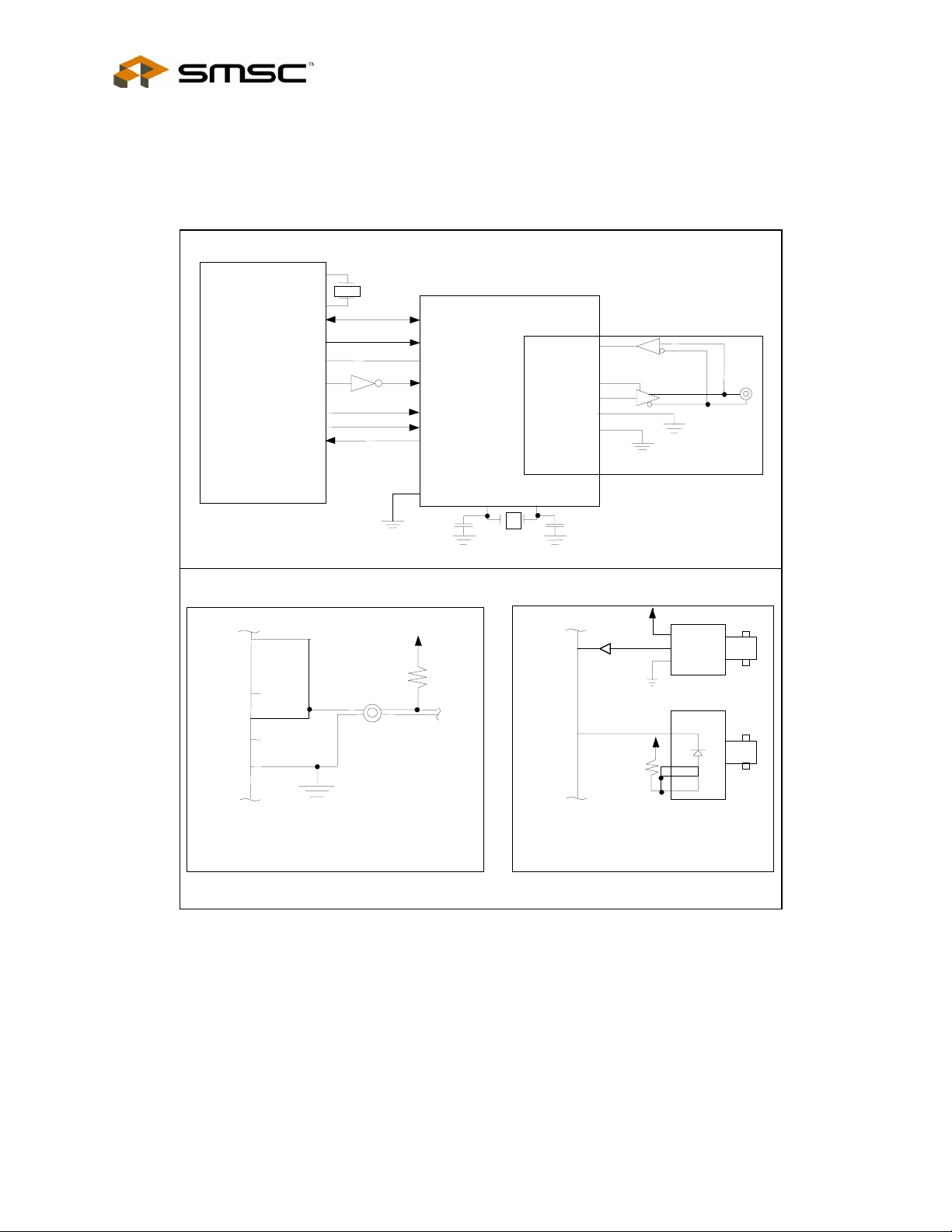
The top halves of Fig ur e 2 and Fig ure 3 illustrate typi cal COM20020I in terfaces to t he microcontr ollers. The int erfaces
consist of a 8-bit data bus, an address bus and a control bus. In order to support a wide range of microcontrollers without
requiring glue logic and without increasing the number of pins, the COM20020I automatically detects and adapts to the
type of microcontroller being used. Upon hardware reset, the COM20020I first determines whether the read and write
control signals are separate READ and WRITE signals (like the 80XX) or DIRECTION and DATA STROBE (like the
68XX). To determine the type of control signals, the device requires the software to execute at least one write access to
external memory before attemp ting t o ac cess t h e COM 200 2 0I . The device defaults to 80XX-like signals. Once the type
of control signals are determined, the COM20020I remains in this interface mode until the next hardware reset occurs.
The second determination the COM20020I makes is whether the bus is multiplexed or non-multiplexed. To determine
the type of bus, the device requires the software to write to an odd memory location followed by a read from an odd
location before attempting to access the COM20020I. The signal on the A0 pin during the odd location access tells the
COM20020I the type of bus. Since multiplexed operation requires A0 to be active low, activity on the A0 line tells the
COM20020I that the bus is non-multiplexed. The device defaults to multiplexed operation. Both determinations may be
made simultaneously by performing a WRITE followed by a READ operation to an odd location within the COM20020I
Address space 20020D registers. Once the type of bus is determined, the COM20020I remains in this interface mode
until hardware reset occurs.
Whenever nCS and nRD are activated, the preset determinations are assumed as final and will not be changed until
hardware reset. Refer to DESCRIPTION OF PIN FUNCTIONS FOR TQFP section for details on t h e related signals. All
accesses to the internal RAM and th e in ternal registers are controlled by the COM20020I. The internal RAM is accessed
via a pointer-based scheme (refer to the Sequential Access Memory section), and the internal registe rs are accessed via
direct addressing. Many peripherals are not fast enough to take advantage of high-speed microcontrollers. Since
microcontrollers do not typically have READY inputs, standard peripherals cannot extend cycles to extend the access
time. The access time of the COM20020I, on the other hand, is so fast that it does not need to limit the speed of the
microcontroller. The COM20020I is designed to be flexi ble so that it is independent of the microcontrol ler speed.
The COM20020I provides for no wait state arbit ration via direct address ing to its internal registers an d a pointer based
addressing scheme to access its internal RAM. The pointer may be used in auto-increment mode for typical sequential
buffer emptying or loading, or it can be taken out of auto-increment mode to perform random accesses to the RAM. The
data within the RAM is accessed through the data register. Data being read is prefetched from memory and placed into
the data register for the microc ontroller to read. It is important to notice that only by writing a new address pointer
(writing to an address pointer low), one obtains the contents of COM20020I internal RAM. Performing only read from the
Data Register does not load new data from the internal RAM. During a write operation, th e data is stored in the data
register and then written into memory. Whenever the pointer is loaded for reads with a new value, data is immediately
prefetched to prepare for the first read operation .
SMSC COM20020I 3.3V Page 15 Revision 12-06-06
DATASHEET
Page 16
5Mbps ARCNET (ANSI 878.1) Controller with 2K x 8 On-Chip RAM
A
A15A
A
A
A
D0-AD2, D32/BAL
XTAL1
0/nMU
COM20020I
20 MHz
XTAL
XTAL2
RXIN
nTXEN
nPULSE
nPULSE
GND
27 pF
LTC1480 or
Equiv.
Differential
Configuratio
Media
*
may be
with Figure A, B or
8051
XTAL1
XTAL2
D0-
RESET
nWR
nINT1
LE
nRD
nCS
nRESET
nRD/nD
nWR/DI
nINTR
27 pF
RXIN
TXEN
nPULSE
nPULSE
GND
BACKPLANE
FIGURE A
+3.3V
100
RXIN
nPULSE
NOTE: COM20020 must be in backplane mode
3.3V-5V Converter
FIGURE B
+5V
+5V
2
6
HFD3212-
7
Transmitte
HFE4211-
3
2
6
7
2 Fiber
(ST
Receive
FIGURE 2 - MULTIPLEXED, 8051-LIKE BUS INTERFACE WITH RS-485 INTERFACE
Revision 12-06-06 SMSC COM20020I 3.3V
16
DATASHEET
Page 17
5Mbps ARCNET (ANSI 878.1) Controller with 2K x 8 On-Chip RAM
A
A
X
A
A1A
A
A
XTAL1
XTAL2
6801
D0-D7
nRES
nIOS
R/nW
nIRQ1
0
1
2
7
RXIN
nTXEN
nPULSE1
nPULSE2
GND
3.3V-5V Converter
N/C
D0-D7
nCS
nRESET
nRD/nDS
nWR/nDIR
nINTR
27 pF
HYC9068 or
HYC9088
RXIN
nPULSE1
nPULSE2
17, 19,
4, 13, 14
0.47
uF
FIGURE 3 - NON-MULTIPLEXED, 6801-LIKE BUS INTERFACE WITH RS-485 INTERFACE
0/nMU
2/BALE
FIGURE C
COM2002
XTAL1
20MHz
XTAL
+5V
6
3
+
10
uF
nPULSE1
nPULSE2
XTAL2
+
10
uF
12
11
5.6K
1/2W
5.6K
1/2W
Traditional Hybrid
-5V
*Valid for 2.5 Mbps only.
RXIN
TXEN
GND
Differential Driver
27 pF
0.47
uF
Configuration
LTC1480 or
Equiv.
Configuration
Media Interface
*
may be replaced
with Figure A, B or C.
0.01 uF
1KV
SMSC COM20020I 3.3V Page 17 Revision 12-06-06
DATASHEET
Page 18
5Mbps ARCNET (ANSI 878.1) Controller with 2K x 8 On-Chip RAM
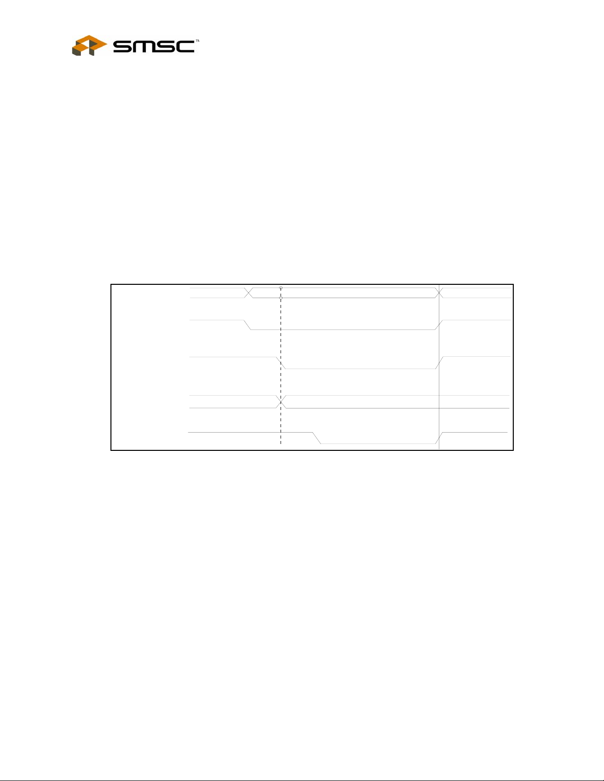
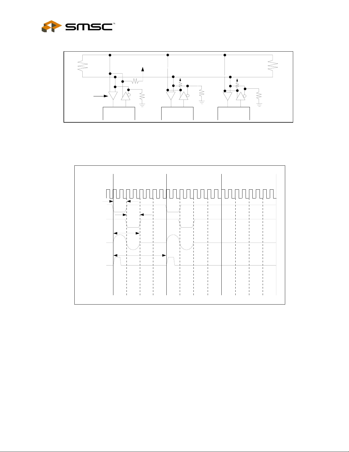
High Speed CPU Bus Timing Support
High speed CPU bus support was added to the COM20020I. The reasoning behind this is as follows: With the Host
interface in Non-multiplexed Bus mode, I/O address and Chip Select signals must be stable before the read signal is
active and remain after the read signal is inactive. But the High Speed CPU bus timing doesn't adhere to these
timings. For example, a RISC type single chip microcontroller (like the HITACHI SuperH series) changes I/O addres s
at the same time as the read signal. Therefore, several external logic ICs would be required to connect to this
microcontroller.
In addition, the Diagnostic Status (DIAG) register is cleared automatically by reading itself . T he internal DIAG register
read signal is generated by decoding the Address (A2-A0), Chip Select (nCS) and Rea d (nRD) signals. T he decoder
will generate a noise spike at the above ti ght timing. The DI AG register is cleared by the spike signal without r eading
itself. This is unexpected operation. Reading the internal RAM an d Next Id Register have the same mechanism as
reading the DIAG register.
Therefore, the address decode and host interface mode blocks were modified to fit the above CPU interface to
support high speed CPU bus timing. In Intel CPU mode (nRD, nWR mode), 3 bit I/O address (A2-A0) and Chi p
Select (nCS) are sampled internally by Flip- Flops on the falling edge of the internal delayed nRD signa l. The internal
real read signal is the more delayed nRD signal. But the rising edge of nRD doesn't delay. By this modification, the
internal real address and Chip Select are stable while the internal real read signal is active. Refer to Figure 4 below.
A2-A0, nCS
nRD
Delayed nRD
(nRD1)
Sampled A2-A0, nCS
More delayed nRD
(nRD2)
VALID
VALID
FIGURE 4 - HIGH SPEED CPU BUS TIMING - INTEL CPU MODE
The I/O address and Chip Select signals, which are supplied to the data output logic, are not sampled. Also, the nRD
signal is not delayed, because the above sampling and delaying paths decrease the data access time of the read
cycle.
The above sampling and delaying signals are supplied to the Read Pulse Generation logic which generates the
clearing pulse for the Diagnostic register and generates the starting pulse of the RAM Arbitration. T ypical delay time
between nRD and nRD1 is around 15nS and between nRD1 and nRD2 is around 10nS.
Longer pulse widths are needed due to these d elays on nRD signal. However, the CP U can insert some wait cycles
to extend the width without any impact on performance.
The RBUSTMG bit was added to Disable/Enable the High Speed CPU Read function. It is defined as: RBUSTMG= 0,
Disabled (Default); RBUSTMG=1, Enabled.
Revision 12-06-06 SMSC COM20020I 3.3V
18
DATASHEET
Page 19

5Mbps ARCNET (ANSI 878.1) Controller with 2K x 8 On-Chip RAM
In the MOTOROLA CPU mode (DIR, nDS mode), the same modifications apply.
RBUSTMG BIT BUS TIMING MODE
0 Normal Speed CPU Read and Write
1 High Speed CPU Read and Normal Speed CPU Write
6.2 Transmission Media Interface
The bottom halves of Figure 2 and Figure 3 illustrate the COM20020I interface to the transmission medi a used to
connect the node to the network. TABLE 1 - TYPICAL MEDIA lists different types of cable which are suitable for
ARCNET applications. The user may interface to the cable of choice in one of three ways:
Traditional Hybrid Interface
The Traditional Hybrid Interface is that which is used with previous ARCNET devices. The Hybrid Interface is
recommended if the node is to be placed in a network with other Hybrid-Interfaced nodes. The Traditional Hybrid
Interface is for use with nodes operating at 2.5 Mbps only. The transformer co upling of the Hybrid offers isolation for the
safety of the system and offers high Common Mode Rejection. The Traditional Hybrid Interface uses circuits like
SMSC's HYC9068 or HYC9088 to transfer the pulse-encoded data between the cable and the COM20020I. The
COM20020I transmits a logic "1" by generating two 100nS non-overlapping negative pulses, nPULSE1 and nPULSE2.
Lack of pulses indicates a logic "0". T he nPU LSE 1 and nP UL SE2 sig nals ar e sent t o the H ybrid, whic h creat es a 20 0nS
dipulse signal on the media.
A logic "0" is transmitted by the absence of the dipulse. During reception, the 200nS dipulse appearing on the media is
coupled through the RF transformer of the LAN Driver, which produces a positive pulse at the RXIN pin of the
COM20020I. The pulse on the RXIN pin represents a logic "1". Lack of pulse represents a logic "0". Typically, RXIN
pulses occur at multiples of 400nS. The COM20020I can tolerate distortion of plus or minus 100nS and still correctly
capture and convert the R XIN pulses to NRZ format. Figure 5 illustrates th e events which occur in transmission or
reception of data consisting of 1, 1, 0.
Please refer to TN7-5 – Cabling Guidelines for the COM20020I ULANC, available from SMSC, for recommended
cabling distance, termination, and node count for ARCNET nodes.
Backplane Configuration
The Backplane Open Drain Configuration is recommended for cost-sensitive, short-distance applications like backplanes
and instrumentation. This mode is advantageous because it saves components, cost, and power.
Since the Backplane Configurati on encodes data differe ntly than the tradit ional Hybrid Conf iguration, no des utilizing th e
Backplane Configuration cannot communicate directly with nodes utilizing the Traditional Hybrid Configuration. The
Backplane Configuration does not isolate the node from the media nor protects it from Common Mode noise, but
Common Mode Noise is less of a p roblem in short distances.
The COM20020I supplies a programmable output driver for Backplane Mode operation. A push/pull or open drain driver
can be selected by programming the P1MODE bit of the Setup 1 Register (see register descriptions for details). The
COM20020I defaults to an open drain output.
The Backplane Configuration provides for direct connection between the COM20020I and the media. Only one pull-up
resistor (in open drain configuration of the output driver) is required somewhere on the media (not on each individual
node). The nPULSE1 signal, in this mode, is an open drain or push/pull driver and is used to directly drive the media. It
issues a 200nS negative pulse to transmit a logic "1". Note that when used in the open-drain mode, the COM20020I
does not have a fail/safe input on the RXIN pin. The nPULSE1 signal actually contains a weak pull-up resistor. This
pull-up should not take the place of the resistor required on the me dia for open drain mode .
SMSC COM20020I 3.3V Page 19 Revision 12-06-06
DATASHEET
Page 20
5Mbps ARCNET (ANSI 878.1) Controller with 2K x 8 On-Chip RAM
RT RT
+3.3V
LTC1480 or
Equiv.
RBIAS
+3.3V
RBIAS
+3.3V
RBIAS
COM2002
COM2002 COM2002
FIGURE 5 - COM20020I NETWORK USING RS-485 DIFFERENTIAL TRANSCEIVERS
20MHZ
CLOCK
(FOR REF.
ONL Y)
nPULSE1
100ns
nPULSE2
10
100ns
200ns
1
DIPULSE
400ns
RXIN
FIGURE 6 - DIPULSE WAVEFORM FOR DATA OF 1-1-0
Revision 12-06-06 SMSC COM20020I 3.3V
20
DATASHEET
Page 21

5Mbps ARCNET (ANSI 878.1) Controller with 2K x 8 On-Chip RAM
In typical applications, the serial backplane is terminated at both ends and a bias is provided by the external pull-up
resistor.
The RXIN signal is directly connected to the cable via an internal Schmitt trigger. A negative pulse on this input
indicates a logic "1". Lack of pulse indicates a logic "0". For typical single-ended backplane applications, RXIN is
connected to nPULSE1 to make the serial backplane data line. A ground line (from the coax or twisted pair) should run
in parallel with the signal. For applications requiring different treatment of the receive signal (like filtering or squelching),
nPULSE1 and RXIN remain as independent pins. External differential drivers/receivers for increased range and common
mode noise rejection, for example, would requ ire the si gnals to be inde pende nt of one another.
When the device is in Backplane Mode, the clock provided by the nPULSE2 signal may be used for encoding the data
into a different encoding scheme or other synchronous operations needed on th e serial data stream.
Differential Driver Configuration
The Differential Driver Configuration is a special case of the Backplane Mode. It is a dc coupled configuration
recommended for applications like car-area networks or other cost-sensitive applications which do not require direct
compatibility with existing ARCNET nodes and do not requi re isola tion.
The Differential Driver Configuration cannot communicate directly with nodes utilizing the Traditional Hybrid
Configuration. Like the Backpla ne Conf igur atio n, the Differ e ntia l Driv er Conf ig urati on does n ot isol ate t he node fr om th e
media.
The Differential Driver interface includes a RS485 Driver/Receiver to transfer the data between the cable and the
COM20020I. The nPULSE1 signal transmits the data, provided the Transmit Enable signal is active. The nPULSE1
signal issues a 200nS (at 2.5Mbps) negative pulse to transmit a logic "1". Lack of pulse indicates a logic "0". The RXIN
signal receives the data, the transmitter portion of the COM20020I is disabled during reset and the nPULSE1, nPULSE2
and nTXEN pins are inactive.
Programmable TXEN Polarity
To accommodate transceivers with active high ENABLE pins, the COM20020I contains a programmable TXEN output.
To program the TXEN pin for an active high pulse, the nPULSE2 pin should be connected to ground. To retain the
normal active low polarity, nPULSE2 should be left open. The polarity determination is made at power on reset and is
valid only for Backplane Mode operation. The nPULSE2 pin should remain grounded at all times if an active high
polarity is desired.
SMSC COM20020I 3.3V Page 21 Revision 12-06-06
DATASHEET
Page 22

5Mbps ARCNET (ANSI 878.1) Controller with 2K x 8 On-Chip RAM
A
0
/
n
M
U
A
A
2
/
B
A
L
E
AD0-AD2,
D3-D7
nINTR
nRESET
nRD/nDS
nWR/DIR
nCS
X
1
ADDRESS
DECODING
CIRCUITRY
2K x 8
RAM
ADDITIONAL
REGISTERS
STAT US/
COMMAND
REGISTER
RESET
LOGIC
MICRO-
SEQUENCER
AND
WORKING
REGISTERS
TX/RX
LOGIC
nPULSE1
nPULSE2
nTXEN
RXIN
XTAL1
OSCILLA TOR
XTAL2
BUS
ARBITRATION
CIRCUITRY
RECONFIGURATION
TIMER
FIGURE 7 - INTERNAL BLOCK DIAGRAM
NODE ID
LOGIC
Revision 12-06-06 SMSC COM20020I 3.3V
22
DATASHEET
Page 23

5Mbps ARCNET (ANSI 878.1) Controller with 2K x 8 On-Chip RAM
Table 1 - Typical Media
CABLE TYPE
RG-62 Belden #86262
RG-59/U Belden #89108
RG-11/U Belden #89108
IBM Type 1* Belden #89688
IBM Type 3* Telephone Twisted
Pair Belden #1155A
COMCODE 26 AWG Twisted
Pair Part #105-064-703
*Non-plenum-rated cables o f this type are also available.
Note: For more detailed information on Cabling options including RS-485, transformer-coupled RS-485 and Fiber Optic
interfaces, please refer to TN7-5 – Cabling Guidelines for the COM20020I ULANC, available from Standard
Microsystems Corporation.
NOMINAL
IMPEDANCE
93Ω
75Ω
75Ω
150Ω
100Ω
105Ω
ATTENUATION PER 1000 FT.
AT 5 MHz
5.5dB
7.0dB
5.5dB
7.0dB
17.9dB
16.0dB
SMSC COM20020I 3.3V Page 23 Revision 12-06-06
DATASHEET
Page 24

5Mbps ARCNET (ANSI 878.1) Controller with 2K x 8 On-Chip RAM
7.0 FUNCTIONAL DESCRIPTION
7.1 Microsequencer
The COM20020I contains an internal microsequenc er which pe rforms all of the control o perations nece ssary to carry
out the ARCNET protocol. It consists of a clock generator, a 544 x 8 ROM, a program counter, two instruction
registers, an instruction decoder, a no-op generator, jump logic, and reconfiguration logic.
The COM20020I derives a 10 MHz and a 5 MHz clock from the output clock of the Clock Multiplier. These clock s
provide the rate at which the instructions are executed within the COM20020I. The 10 MHz clock is the rate at which
the program counter operates, while the 5 MHz clock is the rate at which the instructions are executed. The
microprogram is stored in the ROM and the instructions are fetched and then placed into the instruction registers.
One register holds the opcode, while the other holds the immediate data. Once the instruction is fetched, it is
decoded by the internal instruction decoder, at which point the COM20020I proceeds to execute the instruction.
When a no-op instruction is encountered, the microsequencer enters a timed loop and the program counter is
temporarily stopped until the loop is complete. When a jump instruction is encountered, the program counter is
loaded with the jump address from the ROM. The COM20020I contains an internal reconfiguration timer which
interrupts the microsequencer if it has timed out. At this point the program counter is cl eared and the MYRECON bit
of the Diagnostic Status Register is set.
Table 2 - Read Register Summary
REGISTER
STATUS
DIAG.
STATUS
ADDRESS
PTR HIGH
ADDRESS
PTR LOW
DATA
SUB ADR
CONFIG-
URATION
TENTID
NODE ID
SETUP1
NEXT ID
SETUP2
Note*: (R/W) This bit can be Written or Read. For more information see Appendix B.
MSB
RI/TRI X/RI X/TA POR TEST RECON TMA TA/
MY-RECON DUPID
RD-DATA
A7 A6 A5 A4 A3 A2 A1 A0
D7 D6 D5 D4 D3 D2 D1 D0
(R/W)* 0 0 0 (R/W)*
RESET
TID7 TID6 TID5 TID4 TID3 TID2 TID1 TID0
NID7 NID6 NID5 NID4 NID3 NID2 NID1 NID0
P1 MODE FOUR
NXT ID7
RBUS-TMG X
AUTO-
INC
CCHE
N
NAKS
NXT
ID6
RCV-
ACT
X X X A10 A9 A8
TXEN ET1 ET2
X
NXT
ID5
CKU
P1
READ
TOKEN
RCV-
ALL
NXT
ID4
CKUP0 EF
EXC-
NAK
CKP3 CKP2 CKP1
NXT
ID3
TENTID NEW
NEXT
ID
SUB-
AD2
BACKPLANE
NXT
ID2
NO-
SYNC
SUB-
AD1
SUB-
AD1
NXT
ID1
RCN-
TM1
LSB ADDR
TTA
X
SUB-
AD0
SUB-
AD0
SLOW-
ARB
NXT
ID0
RCM-
TM2
00
01
02
03
04
05
06
07-0
07-1
07-2
07-3
07-4
Revision 12-06-06 SMSC COM20020I 3.3V
24
DATASHEET
Page 25

5Mbps ARCNET (ANSI 878.1) Controller with 2K x 8 On-Chip RAM
Table 3 - Write Register Summary
ADDR MSB
00
01
02
03
04
05
06
07-0
07-1
07-2
07-3
07-4
Note*: (R/W) This bit can be Written or Read. For more information see Appendix B.
RI/TR1 0 0 0 EXCNAK
C7 C6 C5 C4 C3 C2 C1 C0
RD-
DATA
A7 A6 A5 A4 A3 A2 A1 A0
D7 D6 D5 D4 D3 D2 D1 D0
(R/W)* 0 0 0 (R/W)*
RESE
T
TID7 TID6 TID5 TID4 TID3 TID2 TID1 TID0
NID7 NID6 NID5 NID4 NID3 NID2 NID1 NID0
P1-
MODE
0 0 0 0 0 0 0 0
RBUS-
TMG
AUTO-
INC
CCHEN TXEN ET1 ET2 BACK-
FOUR
NAKS
0
0 0 0 A10 A9 A8
0 RCV-
CKUP
1
WRITE
RECO
N
SUB-
AD2
PLANE
CKP3 CKP2 CKP1
ALL
CKUP0 EF NO-
SYNC
NEW
NEXTID
SUB-
AD1
SUB-
AD1
RCN-
TM1
LSB REGISTER
TA/
TTA
SUB-
AD0
SUB-
AD0
SLOW-
ARB
RCN-
TM0
INTERRUPT
MASK
COMMAND
ADDRESS
PTR HIGH
ADDRESS
PTR LOW
DATA
SUBADR
CONFIG-
URATION
TENTID
NODEID
SETUP1
TEST
SETUP2
7.2 INTERNAL REGISTERS
The COM20020I contains 14 internal registers. TABLE 2 and TABLE 3 illustrate the COM20020I register map. All
undefined bits are read a s undefined and must be written as logic "0".
Interrupt Mask Register (IMR)
The COM20020I is capable of generating an interrupt signal when certain status bits become true. A write to the IMR
specifies which status bits will be enabled to generate an interrupt. The bit positions in the IMR are in the same position
as their corresponding status bits in the Status Register and Diagnostic Status Register. A logic "1" in a particular
position enables the corresponding interrupt. The Status bits capable of generating an interrupt include the Receiver
Inhibited bit, New Next ID bit, E xcessive NAK bit, Reconfiguration Timer bit, and Transmitt er Available bit. No other
Status or Diagnostic Status bits can generate an interrupt.
The six maskable status bits are ANDed with their respective mask bits, and the results are ORed to produce the
interrupt signal. An RI or TA interrupt is masked when the corresponding mask bit is reset to logic "0", but will reappear
when the corresponding mask bit is set to logic "1" again, unless the interrupt status condition has been cleared by this
time. A RECON interrupt is cleared when the "Clear Flags" command is issued. An EXCNAK interrupt is cleared when
the "POR Clear Flags" command is issued. A New Next ID interrupt is cleared by reading the Next ID Register. The
Interrupt Mask Register defaults to the value 0000 0000 upon hardware reset.
Data Register
This read/write 8-bit regist er is used as the channel thr ough which the data to and fr om the RAM passes. The data is
placed in or retrieved from the address location presently specified by the address pointer. The contents of the Data
Register are undefined upon hardware reset. In case of READ operation, the Data Register is loaded with the contents
of COM20020I Internal Memory upon writing Address Pointer low only once.
Tentative ID Register
The Tentative ID Register is a read/write 8-bit register accessed when the Sub Address Bits are set up accordingly
(please refer to the Configurat ion Register and SUB ADR Register). The Te ntative ID Register can be used while the
SMSC COM20020I 3.3V Page 25 Revision 12-06-06
DATASHEET
Page 26

5Mbps ARCNET (ANSI 878.1) Controller with 2K x 8 On-Chip RAM
node is on-line to build a network map of those nodes existing on the network. It minimizes the need for operator
interaction with the network. The node determines the existence of other nodes by placing a Node ID value in the
Tentative ID Register a nd waiting to see if the Tentative I D bit of the Diagnostic Status Register gets set. The network
map developed by this method is only valid for a short period of time, since nodes may join or depart from the network at
any time. When using the Tentative ID feature, a node cannot detect the existence of the next logical node to which it
passes the token. The Next ID Register will hold the ID value of that node. The Tentative ID Register defaults to the
value 0000 0000 upon hardware reset only.
Node ID Register
The Node ID Register is a read/write 8-bit register accessed when the Sub Address Bits are set up accordingly (please
refer to the Configuratio n Register and SUB ADR Register). The Node I D Register contains the unique value which
identifies this particular n ode. Each nod e on the net work must have a u nique Node I D value at all times. The D uplicat e
ID bit of the Diagnostic Status Register helps the use r find a unique Node ID. Refer to the Initialization Sequence section
for further detail on the use of the DUPID bit. The core of the COM20020I does not wake up until a Node ID other than
zero is written into the Node ID Register. During this time, no microcode is executed, no tokens are passed by this node,
and no reconfigurations are caused by this node. Once a non-zero NodeID is placed into the Node ID Register, the core
wakes up but will not join the network until the TXEN bit of the Configuration Register is set. While the Transmitter is
disabled, the Receiver portion of the device is still functional and will provide the user with useful information about the
network. The Node ID Register defaults to the va lue 0000 0000 upon hardw a re reset only.
Next ID Register
The Next ID Register is an 8- bit, read- only regist er, access ed when the sub-address bits are set up accordingly (please
refer to the Configuration Register and SUB ADR Register). The Next ID Register holds the value of the Node ID to
which the COM20020I will pass the token. When used in conjunction with the Tentative ID Register, the Next ID
Register can provide a com plete network map. The Next ID Re gister is updated each time a no de enters/leaves the
network or when a network reconfiguration occurs. Each time the microsequencer updates the Next ID Register, a New
Next ID interrupt is generated. This bit is cleared by reading the Next ID Register. Default value is 0000 0000 upon
hardware or software reset.
Status Register
The COM20020I Status Register is an 8-bit read-only register. All of the bits, except for bits 5 and 6, are software
compatible with previous SMSC ARCNET devices. In previous SMSC ARCNET devices the Extended Timeout status
was provided in bits 5 and 6 of the Status Register. In the COM20020I, the COM20020I, the COM90C66, and the
COM90C165, COM20020I-5, COM20051 and COM20051+ these bits exist in and are controlled by the Configuration
Register. The Status Register contents are defined as in TABLE 4, but are defined differently during the Command
Chaining operation. Please refer to the Command Chaining section for the definition of the Status Register during
Command Chaining operation. The Status Register defaults to the value 1XX1 0001 upon either hardware or software
reset.
Diagnostic Status Register
The Diagnostic Status Register contains seven read-only bits which help the user troubleshoot the network or node
operation. Various combinations of these bits and the TXEN bit of the Configuration Register represent different
situations. All of these bits, except the Excessive NAcK bit and the New Next ID bit, are reset to logic "0" upon reading
the Diagnostic Status Register or upon software or hardware reset. The EXCNAK bit is reset by the "POR Clear Flags"
command or upon software or hardware reset. The Diagnostic Status Register defaults to the value 0000 000X upon
either hardware or softw are re se t.
Command Register
Execution of commands are initi ated by performing microc ontroller writes to this register. Any combinations of written
data other than those listed in TABLE 5 are not permitted and may result in incorrect chip and/or network ope ra tion.
Address Pointer Registers
These read/write registers ar e each 8-bits wide and are used for addressing the internal RAM. Ne w pointer addresses
should be written by first writi ng to the High Register and then writing to the Low Register becaus e writing to the Low
Register loads the address. The contents of the Address Pointer High and Low Registers are undefined upon hardware
reset. Writing to Address Pointer low loads the address.
Configuration Register
The Configuration Regist er is a read/write register which is used to c onfigure the different modes of the COM20020I.
The Configuration Register defaults to the value 0001 1000 upon hardware reset only. SUBAD0 and SUBAD1 point to
the selection in Register 7.
Revision 12-06-06 SMSC COM20020I 3.3V
26
DATASHEET
Page 27

5Mbps ARCNET (ANSI 878.1) Controller with 2K x 8 On-Chip RAM
Sub-Address Register
The sub-address register is n ew to the COM20020I, previously a re served register. Bits 2, 1 and 0 are used to select
one of the registers assi gned to addr ess 7h. S UB AD 1 an d SUBAD0 alread y exist in the Configuration register on the
COM20020IB. They are exactly same as those in the Sub-Address register. If the SUBAD1 and SUBAD0 bits in the
Configuration register are changed, the SUBAD1and SUBAD0 in the Sub-Address register are also changed.
SUBAD2 is a new sub-address bit. It Is used to access the 1 new Set Up register, SET UP2. This register is selected
by setting SUBAD2=1. The SUBAD2 bit is cleared automatically by writing the Configuration register.
Setup 1 Register
The Setup 1 Register is a read/write 8-bit register accessed when the Sub Address Bits are set up accordingly (see the
bit definitions of the Config uration Register). The Set up 1 Register allows the us er to change the network sp eed (data
rate) or the arbitration speed independently, invoke the Receive All feature and change the nPULSE1 driver type. The
data rate may be slowed to 156.25Kbps and/or the arbitration speed may be slowed by a factor of two. The Setup 1
Register defaults to the value 0000 0000 upon hardware reset only.
Setup 2 Register
The Setup 2 R egist er is new t o the CO M200 20I. I t is an 8-bit read/write register accessed when the Sub Address Bits
SUBAD[2:0] are set up according ly (see the bit definitions of the Sub Address Register). T his r egis ter cont ains bits for
various functions. The CKUP1,0 bits select the clock to be generated from the 20 MHz crystal. The RBUSTMG bit is
used to Disable/Enable Fast Read function for High Spee d CPU bus support. The EF bit is used to en able the new
timing for certain functions in the COM20020I (if EF = 0, the timing is the same as in the COM20020I Rev. B). See
Appendix “A”. The NOSYNC bit is used to enable the NOSYNC function during i nitialization. If this bit is reset, the
line has to be idle for the RAM initialization sequence to be written. If set, the line does not have to be idle for the
initialization sequence to be written. See Appendix “A”.
The RCNTM[1,0] bits are used to set the time-out period of the recon timer. Programming this timer for shorter time
periods has the benefit of shortened network reconfiguration periods. T he time periods shown in the table on the
following page are limited by a maximum number of nodes in the network. These time-out period values are for
5Mbps. For other data rates, scale the time-out period time valu es acc ordi ngly; th e m axi mum node cou nt remains th e
same.
RCNTM1 RCNTM0
0 0 420 mS Up to 255 nodes
0 1 105 mS Up to 64 nodes
1 0 52.5 mS Up to 32 nodes
1 1 26.25 mS* Up to 16 nodes*
Note*: The node ID value 255 must exist in the network for the 26.25 mS time-out to be valid.
TIME-OUT
PERIOD
MAX NODE
COUNT
SMSC COM20020I 3.3V Page 27 Revision 12-06-06
DATASHEET
Page 28

5Mbps ARCNET (ANSI 878.1) Controller with 2K x 8 On-Chip RAM
Table 4 - Status Register
BIT BIT NAME SYMBOL DESCRIPTION
7 Receiver
Inhibited
6,5 (Reserved) These bits are undefined.
4 Power On Reset POR
3 Test TEST
2 Reconfiguration RECON
1 Transmitter
Message
Acknowledged
0 Transmitter
Available
RI
TMA
TA
This bit, if high, indicate s that the receiver is not enabled because
either an "Enable Receive to Page fnn" command was never
issued, or a packet has been depo si ted into the RAM buffer page
fnn as specified by the last "Enable Receive to Page fnn"
command. No messages will be received until thi s co mmand is
issued, and once the message has been rece ived, the R I bit is set,
thereby inhibiting the receiver. The RI bit is cleared by issuing an
"Enable Receive to Page fnn" command . This bi t, when se t, w ill
cause an interrupt if the corresponding bit of the Interrupt Mask
Register (IMR) is also set. When this bit is set and another station
attempts to send a packet to thi s sta tion , thi s sta tion will se nd a
NAK.
This bit, if high, indicates that the COM20020I has been reset by
either a software reset, a hardware reset, or writing 00H to the
Node ID Register. The POR bit is cleared by the "Clear Flags"
command.
This bit is intended for test and diagnostic purposes. It is a log ic
"0" under normal operating cond i tio ns.
This bit, if high, indicates that the Line Idle Time r has ti med out
because the RXIN pin was idle for 41μS. The RECON bit is
cleared during a "Clear Flags" command. Th is bit, w hen se t, will
cause an interrupt if the corresponding bit in the IMR is also set.
The interrupt service routine should consist of examining the
MYRECON bit of the Diagnostic Status Register to determine
whether there are consecutive reconfigurations caused by this
node.
This bit, if high, indicates that the packet transmitted as a result of
an "Enable Transmit from Page fnn" command has been
acknowledged. This bit should only be consid ered val id after the
TA bit (bit 0) is set. Broadcast messages are never acknowledged.
The TMA bit is cleared by issuing the "Enable Transmit from Page
fnn" command.
This bit, if high, indicates that the transmitter is available for
transmitting. This bit is set when the last byte of scheduled pa cket
has been transmitted out, or upon execution of a "Disable
Transmitter" command. The TA bit is cleared by issuing the
"Enable Transmit from Page fnn" command after the node next
receives the token. This bit, when set, will cause an interrupt if the
corresponding bit in the IMR i s also set.
Revision 12-06-06 SMSC COM20020I 3.3V
28
DATASHEET
Page 29

5Mbps ARCNET (ANSI 878.1) Controller with 2K x 8 On-Chip RAM
Table 5 - Diagnostic Status Registe r
BIT BIT NAME SYMBOL DESCRIPTION
7
My
Reconfiguration
6 Duplicate ID DUPID
5 Receive
Activity
4 Token Seen TOKEN
3 Excessive NAK EXCNAK
2 Tentative ID TENTID
1 New Next ID NEW
1,0 (Reserved) These bits are undefined.
MYRECON
RCVACT
NXTID
This bit, if high, indicates that a past reconfigur ation was caused by
this node. It is set when the Lost Token Timer times out, and
should be typically read following an interrupt caused by RECON.
Refer to the Improved Diagnostics secti on for fu rthe r detail .
This bit, if high, indicates that the value in the Node ID Register
matches both Destination ID characters of the token and a
response to this token has occurred. Trailing zero's are also
verified. A logic "1" on this bit indicates a duplicate Node ID, thus
the user should writ e a new value int o the Node ID Regi ster. This
bit is only useful for duplicate ID detection when the device is off
line, that is, when the transmitter is disabled. When the device is
on line this bit will be set every time the device gets the token. This
bit is reset automatically upon reading the Diagnostic Status
Register. Refer to the Improved Diagnostics section for further
detail.
This bit, if high, indicates that data activity (logic "1") was detected
on the RXIN pin of the device. Refer to the Improved Diagnostics
section for further detail.
This bit, if high, indicates that a token has been seen on the
network, sent by a node other than this one. Re fer to the Improved
Diagnostic section for further detail.
This bit, if high, indicates that either 128 or 4 Negative
Acknowledgements have occurred in response to the Free Buffer
Enquiry. This bit is cleared upon the "POR Clear Flags" command.
Reading the Diagnostic Status Register does not clear this bit.
This bit, when set, will cause an interrupt if the corresponding bit in
the IMR is also set. Refer to the Improve d Diagnostics sect ion for
further detail.
This bit, if high, indicates that a response to a token whose DID
matches the value in the Tent ative ID Register has occurred. The
second DID and the tra iling zero's are not checked. Since e ach
node sees every token passed around the network, this feature
can be used with the device on-line in order to build and update a
network map. Refer to the Improved Diag nostics section for further
detail.
This bit, if high, indicates that the Next ID Register has been
updated and that a node has either joined or left the network.
Reading the Diagnostic Status Register does not clear this bit. This
bit, when set, will cause an interrupt if the corresponding bit in the
IMR is also set. The bit is cleared by reading the Next ID Register.
SMSC COM20020I 3.3V Page 29 Revision 12-06-06
DATASHEET
Page 30

5Mbps ARCNET (ANSI 878.1) Controller with 2K x 8 On-Chip RAM
Table 6 - Command Register
DATA COMMAND DESCRIPTION
0000 0000 Clear
Transmit
Interrupt
0000 0001 Disable
Transmitter
0000 0010 Disable
Receiver
b0fn n100 Enable
Receive to
Page fnn
00fn n011 Enable
Transmit from
Page fnn
0000 c101 Define
Configuration
000r p110 Clear Flags
0000 1000 Clear
Receive
Interrupt
0001 1000
Start Internal
Operation
This command is used only in the Command Chaining operation.
Please refer to the Command Chaining section for definition of
this command.
This command will cancel any pending transmit command
(transmission that has not yet started) and will set the TA
(Transmitter Available) status bit to logic "1" when the
COM20020I next receives the token.
This command will cancel any pending receive command. If the
COM20020I is not yet receiving a packet, the RI (Receiver
Inhibited) bit will be set to logic "1" the next time the token is
received. If packet reception is already underway, reception will
run to its normal conclusion.
This command allows the COM20020I to receive data packets
into RAM buffer page fnn and resets the RI status bit to logic "0".
The values placed in the "nn" bits indicate the page that the data
will be received into (page 0, 1, 2, or 3). If the v alue of "f" is a
logic "1", an offset of 256 bytes will be added to that page
specified in "nn", allowing a finer resolution of the buffer. Refer to
the Selecting RAM Page Size section for further detail. If the
value of "b" is logic "1", the device will also receive broadcasts
(transmissions to ID zero). The RI status bit is set to logic "1"
upon successful reception of a message.
This command prepares the COM20020I to begin a transmit
sequence from RAM buffer page fnn the next time it receives the
token. The values of the "nn" bits indicat e which p age to transmit
from (0, 1, 2, or 3). If "f" is logic "1", an offset of 256 bytes is the
start of the page specified in "nn", allowing a finer resolution of the
buffer. Refer to the Selecting RAM Page Size section for further
detail. When this command is loaded, the TA and TMA bits are
reset to logic "0". The TA bit is set to logic "1" upon completion of
the transmit sequence. The TMA bit will have been set by this
time if the device has received an ACK from the destination node.
The ACK is strictly hardware level, sent by the receiving node
before its microcontroller is even aware of message reception.
Refer to Figure 1 for details of the transmit sequence and its
relation to the TA and TMA status bits.
This command defines the maximum length of packets that may
be handled by the device. If "c" is a logic "1", the device handles
both long and short packets. If "c" is a logic "0", the device
handles only short packets.
This command resets certain status bits of the COM20020I. A
logic "1" on "p" resets the POR status bit and the EXCNAK
Diagnostic status bit. A logic "1" on "r" r esets the RECON statu s
bit.
This command is used only in the Command Chaining operation.
Please refer to the Command Chaining section for definition of
this command.
This command restarts the stopped internal operation after
changing CKUP1 or CKUP0 bit.
Revision 12-06-06 SMSC COM20020I 3.3V
30
DATASHEET
Page 31

5Mbps ARCNET (ANSI 878.1) Controller with 2K x 8 On-Chip RAM
Table 7 - Address Pointer High Register
BIT BIT NAME SYMBOL DESCRIPTION
7 Read Data RDDATA
6 Auto Increment AUTOINC
5-3 (Reserved) These bits are undefined.
2-0 Address 10-8 A10-A8
Table 8 - Address Pointer Low Register
BIT BIT NAME SYMBOL DESCRIPTION
7-0 Address 7-0 A7-A0
Table 9 - Sub Address Register
BIT BIT NAME SYMBOL DESCRIPTION
7-3 Reserved These bits are undefined.
2,1,0 Sub Address 2,1,0
BIT BIT NAME SYMBOL DESCRIPTION
7 Reset RESET
SUBAD
2,1,0
Table 10 - Configuration Register
These bits determine which register at address 07 may be
accessed. The combinations are as follows:
SUBAD2
0 0 0 Tentative ID \ (Same
0 0 1 Node ID \ as in
0 1 0 Setup 1 / Config
0 1 1 Next ID / Register)
1 0 0 Setup 2
1 0 1 Reserved
1 1 0 Reserved
1 1 1 Reserved
SUBAD1 and SUBAD0 are exactly th e same as exist in the
Configuration Register. SUBAD2 is cleared automatically by
writing the Configuration Register.
A software reset of the COM20020I is executed by writing a
logic "1" to this bit. A software reset does not reset the
microcontroller interface mode, nor does it affect the
Configuration Register. The only registers that the software
reset affect are the Status Register, the Next ID Register, and
the Diagnostic Status Register. This bit must be brought
back to logic "0" to release the reset.
This bit tells the COM20020I whether the following access
will be a read or write. A logic "1" prepares the device for a
read, a logic "0" prepares it for a write.
This bit controls whether the address pointer will increment
automatically. A logic "1" on this bit allows automatic
increment of the pointer after each access, while a lo gic "0"
disables this function. Please refer to the Sequential
Access Memory section for further detail.
These bits hold the upper t hree address bits whi ch provide
addresses to RAM.
These bits hold the lower 8 address bits which provi de the
addresses to RAM.
SUBAD1 SUBAD0 Register
SMSC COM20020I 3.3V Page 31 Revision 12-06-06
DATASHEET
Page 32

5Mbps ARCNET (ANSI 878.1) Controller with 2K x 8 On-Chip RAM
BIT BIT NAME SYMBOL DESCRIPTION
6 Command
Chaining Enable
5 Transmit Enable TXEN
4,3 Extended
Timeout 1,2
CCHEN
ET1, ET2 These bits allow the network to operate over longer distances
This bit, if high, enables the Command Chaining operation of
the device. Please refer to the Command Chaining section
for further details. A low level on this bit ensures software
compatibility with previous SMSC ARCNET devices.
When low, this bit disables transmissions by keeping
nPULSE1, nPULSE2 if in non-Back plane Mode, and nTXEN
pin inactive. When high, it enables the above signals to be
activated during transmissions. This bit defaults low upon
reset. This bit is typically enabled once the Node ID is
determined, and never disabled during normal operation.
Please refer to the Improved Diagnostics section for details
on evaluating network activity.
than the default maximum 2 miles by controlling the
Response, Idle, and Reconfiguration Times. All nodes should
be configured with the same timeout values for proper
network operation. For the COM20020I with a 20 MHz
crystal oscillator, the bit combinations follow :
ET2
0
0
1
1
Note: These values are for 5Mbps and RCNTMR[1,0]=00.
Reconfiguration time is changed by the RCNTMR1 and
RCNTMR0 bits.
2 Backplane BACK-
PLANE
1,0 Sub Address 1,0 SUBAD
1,0
A logic "1" on this bit puts the device into Backplane Mode
signaling which is used for Open Drain and Differential Driver
interfaces.
These bits determine which register at address 07 may be
accessed. The combinations are as follows:
SUBAD1
0 0 Tentative ID
0 1 Node ID
1 0 Setup 1
1 1 Next ID
See also the Sub Address Register.
SUBAD0 Register
ET1
0
1
0
1
Response
Time (μS)
596.6
298.4
149.2
37.4
Idle Time
(μS)
656
328
164
41
Reconfig
Time
(mS)
840
840
840
420
Revision 12-06-06 SMSC COM20020I 3.3V
32
DATASHEET
Page 33

5Mbps ARCNET (ANSI 878.1) Controller with 2K x 8 On-Chip RAM
Table 11 - Setup 1 Register
BIT BIT NAME SYMBOL DESCRIPTION
7 Pulse1 Mode P1MODE
6 Four NACKS
5 Reserved Do not set.
4 Receive All RCVALL
3,2,1 Clock Prescaler Bits
3,2,1
0
Slow Arbitration
Select
FOUR
NACKS
CKP3,2,1
SLOWARB
This bit determines the type of PULSE1 output driver used
in Backplane Mode. When high, a push/pull output is used.
When low, an open drain output is used. The default is
open drain.
This bit, when set, will cause the EXNACK bit in the
Diagnostic Status Register to set after f our NACKs to Free
Buffer Enquiry are detected by the COM20020I. This bit,
when reset, will set the EXNACK bit after 128 NACKs to
Free Buffer Enquiry. The default is 128.
This bit, when set, allows the COM20020I to receive all
valid data packets on the network, regardless of their
destination ID. This mode can be used to implement a
network monitor with the transmitter on- or off-line. Note
that ACKs are only sent for packets received with a
destination ID equal to the COM20020I's programmed node
ID. This feature can be used to put the COM20020I in a
'listen-only' mode, where the transmitter is disabled and the
COM20020I is not passing tokens. Defaul ts low .
These bits are used to determine the data rate of the
COM20020I. The following table is for a 20 MHz crystal:
(Clock Multiplier is bypassed)
CKP3
NOTE: The lowest data rate achievable by the COM20020I
is 156.25Kbs. Defaults to 000 or 2.5Mbs. For Clock
Multiplier output clock speed greater than 20 MHz, CKP3,
CKP2 and CKP1 must all be zero.
This bit, when set, will divide the arbitration clock by 2.
Memory cycle times will increase when slow arbitration is
selected.
NOTE: For clock multiplier output clock speeds greater
than 40 MHz, SLOWARB must be set. Defaults to low.
CKP2
0
0
0
0
1
CKP1
0
0
1
1
0
DIVISOR
0
1
0
1
0
8
16
32
64
128
SPEED
2.5Mbs
1.25Mbs
625Kbs
312.5Kbs
156.25Kbs
SMSC COM20020I 3.3V Page 33 Revision 12-06-06
DATASHEET
Page 34

5Mbps ARCNET (ANSI 878.1) Controller with 2K x 8 On-Chip RAM
Table 12 - Setup 2 Register
BIT BIT NAME SYMBOL DESCRIPTION
7
Read Bus Timing
Select
6 Reserved This bit is undefined.
5,4 Clock Multiplier CKUP1, 0
CKUP1 CKUP0 Clock Frequency (Data Rate)
0 0 20 MHz (Up to 2.5Mbps) Default
0 1 40 MHz (Up to 5Mbps)
1 0 Reserved
1 1 Reserved
3
Enhanced
Functions
2 No Synchronous NOSYNC
RBUSTMG
EF
This bit is used to Disable/Enable the High Speed CPU
Read function for High Speed CPU bus support.
RBUSTMG=0: Disable (Default), RBUSTMG=1: Enable. It
does not influence write operation. High speed CPU Read
operation is only for non-multiplexed bus.
Higher frequency clocks are generated from the 20 MHz
crystal through the selection of these two bits as shown.
This clock multiplier is powered-down on default. After
changing the CKUP1 and CKUP0 bits, the ARCNET core
operation is stopped and the internal PLL in the clock
multiplier is awakened and it starts to gener ate the 40 MHz.
The lock out time of the internal PLL is 8μSec typically.
After 1 mS it is necessary to write command data '18H' to
command register for re-starting the ARCNET core
operation. EF bit must be ‘1’ if the data rate is over 5Mbps.
CAUTION: Changing the CKUP1 and CKUP0 bits must be
one time or less afte r rele asing a ha rdware reset.
Note: After changing the CKUP1 or CKUP0 bits, it is
necessary to write a command data '18H' to the command
register. Because after changing the CKUP [1, 0] bits, the
internal operation is stopped temporarily. The writing of the
command is to start the operation.
These initializing steps are shown below.
1) Hardware reset (Power ON)
2) Change CKUP[1, 0] bit
3) Wait 1mSec (wait until stable oscillation)
4) Write command '18H' (start internal operation)
5) Start initializing routine (Execute existing software)
This bit is used to enable the new enhanced functions in the
COM20020I. EF = 0: Disable (Default), EF = 1: Enable. If
EF = 0, the timing and function is the same as in the
COM20020I, Revision B. See appendix “A”. EF bit must
be ‘1’ if the data rate is over 5Mbps.
EF bit should be ‘1’ for new design customers.
EF bit should be ‘0’ for replacement customers.
This bit is used to enable the SYNC command during
initialization. NOSYNC= 0, Enable (Default) T he line must
be idle for the RAM initialization sequence to be written.
NOSYNC= 1, Disable:) The line does not have to be idle for
the RAM initialization sequence to be written. See appendix
“A”.
Revision 12-06-06 SMSC COM20020I 3.3V
34
DATASHEET
Page 35

5Mbps ARCNET (ANSI 878.1) Controller with 2K x 8 On-Chip RAM
BIT BIT NAME SYMBOL DESCRIPTION
1,0
Reconfiguration
Timer 1, 0
RCNTM1,0
These bits are used to program the reconfiguration timer as a
function of maximum node count. These bits set the time out
period of the reconfiguration timer as shown below. The
time out periods shown are for 5 Mbps.
RCNTM1 RCNTM0
0 0 420 mS Up to 255 nodes
0 1 105 mS Up to 64 nodes
1 0 52.5 mS Up to 32 nodes
1 1 26.25 mS* Up to 16 nodes
Note*: The node ID value 255 must exist in the net work for
26.25 mS timeout to be valid.
Time Out
Period
Max Node Count
Da ta R e gis ter
Memory
Da ta B us
8
Memory
Address Bus
11
2K x 8
INTERNAL
RAM
D0-D7
I/O Address 04H
Address Pointer Register
I/O Address 02H
High
11-Bit Counter
I/O Address 03H
Low
FIGURE 8 – SEQUENTIAL ACCESS OPERATION
7.3 Internal Ram
The integration of the 2K x 8 RAM in the COM20020I represents significant real estate savings. The most obvious
benefit is the 48 pin package in which the device is now placed (a direct result of the integration of RAM). In addition,
the PC board is now free of the cumbersome external RAM, external latch, and multiplexed address/data bus and
control functions which were necessary to interface to the RAM. The integration of RAM represent s significant cost
savings because it isolates the system designer from the changing costs of external RAM and it minimizes reliability
problems, assembly time and costs, and layout complexity.
SMSC COM20020I 3.3V Page 35 Revision 12-06-06
DATASHEET
Page 36

5Mbps ARCNET (ANSI 878.1) Controller with 2K x 8 On-Chip RAM
Sequential Access Memory
The internal RAM is accessed vi a a pointer-based scheme. Rather tha n interfering with system memory, the inter nal
RAM is indirectly accessed through the Address High and Low Pointer Registers. The data i s channe led to and fro m the
microcontroller via the 8-bit data register. For example : a pa cket in the internal RAM buffer is read by the microcontroller
by writing the corresponding address into the Address Pointer High and Low Registers (offsets 02H and 03H). Note that
the High Register should be written first, followed by the Low Register, because writing to the Low Register loads the
address. At this point the device accesses that location and places the corresponding data into the data register. The
microcontroller then reads the data register (offset 04H) to obtain the data at the specified location. If the Auto
Increment bit is set to logic "1", the device will aut omatically incr ement the addr ess and place the next byte of data i nto
the data register, again to be read by the microcontroller. This process is continued until the entire packet is read out of
RAM. Refer to Figure 8 for an illustration of the Sequential Access operation. When switching between reads and
writes, the pointer must first be written with the starting address. At least one cycle time should separate the pointer
being loaded and the first read (see timing parame ters).
Access Speed
The COM20020I is able to accom modate very fast access cycles to its r egisters and buffers. Arbitration to t he buffer
does not slow down the cycle because the pointer based access method allows data to be prefetched from memory and
stored in a temporary register. Likewise, data to be written is stored in the temporary register and then written to
memory.
For systems which do not require quick access time, the arbitration clock may be slowed down by setting bit 0 of the
Setup1 Register equal to logic "1". Since the Slow Arbitration feature divides the input clock by two, the duty cycle of the
input clock may be relaxed.
SOFTWARE INTERFACE
The microcontroller interface s to the COM20020I via software by acce ssing the various registers. These actions are
described in the Internal Registers section. The software flow for accessing the data buffer is based on the Sequential
Access scheme. The basic seq uen ce is as fo llows:
Disable Interrupts
Write to Pointer Register High (specifying Auto-In crement mode )
Write to Pointer Register Low (this loads the address)
Enable Interrupts
Read or Write the Data Register (repeat as many time s as nece ssary to empty or fi ll the buffe r)
The pointer may now be read to determine how many transfers w ere completed .
The software flow for controlling the Configuration, Node ID, Tentative ID, and Next ID registers is generally limited to
the initialization sequence and the mainte nan ce of the netw ork map .
Additionally, it is necessary to understand the details of how the other Internal Registers are used in the transmit and
receive sequences and to know how the internal RAM buffer is properly set up. The sequence of events that tie these
actions together is discussed as follow s.
Selecting RAM Page Size
During normal operation, the 2K x 8 of RAM is divided into four pages of 512 bytes each. The page to be used is
specified in the "Enable Transmit (Receive) from (to) Page fnn" command, where "nn" specifies page 0, 1, 2, or 3.
This allows the user to have constant control over the allocation of RAM.
When the Offset bit "f" (bit 5 of the "Enable Transmit (Receive) from (to) Page fnn" command word) is set to logic "1", an
offset of 256 bytes is added to the page specified. For example: to transmit from the second half of page 0, the
command "Enable Transmit from Page fnn" (fnn=100 in this case) is issued by writi ng 0010 0011 to the Command
Register. This allows a finer resolution of the buffer pages without affecting software compatibility. This scheme is useful
for applications which frequently use packet sizes of 256 bytes or less, especially for microcontroller systems with limited
memory capacity. The remaining portions of the buffer pages which are not allocated for current transmit or receive
packets may be used as temporary sto rage for previous ne twork data, packets to be sent later, or as extra memor y for
the system, which may be i ndirectly accessed.
Revision 12-06-06 SMSC COM20020I 3.3V
36
DATASHEET
Page 37

5Mbps ARCNET (ANSI 878.1) Controller with 2K x 8 On-Chip RAM
If the device is configured to handle both long and short packets (s ee "Define Configuration" comma nd), then receive
pages should always be 512 bytes long because the user never knows what the length of the receive packet will be. In
this case, the transmit pages may be made 256 bytes long, leaving at least 512 b yt es free at any given time. Even if the
Command Chaining operation is being used, 512 bytes is still guaranteed to be free because Command Chaining only
requires two pages for transmit and two for receive (in this case, two 256 byte pages for transmit and two 512 byte
pages for receive, leaving 512 bytes free). Please note that it is the responsibility of software to reserve 512 bytes for
each receive page if the device is configured to handle long packets. The COM20020I does not check page boundaries
during reception. If the device is configured to handle only short packets, then both transmit and receive pages may be
allocated as 256 byte s l ong, freeing at least 1KByte at any given time.
Even if the Command Chaining operation is being used, 1KByte is still guaranteed to be free because Command
Chaining only requires two pages for transmit and two for receive (in this case, a total of four 256 byte pages, leaving 1K
free).
The general rule which may be applied to determine where in RAM a page begins is as follows:
Address = (nn x 512) + (f x 256).
Transmit Sequence
During a transmit sequence, the microcontroller selects a 256 or 512 byte segment of the RAM buffer and writes into it.
The appropriate buffer size is specified in the "Define Configuration" command. When long packets are enabled, the
COM20020I interprets the packet as either a long or short packet, dep endi ng on whether the buffer address 2 contains a
zero or non-zero value. The format of the buffer is shown in Figure 9. Address 0 contains the Source Identifier (SID);
Address 1 contains the Destination Identifier (DID); Address 2 (COUNT) contains, for short packets, the value 256-N,
where N represents the number of information bytes in the message, or for long packets, the value 0, indicating that it is
indeed a long packet. In the latter case, Address 3 (COUNT) would contain the value 512-N, where N represents the
number of information bytes in the message.
SMSC COM20020I 3.3V Page 37 Revision 12-06-06
DATASHEET
Page 38

5Mbps ARCNET (ANSI 878.1) Controller with 2K x 8 On-Chip RAM
A
The SID in Address 0 is used by the receiving node to reply to the transmitting node. The COM2002 0I puts the local
ID in this location, therefore it is not necessary to write into this location. Please note that a short packet may contain
between 1 and 253 data bytes, while a long packet may contain bet ween 257 and 508 d ata bytes. A minimum value
of 257 exists on a long packet so that the COUNT is expressible in eight bits. This leaves three exception packet
lengths which do not fit into either a short or long pack et; packet lengths of 254, 255, or 256 bytes. If packets of
these lengths must be sent, the user must add dummy bytes to the packet in order to make the
packet fit into a long packet.
Once the packet is written into the buffer, the microcontroller awaits a logic "1" on the TA bit, indicating that a previous
transmit command has concluded and another may be issued. Each time the message is loaded and a transmit
command issued, it will take a variable amount of time before the message is transmitted, depending on the traffic on
the network and the locati on of the t ok e n at t h e t im e t he tr an s mit c omm an d was iss ue d. T he c o nc lusi o n of t he T ran sm it
Command will generate an interrupt if the Interrupt Mask a llows it. If the device is configured for the Command Chaining
operation, please see the Command Chaining section for further detail on the transmit sequence. Once the TA bit
becomes a logic "1", the microcontroller may issue the "Enable Transmit from Page fnn" command, which resets the TA
and TMA bits to logic "0". If the message is not a BROADCAST, the COM20020I automatically sends a FREE BUFFER
ENQUIRY to the destination node in order to send the message. At this point, one of four possibilities may occur.
DDRESS ADDRESS
0
1
2
COUNT
255
511
SHORT PACKET
FORMAT
SID
DID
COUNT = 256-N
NOT USED
0
1
2
3
DAT A BYTE 1
DAT A BYTE 2
COUNT
DA TA BYTE N-1
DAT A BYTE N
NOT USED
511
N = DATA PACKET LENGTH
SID = SOURCE ID
DID = DESTINA TIO N ID
(DID = 0 FOR BROADCASTS)
FIGURE 9 – RAM BUFFER PACKET CONFIGURATION
LONG PAC KET
FORMAT
SID
DID
0
COUNT = 512-N
NOT USED
DA TA BYTE 1
DA TA BYTE 2
DA TA BYTE N-1
DA TA BYTE N
Revision 12-06-06 SMSC COM20020I 3.3V
38
DATASHEET
Page 39

5Mbps ARCNET (ANSI 878.1) Controller with 2K x 8 On-Chip RAM
The first possibility is if a free buffer is available at the destination node, in which case it responds with an
ACKnowledgement. At this point, the COM20020I fetches the data from the Transmit Buffer and performs the transmit
sequence. If a successful transmit sequence is completed, the TMA bit and the TA bit are set to logic "1". If the packet
was not transmitted successfully, TMA will not be set. A successful transmission occurs when the receiving node
responds to the packet with an ACK. An unsuccessful transmission occurs when the receiving node does not respond
to the packet.
The second possibility is if the destination node responds to the Free Buffer Enquiry with a Negative AcKnowledgement.
A NAK occurs when the RI bit of the destination node is a logic "1". In this case, the token is passed on from the
transmitting node to the next node. The next time the transmitter receives the token, it will again transmit a FREE
BUFFER ENQUIRY. If a NAK is again received, the token is again passed onto the next node. The Excessive NAK bit
of the Diagnostic Status Register is used to prevent an endless sending of FBE's and NAK's. If no limit of FBE-NAK
sequences existed, the transmitting node would continue issuing a Free Buffer Enquiry, even though it would
continuously receive a NAK as a response. The EXCNAK bit generates an interrupt (if enabled) in order to tell the
microcontroller to disable the transmitter via the "Disable Transmitter" command. This causes the transmission to be
abandoned and the TA bit to be set to a logic "1" when the node next receives the token, while the TMA bit remains at a
logic "0". Please refer to the Improved Diag nosti cs section fo r furthe r detail on the EXCNAK bi t.
The third possibility which may occur after a FREE BUFFER ENQUIRY is issued is if the destination node does not
respond at all. In this case, the TA bit is set to a logic "1", while the TMA bit remains at a logic "0". The user should
determine whether the node should try to reissue the tran smit command .
The fourth possibility is if a non-traditi onal response is received (som e pattern other than ACK or NAK, such as noi se).
In this case, the token is not passed o nto the next node, which cause s the Lost Token Timer of the nex t node to time
out, thus generating a network reconfiguration.
The "Disable Transmitter" command may be used to cancel any pending transmit command when the COM20020I next
receives the token. Normally, in an active network, this command will set the TA status bit to a logic "1" when the token
is received. If the "Disable T ransmitter" command does not ca use the TA bit to be set i n the time it takes the token t o
make a round trip through the network, one of three situations exists. Either the node is disconnected from the network,
or there are no other nodes on the network, or the external receive circuitry has failed. These situations can be
determined by either using the improved diagnostic features of the COM20020I or using another software timeout which
is greater than the worst case time for a round trip token pass, which occurs when all nodes transmit a maximum length
message.
Receive Sequence
A receive sequence begins with the RI status bit becoming a logic "1", which indicates that a previous reception has
concluded. The microcontroller will be interrupted if the corresponding bit in the Interrupt Mask Register is set to logic
"1". Otherwise, the microcontroller must periodically check the Status Register. Once the microcontroller is alerted to the
fact that the previous reception has concluded, it may issue the "Enable Receive to Page fnn" command, which resets
the RI bit to logic "0" and selects a new page in the RAM buffer. Again, the appropriate buffer size is specified in the
"Define Configuration" command. Typically, the page which just received the data packet will be read by the
microcontroller at this point. Once the " Enable Rece ive to Page fn n" command is iss ued, the micr ocontroller att ends to
other duties. There is no way of knowing how long the new recepti on will take, since another node may transmit a
packet at any time. When another node does transmit a packet to this node, and if the "Define C o nf igur ation" command
has enabled the reception of long packets, the COM20020I interprets the packet as either a long or short packet,
depending on whether the content of the buffer location 2 is zero or non-zero. The format of the buffer is shown in
Figure 10. Address 0 contains the Source Identifier (SID), Address 1 contains the Destination Identifier (DID), and
Address 2 contains, for short packets, the value 256-N, where N represents the message length, or for long packets, the
value 0, indicating that it is indeed a lon g packet. In the latter case, Address 3 contains the value 512-N, where N
represents the message length. Note that on reception, the COM20020I deposits packets into the RAM buffer in the
same format that the transmitting node arranges them, which allows for a message to be received and then
retransmitted without rearranging any bytes in the RAM buffer other than the SID and DID. Once the packet is received
and stored correctly in the se lected buffer, the COM20020I sets th e RI bit to logic "1" to signal the m icrocontroller that
the reception is complete.
SMSC COM20020I 3.3V Page 39 Revision 12-06-06
DATASHEET
Page 40

5Mbps ARCNET (ANSI 878.1) Controller with 2K x 8 On-Chip RAM
MSB LSB
TRI RI TA POR TEST RECON
TRI
FIGURE 10 - COMMAND CHAINING STATUS REGISTER QUEUE
TMA TTA
TMA TTA
7.4 Command Chaining
The Command Chaining operation allows consecutive transmissions and receptions to occur without host
microcontroller intervention.
Through the use of a dual t wo-level FIFO, commands to be transmitted and receive d, as well as the status bits, are
pipelined.
In order for the COM20020I to be compatible with previous SMSC ARCNET device drivers, the device defaults to the
non-chaining mode. In order to take advantage of the Command Chaining operation, the Command Chaining Mode
must be enabled via a logic "1" on bit 6 of the Configura tion Regi ster.
In Command Chaining, the Status Register appears as in Figure 10.
The following is a list of Command Chaining guidelines for the software programmer. Further detail can be found in the
Transmit Command Chaining and Receive Command Chaining sections.
The device is designed such that the inte rrup t service routine l aten cy doe s not affect perfo rmance .
Up to two outstanding transmissions and two outstanding receptions can be pending at any given time. The
commands may be given in any order.
Up to two outstanding transmit interrupts and two outstanding receive interrupts are stored by the device, along with
their respective status bits.
T he Interrupt Mask bits act on TTA (Rising Transition on Transmitter Available) for transmit operations and TRI
(Rising Transition of Receiver Inhibited) for receive operations. TTA is set upon completion of a packet
transmission only. TRI is set upon completion of a packet reception only. Typically there is no need to mask the
TTA and TRI bits after clearing the interrupt.
The traditional TA and RI bits are still available to reflect the present status of the device.
Transmit Command Chaining
When the processor issues the first "Enable Transmit to Page fnn" command, the COM20020I responds in the usual
manner by resetting the TA and TMA bits to prepare for the transmission from the specified page. The TA bit can be
used to see if there is currently a transmission pending, but the TA bit is really meant to be used in the non-chaining
mode only. The TTA bits provide the relevant information for the device in the Command Chaining mode.
In the Command Chaining Mode, at any time after the first command is issued, the processor can issue a second
"Enable Transmit from Page fnn" command. The COM20020I stores the fact that the second transmit command was
issued, along with the page number.
After the first transmission is completed, the COM20020I updates the Status Register by setting the TTA bit, which
generates an interrupt. The interrupt service routine should read the Status Register. At this point, the TTA bit will be
found to be a logic "1" and the TMA (Transmit Message Acknowledge) bit will tell the processor whether the
transmission was successful. After reading the Status Register, the "Clear Transmit Interrupt" command is issued, thus
resetting the TTA bit and clearing the interrupt. No te that only the "Clear Transmit Interrupt" command will clear the TTA
bit and the interrupt. It is not necessar y, however, to clear the bit or the interrupt right away because the status of the
transmit operation is doubl e buffered in ord er to retain the r esults of the first transmission for analysis by the processor.
Revision 12-06-06 SMSC COM20020I 3.3V
40
DATASHEET
Page 41

5Mbps ARCNET (ANSI 878.1) Controller with 2K x 8 On-Chip RAM
This information will remain in the Status Register until the "Clear Transmit Interrupt" command is issued. Note that the
interrupt will remain active until the command is issued, and the second interrupt will not occur until the first interrupt is
acknowledged. The COM20020I guarantees a minimum of 200nS (at EF=1) interrupt inactive time interval between
interrupts. The TMA bit is also double buffered to reflect whether the appropriate transmission was a success. The
TMA bit should only be considered valid after the corresponding TTA bit has been set to a logic "1". The TMA bit never
causes an interrupt.
When the token is received again, the second transmission will be automatically initiated after the first is completed by
using the stored "Enable Transmit from Page fnn" command. The operation is as if a new "Enable Transmit from Page
fnn" command has just been issued. After the first Transmit status bits are cleared, the Status Register will again be
updated with the results of the second transmission and a second interrupt resulting from the second transmission will
occur. The COM20020I guarantees a minimum of 200ns (at EF=1) interrupt inactive time interval before the following
edge.
The Transmitter Available (TA) bit of the I nterrupt M ask Regist er now masks only the TTA bit of the Status Register, not
the TA bit as in the non-chaining mode. Since the TTA bit is only set upon transmission of a packet (not by RESET),
and since the TTA bit may easil y be r eset b y issu ing a "Clear Tran smit I nterrupt" comma nd, ther e is no ne ed to use th e
TA bit of the Interrupt Mask Register to mask interrupts generated by the TTA bit of the Status Register.
In Command Chaining mode, the "Disable Transmitter" command will cancel the oldest transmission. This permits
canceling a packet destined for a node not ready to receive. If both packets should be canceled, two "Disable
Transmitter" commands should be issued.
Receive Command Chaining
Like the Transmit Command Chaining operation, the processor can issue two consecutive "Enable Receive from Page
fnn" commands.
After the first packet is received into the first specified page, the TRI bit of the Status Register will be set to logic "1",
causing an interrupt. Again, the interrupt need not be serviced immediately. Typically, the interrupt service routine will
read the Status Register. At this point, the RI bit will be found to be a logic "1". After reading the Status Register, the
"Clear Receive Interrupt" command sh ould be issued, thus resetting the TRI bit and clearing the interrupt. Note that only
the "Clear Receive Interrupt" command will clear the TRI bit and the interrupt. It is not necessary, however, to clear the
bit or the interrupt right away because the st atus of the r eceiv e operatio n is double b uffered i n order to ret ain the resu lts
of the first reception for analysis by the pro cessor, therefore the information will remain in the Status Register until the
"Clear Receive Interrup t " command is issued. Note that the interrupt will remain active u ntil the "Clear Receive Interrupt"
command is issued, and the second interrupt will be stored until the first interrupt is acknowledged. A minimum of
200nS (at EF=1) interrupt inactive time interval between interrupts is guaranteed .
The second reception will occur as soon as a second packet is sent to the node, as long as the second "Enable Receive
to Page fnn" command was issued. The operation is as if a new "Enable Receive to Page fnn" command has just been
issued. After the first Receiv e status bits are clea red, the Status Registe r will again be updated with the results of the
second reception and a second in terrup t re sulting fro m the second re ce ption will occu r.
In the COM20020I, the Receive Inhibit (RI) bit of the Interrupt Mask Register now masks only the TRI bit of the Status
Register, not the RI bit as in the non-chaining mode. Since the TRI bit is only set upon recepti on of a packet (not by
RESET), and since the TRI bit may easily be reset by issuing a "Clear Receive Interrupt" command, there is no need to
use the RI bit of the Interrupt Mask Register to mask interrupts generated by the TRI bit of the Status Register. In
Command Chaining mode, the "Disable Receiver" command will cancel the oldest reception, unless the reception has
already begun. If both receptions should be canceled, two "Disable Receiver" co mman ds should be issued.
RESET DETAILS
Internal Reset Logic
The COM20020I includes special reset circuitry to guarantee smooth operation during reset. Special care is taken to
assure proper operation i n a variety of system s and modes of operat ion. The COM20 020I contains d igital filter cir cuitry
and a Schmitt Trigger on the nRESET signal to reject glitches in order to ensure faul t-fre e opera tion.
The COM20020I supports two reset options; software and hardware reset. A software reset is generated when a logic
"1" is written to bit 7 of the Configurat ion Register. T he device remains i n reset as long as this bit is s et.
The software
SMSC COM20020I 3.3V Page 41 Revision 12-06-06
DATASHEET
Page 42

5Mbps ARCNET (ANSI 878.1) Controller with 2K x 8 On-Chip RAM
reset does not affect the microcontroller interface modes determined after hardware reset, nor does it affect the contents
of the Address Pointer Registers, the Configuration Register, or the Setup1 Register. A hardware reset occurs when a
low signal is asserted on the nRESET input. The minimum reset pulse width is 5TXTL. This pulse width is used by the
internal digital filter, which filters short glitches to allow only valid resets to occur.
Upon reset, the transmitter po rtion of the device is disabled and the in tern al registers assume tho se sta tes outline d in the
Internal Registers section. After the nRESET signal is removed the user may write to the internal registers. Since writing
a non-zero value to the Node ID Register wakes up the COM20020I core, the Setup1 Register should be written before
the Node ID Register. Once the Node ID Register is written to, the COM20020I reads the value and executes two write
cycles to the RAM buffer. Address 0 is written with the data D1H and address 1 is written with the Node ID. The data
pattern D1H was chosen arbitrarily, and is meant to provide assurance of proper microsequencer operation.
7.5 Initialization Sequence
Bus Determination
Writing to and reading from an odd address location from the COM20020I's address space causes the COM20020I to
determine the appropriate bus interface. When the COM20020I is powered on the internal registers may be written to.
Since writing a non-zero value to the Node ID Register wakes up the core, the Setup1 Register should be written to
before the Node ID Register. Until a non-zero value is placed into the NID Register, no microcode is executed, no
tokens are passed by this node, an d no reconfigurations are generated by this node. Once a non-zero value is placed in
the register, the core wakes up, but the node will not attempt to join the network until the TX Enable bit of the
Configuration Register is set.
Before setting the TX Enable bit, t he software may make some determinations. The soft ware may first observe the
Receive Activity and t he Token Seen bits of the Diagnostic Status Register to verif y the health of the receiver and the
network.
Next, the uniqueness of the Node ID value placed in the Node ID Register is determined. The TX Enable bit should still
be a logic "0" until it is ensured that the Node ID is unique. If this node ID already exists, the Duplicate ID bit of the
Diagnostic Status Register is set aft er a maximum of 420mS (or 84 0mS if the ET 1 and ET2 bits are oth er than 1,1 ). To
determine if another node on the network already has this ID, the COM20020I compares the value in the Node ID
Register with the DID's of the token, and determines whether there is a response to it. Once the Diagnostic Status
Register is read, the DUPID bit is cleared. The user may then attempt a new ID value, wait 420mS before checking the
Duplicate ID bit, and repeat the process until a unique Node ID is found. At this point, the TX Enable bit may be set to
allow the node to join the n etwork. Onc e the node jo ins the n etwork, a rec onfigur ation occ urs, as us ual, thus sett ing the
MYRECON bit of the Diagnostic Status Registe r.
The Tentative ID Register may be used to build a network map of all the nodes on the network, even once the
COM20020I has joined the network. Once a value is placed in the Tentative ID Register, the COM20020I looks for a
response to a token whose DID matches the Tentative ID Register. The software can record this information and
continue placing Tentative ID values into the register to continue building the network map. A complete network map is
only valid until nodes are added to or deleted from the network. Note that a node cannot detect the existen ce of t he nex t
logical node on the network when using the Tentative ID. To determine the next logical node, the software should read
the Next ID Register.
7.6 Improved Diagnostics
The COM20020I allows the user to better manage the operation of the network through the use of the internal
Diagnostic Status Register.
A high level on the My Reco nfigurati on (MYRECON) b it indicates th at the Token Rec eption T imer of this node e xpired,
causing a reconfiguratio n by this node. After the Reconfiguration (RECO N) bit of the Status Register interrupts the
microcontroller, the interrupt service routine will typically read the MYRECON bit of the Diagnostic Status Register.
Reading the Diagnostic Status Register resets the MYRECON bit. Successive occurrences of a logic "1" on the
MYRECON bit indicates that a problem exists with this node. At that point, the transmitter should be disabled so that the
entire network is not held down while the node is being evaluate d .
The Duplicate ID (DUPID) bit is used before the node joins the network to ensure that another node with the same ID
does not exist on the network. Once it is determined that the ID in the Node ID Register is unique, the software should
write a logic "1" to bit 5 of the Configuration Register to enable the basic transmit function. This allows the node to join
the network.
Revision 12-06-06 SMSC COM20020I 3.3V
42
DATASHEET
Page 43

5Mbps ARCNET (ANSI 878.1) Controller with 2K x 8 On-Chip RAM
The Receive Activity (RCVACT) bit o f th e Diagnostic Status Register will be set to a logic "1" whenever activi ty (logic "1")
is detected on the RXIN pin.
The Token Seen (TOKEN) bit is set to a logic "1" whenever any token has been seen on the network (except those
tokens transmitted by this node).
The RCVACT and TOKEN bits may help the user to troubleshoot the network or the node. If unusual events are
occurring on the net work, the user may find it valuable to use the TXEN bit of the Configuration Re gister to qualify
events. Different combinations of the RCVACT, TOKEN, and TXEN bits, as shown indicate different situations:
Normal Results:
RCVACT=1, TOKEN=1, TXEN=0:
node.
RCVACT=1, TOKEN=1, TXEN=1:
enabled. Network and node are op erating properly.
MYRECON=0, DUPID=0, RCVACT=1,
Abnormal Results:
RCVACT=1, TOKEN=0, TXEN=X:
exist on the network, some type of data corruption exists, the media driver is malfuncti oning, the topology is set up
incorrectly, there is noise on the network, or a reconfiguration is occurring.
RCVACT=0, TOKEN=0, TXEN=1: No receive activity is seen and the basic transmit function is enabled. The
transmitter and/or receiver are not functioning properly.
RCVACT=0, TOKEN=0, TXEN=0: No receive activity and basic transmit function disabled. This node is not connected
to the network.
The Excessive NAK (EXCNAK) bit is used to replace a timeout function traditionally implemented in software. This
function is necessary to limit the number of times a sender issues a FBE to a node with no available buffer. When the
destination node replies to 128 FBEs with 128 NAKs or 4 FBEs with 4 NAKs, the EXCNAK bit of th e sender is set,
generating an interrupt. At this point the software may abandon the transmission via the "Disable Transmitter"
command. This sets the TA bit to logic "1" when the node next receives the token, to allow a different tran smission to
occur. The timeout value for the EXNACK bit (128 or 4) is determined by the FOUR-NAKS bit on the Setup1 Register.
The user may choose to wait for more NAK's before disabling the transmitter by taking advantage of the wraparound
counter of the EXCNAK bit. When the EXCNAK bit goes high, indicating 128 or 4 NAKs, the "POR Clear Flags"
command maybe issued to reset the bit so that it will go high again after another count of 128 or 4. The software may
count the number of times the EXCNAK bit goes high, and once the final count is reached, the "Disable Transmitter"
command may be issued.
The New Next ID bit permits the softw are to dete ct the withdraw al or addition of node s to the ne twork.
The Tentative ID bit allo ws the user to build a network map of those nodes existing on the net work. This feature is
useful because it minimizes the need for human intervention. When a value placed in the Tentative ID Register matches
the Node ID of another node on the network, the TENTID bit is set, telling the software that this NODE ID already exists
on the network. The software should periodically place values in the Tentative ID Register and monitor the New Next ID
bit to maintain an updated network map.
OSCILLATOR
The COM20020I contains circuitry which, in conjunction with an external parallel resonant crystal or TTL clock, forms an
oscillator.
If an external crystal is used, two capacitors are needed (one from each leg of the crystal to ground). No external
resistor is required, since the COM20020I contains an internal resistor. The crystal must have an accuracy of 0.020% or
better. The oscillation frequency range is from 10 MHz to 20 MHz.
The node is not part of the network. The network is operating properly without this
The node sees receive activity and sees the token. The basic transmit function is
TXEN=0, TOKEN =1 : Sing le node network.
The node sees receive activity, but does not see the token. Either no other nodes
SMSC COM20020I 3.3V Page 43 Revision 12-06-06
DATASHEET
Page 44

5Mbps ARCNET (ANSI 878.1) Controller with 2K x 8 On-Chip RAM
The crystal must have an accuracy of 0.010% or better when the internal clock multiplier is turned on. The oscillation
frequency must be 20MHz when the internal clock multiplier is tu rned on.
The XTAL2 side of the crystal may be loaded with a single 74HC-type buffer in order to generate a clock for other
devices.
The user may attach an external TTL clock, rather than a crystal, to the XTAL1 signal. In t his case, a 390Ω pull-up
resistor is required on XTAL1 , while XTAL2 should be left unconnected.
Revision 12-06-06 SMSC COM20020I 3.3V
44
DATASHEET
Page 45

5Mbps ARCNET (ANSI 878.1) Controller with 2K x 8 On-Chip RAM
8.0 OPERATIONAL DESCRIPTION
8.1 Maximum Guaranteed Ratings*
Operating Temperature Range........................................................................................................................-40oC to +85oC
Storage Temperature Range.........................................................................................................................-55
Lead Temperature (soldering, 10 seconds) ................................................................................................................+325
Positive Voltage on any pin, with respect to ground ...............................................................................................V
Negative Voltage on any pin, with respect to ground......................................................................................................-0.3V
Maximum VDD ....................................................................................................................................................................+7V
*Stresses above those listed may cause permanent damage to the device. This is a stress rating only and functional
operation of the device at these or any other condition above those indicated in the operational sections of this
specification is not implied.
Note: When powering this device from laboratory or system power supplies, it is important that the Absolute Maximum
Ratings not be exceeded or device failure can result. Some power supplies exhibit voltage spikes or "glitches" on their
outputs when the AC power is switched on or off. In addition, voltage transients on the AC power line may appear on
the DC output. If this possibil i ty exists it is suggested that a clamp circui t be used.
8.2 Dc Electrical Characteristics
VDD=3.3V±5%
T
=-40oC to +85oC
A
PARAMETER SYMBOL MIN TYP MAX UNIT COMMENT
Low Input Voltage 1
(All inputs except A2,
XTAL1, nRESET, nRD,
nWR, and RXIN)
High Input Voltage 1
(All inputs except A2,
XTAL1, nRESET, nRD,
nWR, and RXIN)
Low Input Voltage 2
(XTAL1)
High Input Voltage 2
(XTAL1)
Low to High Threshold
Input Voltage
(A2, nRESET, nRD, nWR,
and RXIN)
High to Low Threshold
Input Voltage
(A2, nRESET, nRD, nWR,
and RXIN)
Low Output Voltage 1
(nPULSE1 in Push/Pull
Mode, nPULSE2,
NTXEN)
High Output Voltage 1
(nPULSE1 in Push/Pull
Mode, nPULSE2,
nTXEN)
V
IL1
V
IH1
V
IL2
V
IH2
V
ILH
2.0
2.4
1.8
V
IHL
V
OL1
V
OH1
2.4
0.6 V
1.0 V
V
1.2
0.4
V
TTL Clock Input
V
Schmitt Trigger,
All Values at V
3.3V
V
I
V
SINK
V
I
SOURCE
=2mA
=-1mA
o
C to +150oC
+0.3V
DD
=
DD
o
C
SMSC COM20020I 3.3V Page 45 Revision 12-06-06
DATASHEET
Page 46

PARAMETER SYMBOL MIN TYP MAX UNIT COMMENT
Low Output Voltage 2
(D0-D7)
High Output Voltage 2
V
OL2
V
OH2
(D0-D7)
Low Output Voltage 3
(nINTR)
High Output Voltage 3
V
OL3
V
OH3
(nINTR)
Low Output Voltage 4
V
0.5 V I
OL4
(nPULSE1 in Open-Drain
Mode)
Dynamic VDD Supply
Current
Input Pull-up Current
(nPULSE1 in Open-Drain
Mode, A1, AD0-AD2,
D3-D7)
Input Leakage Current
I
DD
I
P
I
L
(All inputs except A1,
AD0-AD2, D3-D7,
XTAL1, XTAL2
CAPACITANCE (T
= 25°C; fC = 1MHz; VDD = 0V)
A
Output and I/O pins capacitive load specified as follows:
PARAMETER SYMBOL MIN TYP MAX UNIT COMMENT
Input Capacitance CIN 5.0 pF
Output Capacitance 1
(All outputs except
XTAL2, nPULSE1 in
Push/Pull Mode)
Output Capacitance 2
(nPULSE1, in BackPlane
C
C
OUT1
OUT2
45
Mode Only - Open
Drain)
5Mbps ARCNET (ANSI 878.1) Controller with 2K x 8 On-Chip RAM
V
V
I
SINK
I
SOURCE
I
SINK
I
SOURCE
SINK
2.4
2.4
0.4 V
0.8 V
Open Drain Driver
35 mA 5 Mbps
All Outputs Open
V
80 200
±10
µA
µA
IN
V
SS
400
pF
pF
Maximum
Capacitive Load
which can be
supported by each
output.
=8mA
=-6mA
=12mA
=-5mA
=24mA
=0.0V
< VIN < VDD
Revision 12-06-06 SMSC COM20020I 3.3V
46
DATASHEET
Page 47

5Mbps ARCNET (ANSI 878.1) Controller with 2K x 8 On-Chip RAM
AC Measurements are taken at the following points:
Inputs:
t
2.4V
1.4V
50%
0.4V
t
2.4V
1.4V
0.4V
50%
Inputs are driven at 2.4V for logic "1" and 0.4 V for logic "0" except XTAL1 pin.
Outputs are measured at 2.0V min. for logic "1" and 0.8V max. for logic "0".
Outputs:
t
2.0V
0.8V
2.0V
0.8V
t
SMSC COM20020I 3.3V Page 47 Revision 12-06-06
DATASHEET
Page 48

9.0 TIMING DIAGRAMS
A
D0-AD2,
D3-D7
nCS
ALE
nDS
DIR
Address Setup to ALE Low
t1
Address Hold from ALE Low
t2
nCS Setup to ALE Low
t3
nCS Hold from ALE Low
t4
ALE Low to nDS Low
t5
nDS Low to Valid Data
t6
nDS High to Data High Impedance
t7
Cycle Time (nDS Low to Next Time Low)
t8
DIR Setup to nDS Active
t9
DIR Hold from nDS Inactive
t10
ALE High Width
t11
ALE Low Width
t12
nDS Low Width
t13
nDS High Width
t14
*
is the Arbitration Clock Period
T
ARB
T
is identical to T
ARB
is twice T
T
ARB
T
is the period of operation clock. It depends on CKUP1 and CKUP0 bits
opr
Note 1:
Note 2:
The Microcontroller typically accesses the COM20020 on every other cycle.
Therefore, the cycle time specified in the microcontroller's datasheet
should be doubled when considering back-to-back COM20020 cycles.
Read cycle for Address Pointer Low/High Registers occurring after an access
to Data Register requires a minimum of 5T
the leading edge of the next nDS.
FIGURE 11 - MULTIPLEXED BUS, 68XX-LIKE CONTROL SIGNALS; READ CYCLE
VALID
t1
t3
t11
if SLOW ARB = 0
opr
if SLOW ARB = 1
opr
t2,
t4
t5
t9
MUST BE: RBUSTMG bit = 0
Parameter
5Mbps ARCNET (ANSI 878.1) Controller with 2K x 8 On-Chip RAM
VALID DATA
t12
t6
t13
t8
t7
t14
Note 2
t10
min
20
10
10
10
15
4T
0
ARB
10
10
20
20
60
20
*
max units
nS
nS
nS
nS
nS
40
nS
20
nS
nS
nS
nS
nS
nS
nS
nS
from the trailing edge of nDS to
ARB
Revision 12-06-06 SMSC COM20020I 3.3V
48
DATASHEET
Page 49

5Mbps ARCNET (ANSI 878.1) Controller with 2K x 8 On-Chip RAM
A
D0-AD2,
D3-D7
nCS
ALE
nRD
nWR
Address Setup to ALE Low
t1
Address Hold from ALE Low
t2
nCS Setup to ALE Low
t3
nCS Hold from ALE Low
t4
ALE Low to nRD Low
t5
nRD Low to Valid Data
t6
nRD High to Data High Impedance
t7
Cycle Time (nRD Low to Next Time Low)
t8
t9
ALE High Width
t10
ALE Low Width
t11
nRD Low Width
t12
*
Note 1:
Note 2:
Note 3:
nRD High Width
t13
nWR to nRD Low
T
is the Arbitration Clock Period
ARB
is identical to T
T
ARB
T
is twice T
ARB
is the period of operation clock. It depends on CKUP1 and CKUP0 bits
T
opr
The Microcontroller typically accesses the COM20020 on every other cycle.
Therefore, the cycle time specified in the microcontroller's datasheet
should be doubled when considering back-to-back COM20020 cycles.
Read cycle for Address Pointer Low/High Registers occurring after a read from
Data Register requires a minimum of 5T
leading edge of the next nRD.
Read cycle for Address Pointer Low/High Registers occurring after a write to
Data Register requires a minimum of 5T
leading edge of nRD.
VALID
t1
t3
t9
t13
if SLOW ARB = 0
opr
if SLOW ARB = 1
opr
t2,
t4
t5
Note 3
MUST BE: RBUSTMG bit = 0
Parameter
FIGURE 12 - MULTIPLEXED BUS, 80XX-LIKE CONTROL SIGNALS; READ CYCLE
VALID DATA
t6
t10
t7
t11
t8
t12
Note 2
*
max units
nS
nS
nS
nS
nS
40
nS
20
nS
nS
nS
nS
nS
nS
nS
4T
min
20
10
10
10
15
0
ARB
20
20
60
20
20
from the trailing edge of nRD to the
ARB
from the trailing edge of nWR to the
ARB
SMSC COM20020I 3.3V Page 49 Revision 12-06-06
DATASHEET
Page 50

5Mbps ARCNET (ANSI 878.1) Controller with 2K x 8 On-Chip RAM
A
D0-AD2,
D3-D7
nCS
ALE
nDS
DIR
t11
t1
VALID
t2,
t4
t3
t5
VALID DATA
t12
t6
t13
t7
Note 2
t8**
t14
t8
t9 t10
Parameter
Address Setup to ALE Low
t1
Address Hold from ALE Low
t2
nCS Setup to ALE Low
t3
nCS Hold from ALE Low
t4
ALE Low to nDS Low
t5
Valid Data Setup to nDS High
t6
Data Hold from nDS High
t7
Cycle Time (nDS to Next )**
t8
DIR Setup to nDS Active
t9
DIR Hold from nDS Inactive
t10
ALE High Width
t11
ALE Low Width
t12
nDS Low Width
t13
nDS High Width
t14
*
T
is the Arbitration Clock Period
ARB
T
is identical to T
ARB
is twice T
T
ARB
T
is the period of operation clock. It depends on CKUP1 and CKUP0 bits
opr
Note 1:
**
Note 2:
The Microcontroller typically accesses the COM20020 on every other cycle.
Therefore, the cycle time specified in the microcontroller's datasheet
should be doubled when considering back-to-back COM20020 cycles.
Any cycle occurring after a write to Address Pointer Low Register requires a
minimum of 4T
next nDS.
Write cycle for Address Pointer Low Register occurring after an access to
Data Register requires a minimum of 5T
the leading edge of the next nDS.
if SLOW ARB = 0
opr
if SLOW ARB = 1
opr
ARB
from the trailing edge of nDS to the leading edge of the
ARB
min
20
10
10
10
15
30
10
4T
ARB
10
10
20
20
20
20
from the trailing edge of nDS to
max units
*
nS
nS
nS
nS
nS
nS
nS
nS
nS
nS
nS
nS
nS
nS
FIGURE 13 - MULTIPLEXED BUS, 68XX-LIKE CONTROL SIGNALS; WRITE CYCLE
Revision 12-06-06 SMSC COM20020I 3.3V
50
DATASHEET
Page 51

5Mbps ARCNET (ANSI 878.1) Controller with 2K x 8 On-Chip RAM
A
D0-AD2,
D3-D7
nCS
ALE
nWR
nRD
Address Setup to ALE Low
t1
Address Hold from ALE Low
t2
nCS Setup to ALE Low
t3
nCS Hold from ALE Low
t4
ALE Low to nDS Low
t5
Valid Data Setup to nDS High
t6
Data Hold from nDS High
t7
Cycle Time (nWR to Next )**
t8
t9
ALE High Width
t10
ALE Low Width
t11
nWR Low Width
t12
nWR High Width
t13
nRD to nWR Low
*
T
is the Arbitration Clock Period
ARB
T
is identical to T
ARB
is twice T
T
ARB
is the period of operation clock. It depends on CKUP1 and CKUP0 bits
T
opr
Note 1:
**
Note 2:
Note 3:
The Microcontroller typically accesses the COM20020 on every other cycle.
Therefore, the cycle time sp eci fied in the microco ntroller's datash e e t
should be doubled when considering back-to-back COM20020 cycles.
Any cycle occurring after a write to Address Pointer Low Register requires a
minimum of 4T
next nWR.
Write cycle for Address Pointer Low Register occurring after a write to Data
Register requires a minimum of 5T
leading edge of the next nWR.
Write cycle for Address Pointer Low Register occurring after a read from Data
Register requires a minimum of 5T
leading edge of nWR.
VALID
t1
t3
t9
t13
if SLOW ARB = 0
opr
if SLOW ARB = 1
opr
ARB
t2,
t4
t5
Note 3
Parameter
from the trailing edge of nWR to the leading edge of the
FIGURE 14 - MULTIPLEXED BUS, 80XX-LIKE CONTROL SIGNALS; WRITE CYCLE
VALID DATA
t10
t6
t11
4T
min
20
20
20
20
20
20
10
10
10
15
30
10
ARB
max units
*
from the trailing edge of nWR to the
ARB
from the trailing edge of nRD to the
ARB
t7
Note 2
t8**
t12
nS
nS
nS
nS
nS
nS
nS
nS
nS
nS
nS
nS
nS
t8
SMSC COM20020I 3.3V Page 51 Revision 12-06-06
DATASHEET
Page 52

5Mbps ARCNET (ANSI 878.1) Controller with 2K x 8 On-Chip RAM
A
0-A2
t1
nCS
VALID
t2
nRD
nWR
D0-D7
Note 3
t10
t3
t6
t5
t8
VALID DATA
t4
t9
Note 2
t7
CASE 1: RBUSTMG bit = 0
Parameter
Address Setup to nRD Active
t1
Address Hold from nRD Inactive
t2
nCS Setup to nRD Active
t3
nCS Hold from nRD Inactive
t4
Cycle Time (nRD Low to Next Time Low)
t5
nRD Low to Valid Data
t6
nRD High to Data High Impedance
t7
t8
nRD Low Width
t9
nRD High Width
t10
nWR to nRD Low
min
4T
15
10
ARB
5**
0
60
20
20
*
0
max units
nS
nS
nS
nS
nS
40**
20
nS
nS
nS
nS
nS
*
T
is the Arbitration Clock Period
ARB
T
is identical to T
ARB
T
is twice T
ARB
T
is the period of operation clock. It depends on CKUP1 and CKUP0 bits
opr
nCS may become active after control become s a ctive, but th e access time (t6)
**
will now be 45nS measured from the leading edge of nCS.
The Microcontroller typically accesses the COM20020 on every other cycle.
Note 1:
Therefore, the cycle time specified in the microcontroller's datasheet
should be doubled when considering back-to-back COM20020 cycles.
Note 2:
**
Note 3:
Read cycle fo r Ad dress Pointer Low/High Registers occurring after a read f rom
Data Register requires a minimum of 5T
leading edge of the next nRD.
Read cycle fo r Ad dress Pointer L ow/High Registers o ccu rri n g after a write to
Data Register requires a minimum of 5T
leading edge of nRD.
if SLOW ARB = 0
opr
if SLOW ARB = 1
opr
from the trailing edge of nRD to the
ARB
from the trailing edge of nWR to the
ARB
FIGURE 15 - NON-MULTIPLEXED BUS, 80XX-LIKE CONTROL SIGNALS; READ CYCLE
Revision 12-06-06 SMSC COM20020I 3.3V
52
DATASHEET
Page 53

5Mbps ARCNET (ANSI 878.1) Controller with 2K x 8 On-Chip RAM
A
0-A2
t1
nCS
nRD
Note 3
nWR
D0-D7
t3
t10
t1
t2
t3
t4
t5
t6
t7
t8
t9
t10
CASE 2: RBUSTMG bit = 1
Parameter
Address Setup to nRD Active
Address Hold from nR D Inactive
nCS Setup to nRD Active
nCS Hold from nRD Inactive
Cycle Time (nRD Low to Next Time Low)
nRD Low to Valid Data
nRD High to Data High Impedance
nRD Low Width
nRD High Width
nWR to nRD Low
*
is the Arbitration Clock Period
T
ARB
is identical to T
T
ARB
is twice T
T
ARB
is the period of operation clock. It depends on CKUP1 and CKUP0 bits
T
opr
t6 is measured from the latest active (valid) timing among nCS, nRD, A0-A2.**
Note 1:
Note 2:
Note 3:
The Microcontroller typically accesses the COM20020 on every other cycle.
Therefore, the cycle time specified in the microcontroller's datasheet
should be doubled when considering back-to-back COM20020 cycles.
Read cycle for Address Pointer Low/Hig h Registers occurring after a read from
Data Register requires a minimum of 5T
leading edge of the next nRD.
Read cycle for Address Pointer Low/High Registers occurring after a write to
Data Register requires a minimum of 5T
leading edge of nRD.
if SLOW ARB = 0
opr
if SLOW ARB = 1
opr
FIGURE 16 - NON-MULTIPLEXED BUS, 80XX-LIKE CONTROL SIGNALS; READ CYCLE
VALID
t2
t4
t5
t8
t6
VALID DATA
min
-5
0
-5
0
4T
ARB
100
30
20
from the trailing edge of nRD to the
ARB
max units
*+30
60**
0
20
t9
Note 2
t7
nS
nS
nS
nS
nS
nS
nS
nS
nS
nS
from the trailing edge of nWR to the
ARB
SMSC COM20020I 3.3V Page 53 Revision 12-06-06
DATASHEET
Page 54

5Mbps ARCNET (ANSI 878.1) Controller with 2K x 8 On-Chip RAM
A0-A2
nCS
VALID
t1
t2
DIR
nDS
D0-D7
Address Setup to nDS Active
t1
Address Hold from nDS Inactive
t2
nCS Setup to nDS Active
t3
nCS Hold from nDS Inactive
t4
DIR Setup to nDS Active
t5
Cycle Time (nDS Low to Next Time Low)
t6
DIR Hold from nDS Inactive
t7
t8nSnDS Low to Valid Data
nDS High to Data High Impedence
t9
nDS Low Width
t10
nDS High Width
t11
t3
t5
t8
CASE 1: RBUSTMG bit = 0
Parameter
t6
t10
VALID DATA
min
4T
15
10
10
10
5**
0
ARB*
0
60
20
t4
t7
t11
Note 2
t9
max units
nS
nS
nS
nS
nS
nS
20
nS
nS
nS
nS
40**
*
is the Arbitration Clock Period
T
ARB
T
is identical to T
ARB
T
is twice T
ARB
T
is the period of operation clock. It depends on CKUP1 and CKUP0 bits
opr
**
nCS may become active after control becomes active, but the access time (t8) will
now be 45nS measured from the leading edge of nCS.
The Microcontroller typically accesses the COM20020 on every other cycle.
Note 1:
Therefore, the cycle time specified in the microcontroller's datasheet
should be doubled when considering back-to-back COM20020 cycles.
Note 2:
Read cycle for Address Pointer Low/High Registers occurring after an access
to Data Register requires a minimum of 5T
the leading edge of the next nDS.
if SLOW ARB = 0
opr
if SLOW ARB = 1
opr
from the trailing edge of nDS to
ARB
FIGURE 17 - NON-MULTIPLEXED BUS, 68XX-LIKE CONTROL SIGNALS; READ CYCLE
Revision 12-06-06 SMSC COM20020I 3.3V
54
DATASHEET
Page 55

5Mbps ARCNET (ANSI 878.1) Controller with 2K x 8 On-Chip RAM
A0-A2
t1
nCS
t3
DIR
nDS
D0-D7
t1
Address Setup to nDS Active
t2
Address Hold from nDS Inactive
t3
nCS Setup to nDS Active
t4
nCS Hold from nDS Inactive
t5
DIR Setup to nDS Active
t6
Cycle Time (nDS Low to Next Time Low)
t7
DIR Hold from nDS Inactive
t8 nSnDS Low to Va lid Data
nDS High to Data High Impedence
t9
nDS Low Width
t10
nDS High Width
t11
*
is the Arbitration Clock Period
T
ARB
is identical to T
T
ARB
T
is twice T
ARB
T
is the period of operation clock. It depends on CKUP1 and CKUP0 bits
opr
t8 is measured from the latest active (valid) timing among nCS, nDS, A0-A2.
**
Note 1:
Note 2:
The Microcontroller typically accesses the COM20020 on every other cycle.
Therefore, the cycle time specified in the microcontroller's datasheet
should be doubled when considering back-to-back COM20020 cycles.
Read cycle for Address Pointer Low/High Registers occurring after an access
to Data Register requires a minimum of 5T
the leading edge of the next nDS.
if SLOW ARB = 1
opr
t5
CASE 2: RBUSTMG bit = 1
Parameter
if SLOW ARB = 0
opr
FIGURE 18 - NON-MULTIPLEXED BUS, 68XX-LIKE CONTROL SIGNALS; READ CYCLE
VALID
t2
t4
t8
t6
t10
t7
t11
Note 2
t9
VALID DATA
4T
min
ARB
100
-5
0
-5
0
10
10
0
30
*+30
max units
nS
nS
nS
nS
nS
nS
60**
20
nS
nS
nS
nS
from the trailing edge of nDS to
ARB
SMSC COM20020I 3.3V Page 55 Revision 12-06-06
DATASHEET
Page 56

5Mbps ARCNET (ANSI 878.1) Controller with 2K x 8 On-Chip RAM
A0-A2
nCS
nRD
nWR
D0-D7
t1
Note 3
t10
t3
VALID
t8
t6
VALID DATA
t2
t7
t4
t9
t5
Note 2
t5**
Parameter
Address Setup to nWR Active
t1
t2 Address Hold from nWR Inactive 10
nCS Setup to WR Active
t3
nCS Hold from nWR Inactive
t4
t5
Cycle Time (nWR to Next )**
Valid Data Setup to nWR High
t6
Data Hold from nWR High
t7
nWR Low Width
t8
nWR High Width
t9
nRD to nWR Low
t10
4T
30***
min
15
5
0
ARB
10
20
20
20
max
units
nS
nS
nS
nS
*
nS
nS
nS
nS
nS
nS
*
T
is the Arbitration Clock Period
ARB
is identical to T
T
ARB
is twice T
T
ARB
T
is the period of operation clock. It depends on CKUP1 and CKUP0 bits
opr
***: nCS may become active after control becomes active, but the data setup time will now
be 30 nS measured from the later of nCS falling or Valid Data available.
Note 1:
Note 2:
**
Note 3:
The Microcontroller typically accesses the COM20020 on every other cycle.
Therefore, the cycle time specified in the microcontroller's datasheet
should be doubled when considering back-to-back COM20020 cycles.
Any cycle occurring after a write to the Address Pointer Low Register
requires a minimum of 4T
of the next nWR.
Write cycle for Address Pointer Lo w Register occurring after a write to Data
Register requires a minimum of 5T
leading edge of the next nWR.
Write cycle for Address Pointer Low Register occurring after a read from Data
Register requires a minimum of 5T
leading edge of nWR.
if SLOW ARB = 0
opr
if SLOW ARB = 1
opr
from the trailing edge of nWR to the leading edge
ARB
from the trailing edge of nWR to the
ARB
from the trailing edge of nRD to the
ARB
FIGURE 19 - NON-MULTIPLEXED BUS, 80XX-LIKE CONTROL SIGNALS; WRITE CYCLE
Revision 12-06-06 SMSC COM20020I 3.3V
56
DATASHEET
Page 57

5Mbps ARCNET (ANSI 878.1) Controller with 2K x 8 On-Chip RAM
A0-A2
t1
nCS
DIR
nDS
D0-D7
Parameter
t1
Address Setup to nDS Active
t2
Address Hold from nDS Inactive
t3
nCS Setup to nDS Active
t4
nCS Hold from nDS Inactive
t5
DIR Setup to nDS Active
t6
Cycle Time (nDS to Next Time )**
t7
DIR Hold from nDS Inactive
t8
Valid Data Setup to nDS High
t9
Data Hold from nDS High
t10
nDS Low Width
t11
nDS High Width
*
is the Arbitration Clock Period
T
ARB
is identical to T
T
ARB
T
is twice T
ARB
is the period of operation clock. It depends on CKUP1 and CKUP0 bits
T
opr
***: nCS may become active after control becomes active, but the data setup time will now
be 30 nS measured from the later of nCS falling or Valid Data available.
Note 1:
**Note 2:
The Microcontroller typically accesses the COM20020 on every other cycle.
Therefore, the cycle time specified in the microcontroller's datasheet
should be doubled when considering back-to-back COM20020 cycles.
Any cycle occurring after a write to the Address Pointer Low Register
requires a minimum of 4T
of the next nDS.
Write cycle for Ad dress Pointer Low Registers occurring after an access to
Data Register requires a minimum of 5T
the leading edge of the next nDS.
opr
if SLOW ARB = 1
opr
t3
t5
if SLOW ARB = 0
ARB
FIGURE 20 - NON-MULTIPLEXED BUS, 68XX-LIKE CONTROL SIGNALS; WRITE CYCLE
VALID
t2
t4
t10
t8
VALID DATA
t7
t9
t11
Note 2
t6**
min max units
15
10
5
0
10
4T
ARB
*
10
30***
10
20
20
nS
nS
nS
nS
nS
nS
nS
nS
nS
nS
nS
from the trailing edge of nDS to the leading ed ge
from the trailing edge of nDS to
ARB
t6
SMSC COM20020I 3.3V Page 57 Revision 12-06-06
DATASHEET
Page 58

5Mbps ARCNET (ANSI 878.1) Controller with 2K x 8 On-Chip RAM
nTXEN
nPULSE1
t4
t1
t3
nPULSE2
t2
t2
t1
t5
LAST BIT
(400 nS BIT TIME)
t8
t7
min
-10
850
250
10
20
typ
100
400
100
400
0
max units
nS
nS
nS
+10
950 nS
350 nS
nS
nS
nS
RXIN
Parameter
nPULSE1, nPULSE2 Pulse Width
t1
t2
nPULSE1, nPULSE2 Period
nPULSE1, nPULSE2 Overlap
t3
t4
nTXEN Low to nPULSE1 Low
t5
Beginning of Last Bit Time to nTXEN High
t6
RXIN Active Pulse Width
t7
RXIN Period
t8
RXIN Inactive Pulse Width
Note: Use Only 2.5 Mbps
t6
FIGURE 21 – NORMAL MODE TRANSMIT OR RECEIVE TIMING
(These signals are to and from the hybrid)
t3
50% of V
DD
XTAL1
4.0V
t1
t2
1.0V
Parameter
t1
Input Clock High Time
t2 Input Clock Low Time
t3
Input Clock Period
t4 Input Clock Frequency
t5 F requency Accuracy*
Note*: Input clock frequency must be 20 MHz ( 100ppm or better) to use the internal Clock Mul t iplier.
is applied to crystal oscillaton.
t
5
+
-
min
10
10
25
10
-200
typ
max units
nS
nS
100
nS
40 MHz
200
ppm
FIGURE 22 – BACKPLANE MODE TRANSMIT OR RECEIVE TIMING
(These signals are to and from the differential driver or the cable)
Revision 12-06-06 SMSC COM20020I 3.3V
58
DATASHEET
Page 59

5Mbps ARCNET (ANSI 878.1) Controller with 2K x 8 On-Chip RAM
t1
nRESET
nINTR
Parameter
t1
nRESET Pulse Width***
t2 nINTR High to Next nINTR Low
Note*: T
Note**: T
is period of external XTAL oscillation frequency.
XTL
is period of Data Rate (i.e. at 2.5 Mbps, TDR= 400 nS)
DR
Note***: When the power is turned on, t1 is measured from stable XTAL
oscillation after V
was over 4.5V.
DD
FIGURE 23 – TTL INPUT TIMING ON XTAL1 PIN
EF = 0
EF = 1
t2
min max units
5T
XTL
T
DR
4T
**/2
XTL
typ
*
*
t1
nRESET
nINTR
t2
Parameter
t1
nRESET Pulse Width***
t2 nINTR High to Next nINTR Low
Note*: T
Note**: T
is period of external XTAL oscillation frequency.
XTL
is period of Data Rate (i.e. at 2.5 Mbps, TDR= 400 nS)
DR
EF = 0
EF = 1
min max units
*
5T
XTL
**/2
T
DR
*
4T
XTL
Note***: When the power is turned on, t1 is measured from stable XTAL
oscillation after V
was over 4.5V.
DD
FIGURE 24 – RESET AND INTERRUPT TIMING
typ
SMSC COM20020I 3.3V Page 59 Revision 12-06-06
DATASHEET
Page 60

10.0 PACKAGE OUTLINES
NOTES:
1.
All dimensions are in inches.
Circle indicating pin 1 can appear on a top surface as shown on the drawing or
2.
right above it on a beveled edge.
G
E
J
D1
D
PIN NO.
1
DIM 28L
A
A1
B
B1
C
D
D1
D2
D3
E
F
G
J .000-.020
R
FIGURE 25 - 28 PIN PLCC PACKAGE DIMENSIONS
5Mbps ARCNET (ANSI 878.1) Controller with 2K x 8 On-Chip RAM
J
F
B1
D3
J
A
B
D2
R
C
A1
g
n
i
e
e
t
e
n
n
a
s
a
a
l
e
a
l
P
S
B
P
.160 -.180
.090 -.120
.013 -.021
.026 -.032
.020 -.045
.485 -.495
.450 -.456
.390 -.430
.300 REF
.050 BSC
.042 -.056
.042 -.048
.025 -.045
Revision 12-06-06 SMSC COM20020I 3.3V
60
DATASHEET
Page 61

5Mbps ARCNET (ANSI 878.1) Controller with 2K x 8 On-Chip RAM
FIGURE 26 - 48 PIN TQFP PACKAGE OUTLINE
A ~ ~ 1.6 Overall Package Height
A1 0.05 0.10 0.15 Standoff
A2 1.35 1.40 1.45 Body Thickness
D 8.80 9.00 9.20 X Span
D/2 4.40 4.50 4.60 1/2 X Span Measure from Centerline
D1 6.90 7.00 7.10 X body Size
E 8.80 9.00 9.10 Y Span
E/2 4.40 4.50 4.60 1/2 Y Span Measure from Centerline
E1 6.90 7.00 7.10 Y body Size
H 0.09 ~ 0.20 Lead Frame Thickness
L 0.45 0.60 0.75 Lead Foot Length from Centerline
L1 ~ 1.00 ~ Lead Length
e 0.50 Basic Lead Pitch
θ
W 0.17 ~ 0.27 Lead Width
R1 0.08 ~ ~ Lead Shoulder Radius
R2 0.08 ~ 0.20 Lead Foot Radius
ccc ~ ~ 0.0762 Coplanarity (Assemblers)
ccc ~ ~ 0.08 Coplanarity (Test House)
Note 1: Controlling Unit: millimeter
MIN NOMINAL MAX REMARK
0o ~ 7o Lead Foot Angle
SMSC COM20020I 3.3V Page 61 Revision 12-06-06
DATASHEET
Page 62

5Mbps ARCNET (ANSI 878.1) Controller with 2K x 8 On-Chip RAM
11.0 APPENDIX A
This appendix describes the function of the NOSYNC and EF bits.
NOSYNC Bit
The NOSYNC bit controls whether or not the RAM initialization sequence requires th e line to be idle by enabling or
disabling the SYNC command during initialization. It is defined as follows:
NOSYNC: Enable/Disable SYNC command duri ng initializa tion. NOSYNC=0, Enable ( De fault): the lin e has to be i dle
for the RAM initialization sequence to be written, NOSYNC=1, Disable: th e line does not have t o be idle for the RAM
initialization sequence to be written.
The following discussion describes the function of this bit:
During initialization, after the CPU writes the Node ID, the COM20020I will write "D1"h data to Address 000h and
Node-ID to Address 001h of its internal RAM within 6uS. These values are re ad as part of the diagnostic test. If the
D1 and Node-ID initialization sequence cannot be read, the initializ ation routine will report it as a device diagnostic
failure. These writes are controlled by a micro-program which sometimes waits if the line is active; SYNC is the microprogram command that causes the wait. When the micro-program waits, the initial RAM write does not occur, which
causes the diagnostic error. Thus in this case, if the line is not idle, the initializati on sequence may not be written,
which will be reported as a device diagnostic failure.
However, the initialization sequence and diagnostics of the COM20020I should be ind epende nt of the net work status.
This is accomplished through some additional logic to de code the program counter, enabled by the NOSYNC bit.
When it finds that the micro-program is in the initialization routine, it disabl es the SYNC command. In this case, the
initialization will not be held up by the line status.
Thus, by setting the NOSYNC bit, the line does not have to be idle for the RAM initialization sequence to be written.
EF Bit
The EF bit controls several modifications to internal operation timing and logic. It is defined as follows:
EF: Enable/Disable the new internal operation timing and logic refinements. EF=0: (Default) Disa ble the new internal
operation timing (the timing is the same as in the COM20020I Rev. B); EF=1: Enable the new internal operation
timing.
The EF bit controls the following timing/logic refinements in the COM20020I:
A) Extend Interrupt Disable Time
While the interrupt is active (nINTR pin=0), the interrupt is disabled by writing the Clear Tx/Rx interrupt a nd Clear Flag
command and by reading the Next-ID register. This minimum disable time is changed by the Data Rate. For
example, it is 200 nS at 2.5 Mbps and 100 nS at 5 Mbps. The 100 nS width will be too short to for the Interrupt to be
seen.
Setting the EF bit will change the minimum disable time to al ways be more than 200 nS even if the Data Rate is 5
Mbps . This is done by changing the clock which is supplied to the Interrupt Disable logic. The frequenc y of this cloc k
is always less than 20MHz even if the data rate is 5 Mbps.
B) Synchronize the Pre-Scalar Output
The Pre-Scalar is used to change the data rate. T he output clock is selected by CKP3-1 bits i n the Set-Up register.
The CKP3-1 bits are changed by writing the Set-Up r egister from outsid e the CPU. It's no t synchronized bet ween the
CPU and COM20020I. Thus, changing the CKP3-1 timing does not synchronize with the internal clocks of Pre-Scalar,
and changing CKP3-1 may cause spike noise to appear on the output clock line.
Setting the EF bit will include flip-flops inserted between the Configur ation register and Pre-Scalar for synchronizing
the CKP3-1 with Pre-Scalar’s internal clocks.
Revision 12-06-06 SMSC COM20020I 3.3V
62
DATASHEET
Page 63

5Mbps ARCNET (ANSI 878.1) Controller with 2K x 8 On-Chip RAM
Never change the CKP3-1 when the data rate is over 5 Mbps. They must all be zero.
C) Shorten The Write Interval Time To The Command Register
The COM20020I limits the write interval time for continuous writing to the Command reg ister. The minimum interval
time is changed by the Data Rate. It's 100 nS at the 2.5 Mbps and 1.6 μS at the 156.25 Kbps. This 1.6 μS is very long
for CPU.
Setting the EF bit will change the clock source from OSCK clock (8 times frequency of data rate) to XTAL clock
which is not changed by the data rate, such that the minimum interval time becomes 100 nS.
D) Eliminate The Write Prohibition Period For The Enable Tx/Rx Commands
The COM20020I has a write prohibition period for writing t he Enable Transmit/Receive Commands. This period is
started by the TA or RI bit (Status Reg.) returning to High. This prohi bition period is caused by setting the TA/RI bit
with a pulse signal. It is 3.2 μS at 156.25 Kbps. This period may be a pro blem when using interrupt pr ocessing. The
interrupt occurrs when the RI bit returns to High. The CPU writes the next E nable Receive Command to the other
page immediately. In this case, the interval time between the interrupt and writing Command is shorter than 3.2 μS.
Setting the EF bit will cause the TA/RI bit to return to High upon release of the pulse signal for setting the TA/RI bit,
instead of at the start of the pulse. This is illustrated in Figure 27.
EF=0
Tx/Rx completed
TA/R I bit
Setting Pulse
nINTR pin
prohibition period
EF=1
Tx/Rx completed
TA/R I bit
Se tting P ulse
nINTR pin
FIGURE 27 - EFFECT OF THE EF BIT ON THE TA/RI BIT
SMSC COM20020I 3.3V Page 63 Revision 12-06-06
DATASHEET
Page 64

5Mbps ARCNET (ANSI 878.1) Controller with 2K x 8 On-Chip RAM
The EF bit also controls the resolution of the following issues from the COM20020I Rev. B:
A) Network MAP Generation
Tentative ID is used for generating the Network MAP, but it sometimes detects a non- existent node. Every time the
Tentative-ID register is written, the effect of the old Tentative-ID remains active for a while, which results in an
incorrect network map. It can be avoided by a carefully co ded software routine, but this requires the programmer t o
have deep knowledge of how the COM20020I works. Duplicate-ID is mainly used for generating the Network MAP.
This has the same issue as Tentative-ID.
A minor logic change clears all the remaining effects of the old Tentative-ID and the old Duplicate-ID, when the
COM20020I detects a write operation to Tentative-ID or Node-ID register. With this change, programmers can use
the Tentative-ID or Duplicate-ID for generating the network MAP without any issues. This change is Enabled/Disabled
by the EF bit.
B) Mask Register Reset
The Mask register is reset by a soft reset in the COM20020I Rev. A, but is not reset in Rev. B. The Mask register is
related to the Status and Diagnostic register, so it should be reset by a soft reset. Other wise, every time the soft
reset happens, the COM20020I Rev. B generates an unnecessary interrupt since the status bits RI and TA are back
to one by the soft reset.
This is resolved by changing the logic to reset the Mask register both by the hard reset and by the soft reset. The soft
reset is activated by the Node-ID register going to 00h or by the RESET bit going to High in the Configuration
register. This solution is Enabled/Disabled by the EF bit.
Revision 12-06-06 SMSC COM20020I 3.3V
64
DATASHEET
Page 65

5Mbps ARCNET (ANSI 878.1) Controller with 2K x 8 On-Chip RAM
12.0 APPENDIX B
12.1 Software Identification of the COM20020I Rev B, Rev C and Rev D
In order to properly write software to work with the COM20020I R ev B, C and D it is necessary to be a ble to identify
the different revisions of the part.
To identify the COM20020I Revision follow the following procedure:
1. Write 0x98 to Register-6 (Address = 6)
2. Write 0x02 to Register-5 (Address = 5)
3. Read Register-6
* If the value read from Register-6 is 0x98 then the part is a COM20020I Rev B or earlier
* If the value read from Register-6 is 0x9A then go to next step below
4. Write 0x80 to Register-5
5. Read Register-5
* If the value read from Register-5 is 0x00 then the part is a COM20020I Rev C
• If the value read from Register-5 is 0x80 then the part is a COM20020I Rev D
SMSC COM20020I 3.3V Page 65 Revision 12-06-06
DATASHEET
 Loading...