

Page 1
BA TRON
May/2002
BT 120032AVB-STF-12-LED02.YG
supplied by Midas Components Ltd - Tel: +44 1493 602602 - www.midascomponents.co.uk
supplied by Midas Components Ltd - Tel: +44 1493 602602 - www.midascomponents.co.uk
1/13
Page 2
BA TRON
BT 120032AVB-STF-12-LED02.YG
DOCUMENT REVISION HISTORY 1:
2/13
DOCUMENT
REVISION
FROM TO
A 2002.05.13 First Release.
DATE DESCRIPTION CHANGED
(Reference:VL-FS-COG-LCM07
5-02,REV. A, 2001.12.14;
VL-TS-COG-BT120032-01,REV.
A,2002.02.06)
BY
PHILIP
CHENG
CHECKED
BY
TOM LEE
Page 3

BA TRON
BT 120032AVB-STF-12-LED02.YG
CONTENTS
Page No.
1. GENERAL DESCRIPTION 4
2. MECHANICAL SPECIFICATIONS 4
3. INTERFACE SIGNALS 7
4. ABSOLUTE MAXIMUM RATINGS 9
4.1
4.2 ENVIRONMENTAL CONDITION 9
5. ELECTRICAL SPECIFICATIONS 10
5.1 TYPICAL ELECTRICAL CHARACTERISTICS 10
5.2 TIMING SPECIFICATIONS 10
5.3 INSTRUCTION SET 12
6. LED BACKLIGHT SPECIFCIATION 13
ELECTRICAL MAXIMUM RATINGS (Ta=25°C)
9
3/13
Page 4

BA TRON
BT 120032AVB-STF-12-LED02.YG
1. General Description
4/13
Specification
of
LCD Module Type
Item No.: COG-BT120032-01
• 120x 32 dots STN Postive Yellow Transflective Dot Matrix LCD Module.
• Viewing Angle: 12 o’clock direction.
• Driving duty: 1/33 duty, 1/6 bias.
• ‘Seiko Epson’ SED1567D0B (COG) Dot Matrix LCD Driver.
• 8080 Series MPU interface.
• Parallel data input.
• Yellow-green LED02 backlight.
• FPC.
2. Mechanical Specifications
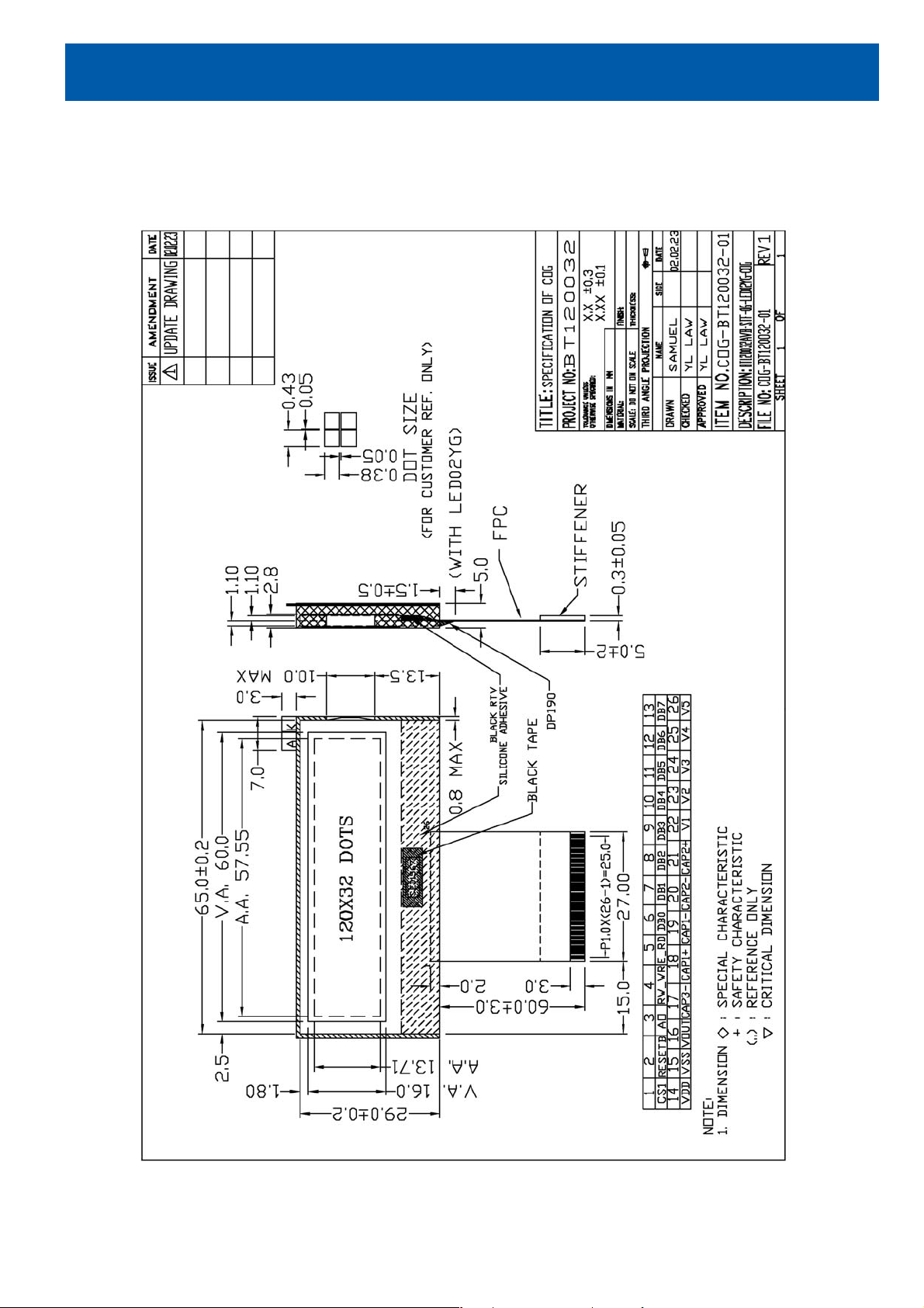
The mechanical detail is shown in Fig. 1 and summarized in Table 1 below.
Table 1
Parameter Specifications Unit
Outline dimensions 66.6(W) x 92.8(H) x 5.0(D) (Module)
65.8(W) x 29.0(H) x 2.8(D) (LCD)
Effective viewing area 60.0(W) x 16.0(H) mm
Active area 57.55(W) x 13.71(H) mm
Display format 120 (W) x 32(H) dots
Dot size 0.43(W) x 0.38(H) mm
Dot spacing 0.05(W) x 0.05(H) mm
Dot pitch 0.48(W) x 0.43(H) mm
Weight: TBD grams
mm
Page 5
BA TRON
BT 120032AVB-STF-12-LED02.YG
5/13
Figure 1: Specification of the COG-BT120032-01 module.
Page 6
BA TRON
BT 120032AVB-STF-12-LED02.YG
V5
V4
V3
6/13
COG-BT120032AVB
16
120 X 32 DOTS
16
120
V2
V1
CAP2+
CAP2-
CAP1-
CAP1+
CAP3-
VOUT
VSS
VDD
DB0~
DB7
E_RD
RW_WR
A0
RESETB
CS1
DOT MATRIX LCD
DRIVER 'EPSON'
SED1567D0B
(COG)
8
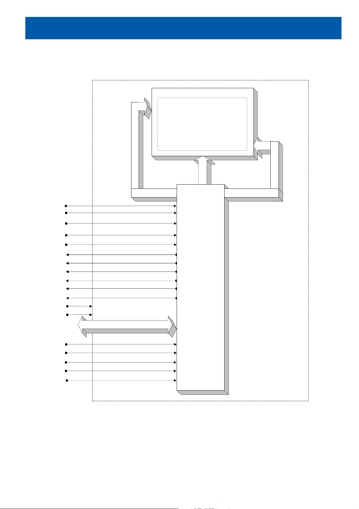
Figure 2: Block Diagram
Page 7
BA TRON
BT 120032AVB-STF-12-LED02.YG
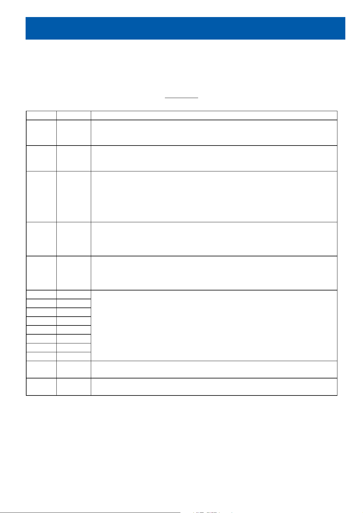
3. Interface signals
Table 2(a)
Pin No. Symbol Description
1 CS1 This is the chip select signal. When CS1 = “L”, then the chip select become
active, and data/command I/O is enabled.
2 RESETB When RESETB is set to “L,” the settings are initialized. The reset operation is
performed by the RESETB signal level.
3 A0 This is connected to the least significant bit of the normal MPU address bus, and
it determines whether the data bits are data or a command.
A0 = “H”: Indicates that DB0 to DB7 are display data.
A0 = “L”: Indicates that DB0 to DB7 are control data.
7/13
4 RW_WR • When connected to an 8080 MPU, this is active LOW. This terminal connects
to the 8080 MPU WR signal. The signals on the data bus are latched at the rising
edge of the WR signal.
5 E_RD • When connected to an 8080 MPU, this is active LOW. This pin is connected to
the RD signal of the 8080 MPU, and the SED1565 series data bus is in an output
status when this signal is “L”.
6 DB0
7 DB1
8 DB2
9 DB3
10 DB4
11 DB5
12 DB6
13 DB7
14 VDD Power supply for logic (+3V).
15 VSS Ground (0V)
This is an 8-bit bi-directional data bus that connects to an 8-bit or 16-bit 8
standard MPU data bus.
Page 8
BA TRON
BT 120032AVB-STF-12-LED02.YG
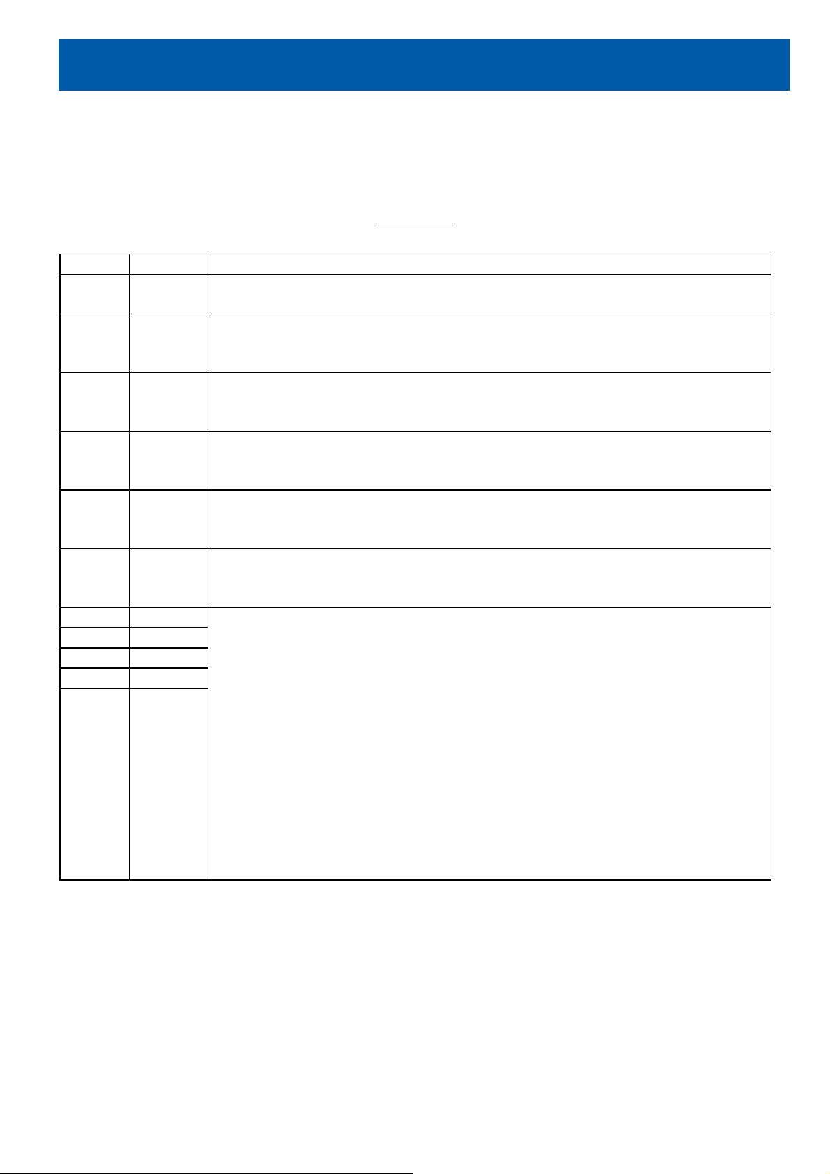
Table 2(b)
Pin No. Symbol Description
16 VOUT DC/DC voltage converter. Connect a capacitor between this terminal and VSS
17 CAP3- DC/DC voltage converter. Connect a capacitor between this terminal and the
CAP1+ terminal.
18 CAP1+ DC/DC voltage converter. Connect a capacitor between this terminal and the
CAP1- terminal.
19 CAP1- DC/DC voltage converter. Connect a capacitor between this terminal and the
CAP1+ terminal.
8/13
20 CAP2- DC/DC voltage converter. Connect a capacitor between this terminal and the
CAP2+ terminal.
21 CAP2+ DC/DC voltage converter. Connect a capacitor between this terminal and the
CAP2- terminal.
22 V1
23 V2
24 V3
25 V4
26 V5
This is a multi-level power supply for the liquid crystal drive. The voltage
applied is determined by the liquid crystal cell, and is changed through the use of
a resistive voltage divided or through changing the impedance using an op. amp.
Voltage levels are determined based on VDD, and must maintain the relative
magnitudes shown below.
VDD (= V0)ЊV1 ЊV2 ЊV3 ЊV4 ЊV5
Master operation: When the power supply turns ON, the internal power supply
circuits produce the V1 to V4 voltages shown below. The voltage settings are
selected using the LCD bias set command.
For 1/6 bias: V1=(1/6)xV5, V2=(2/6)xV5, V3=(4/6)xV5, V4=(5/6)xV5.
Page 9
A
H
V
H
BA TRON
BT 120032AVB-STF-12-LED02.YG
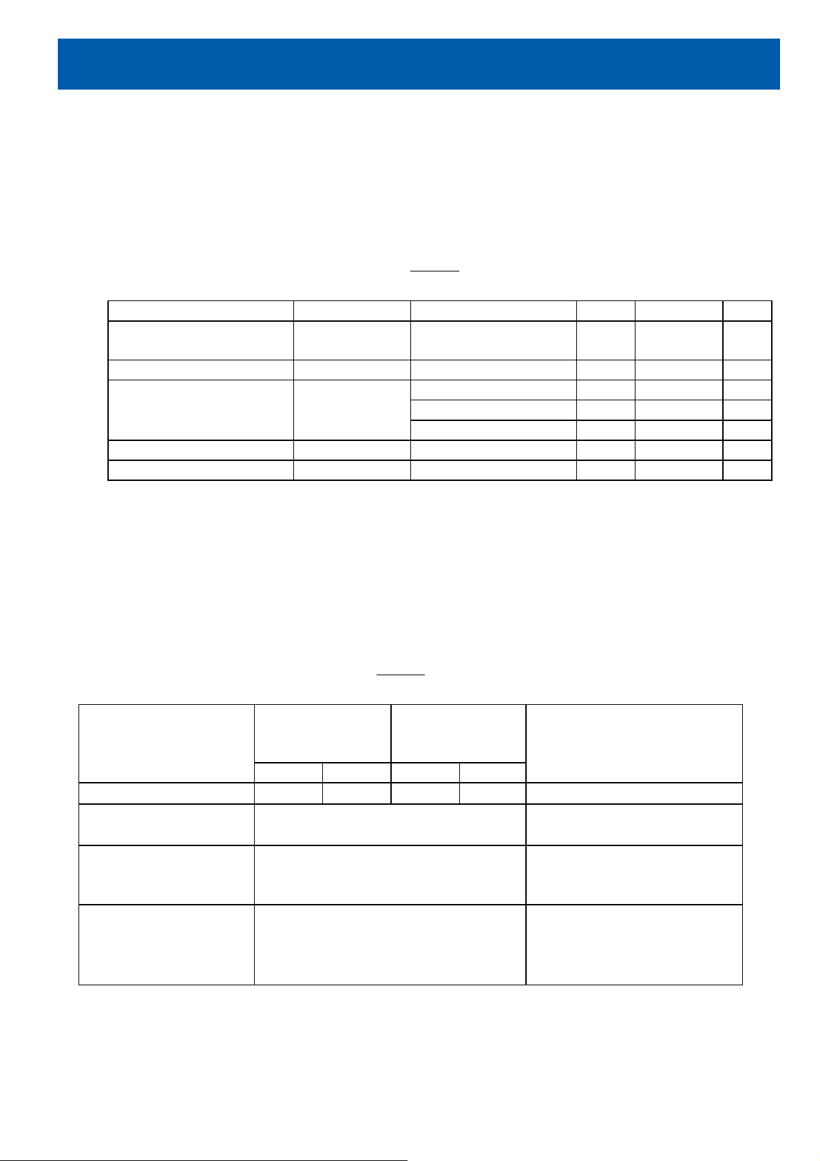
4. Absolute Maximum Ratings
4.1 Electrical Maximum Ratings(Ta = 25 ºC)
Parameter Symbol Conditions Min. Max. Unit
Power Supply voltage
(Logic)
Input voltage Vin -0.3 VDD+0.3 V
Power Supply voltage(2) VSS2
Power Supply voltage(3) V5,VOUT -18.0 +0.3 V
Power Supply voltage(4) V1,V2,V3,V4 V5 +0.3 V
VDD – VSS -0.3 +7.0 V
9/13
Table 3
-7.0 +0.3 V
With Triple step-up -6.0 +0.3 V
With Quad step-up -4.5 +0.3 V
Note:
1.)The modules may be destroyed if they are used beyond the absolute maximum ratings.
2.)All voltage values are referenced to VSS= 0V.
3.) Insure that the voltage levels of V1, V2, V3,and V4 are always such that
VDD ЊV1 ЊV2 ЊV3 ЊV4 ЊV5.
4.2 Environmental Condition
Operating
Item
mbient Temperature
umidity
ibration (IEC 68-2-6)
cells must be mounted
on a suitable connector
Shock (IEC 68-2-27)
alf-sine pulse shape
Temperature
(Topr)
Min. Max. Min. Max.
0°C +50°C -20°C +60°C
95% max. RH for Ta ≤ 40°C
< 95% RH for Ta > 40°C
Frequency: 10 ∼ 55 Hz
Amplitude: 0.75 mm
Duration: 20 cycles in each direction.
Pulse duration : 11 ms
Peak acceleration: 981 m/s2= 100g
Number of shocks : 3 shocks in 3
mutually perpendicular axes.
Table 4
Storage
Temperature
(Tstg)
Remark
Dry
no condensation
3 directions
3 directions
Page 10
BA TRON
BT 120032AVB-STF-12-LED02.YG
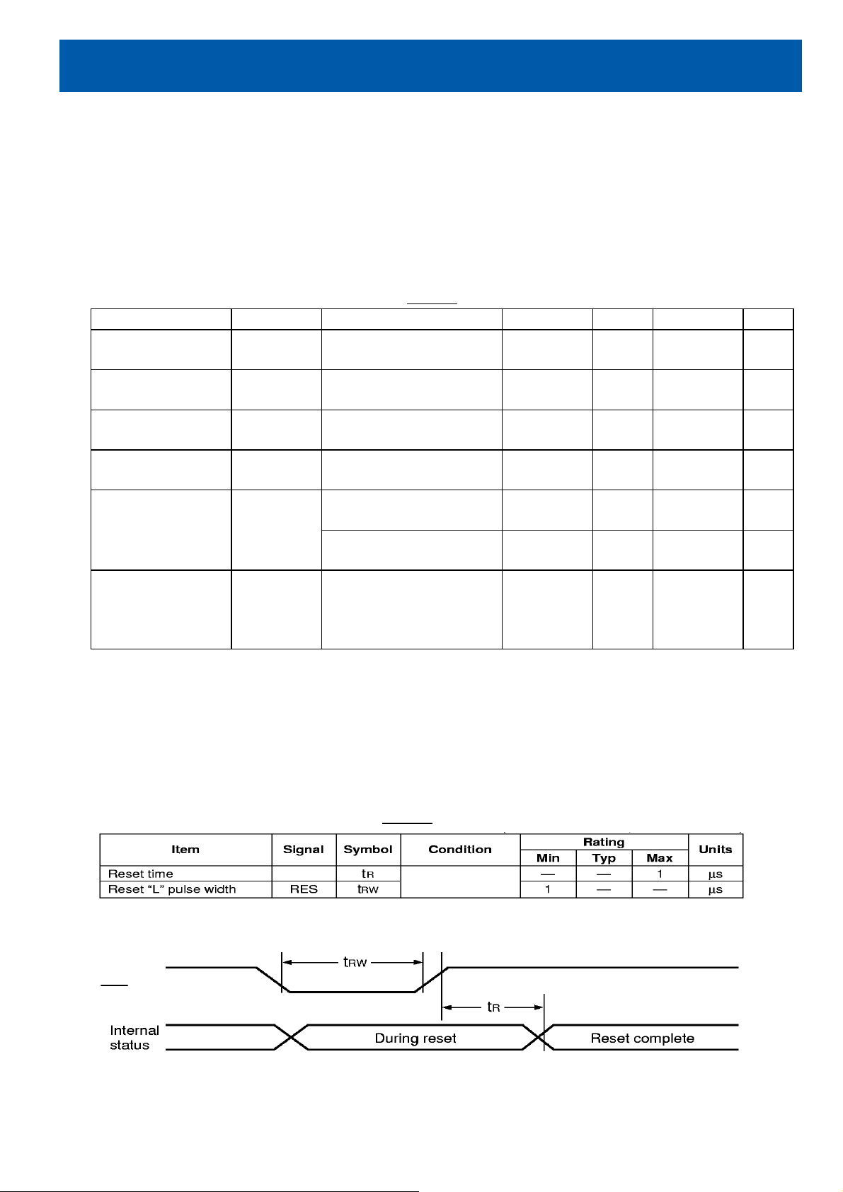
5. Electrical Specifications
5.1 Typical Electrical Characteristics
At Ta = 25 °C, VDD = 3V±0.2V, VSS=0V.
Parameter Symbol Conditions Min. Typ. Max. Unit
Supply voltage
VDD-VSS 2.8 3.0 3.2 V
(Logic)
Supply voltage
(LCD)
Low-level input
VLCD
=VDD-V5
V
VSS - 0.2xVDD V
ILC
VDD = +3.0V,
Note 1
signal voltage
High-level input
V
0.8xVDD - VDD V
IHC
signal voltage
IDD
(Logic & LCD)
Character mode,
VDD = +3.0V
Checker board
mode,VDD = +3.0V
Supply voltage of
yellow-green
LED02 backlight
Number of LED
chips=2x5=10.
Forward current
=75mA.
10/13
Table 5
6.2 6.5 6.8 V
- 163 213.5 µA Supply Current
- 261 302 µA
4.0 4.1 4.2 V
Note (1) : There is tolerance in optimum LCD driving voltage during production and it will be within
the specified range.
5.2 Timing Specifications
Reset Timing
At Ta = 0 °°°°C to +50 °°°°C, VDD = +3V±±±±0.2V, VSS = 0V.
Table 6
Note :All timing is specified with 20% and 80% of VDD as the standard.
RESETB
(RES)
Figure 3:Reset Timing
Page 11
(
)
(
)
BA TRON
BT 120032AVB-STF-12-LED02.YG
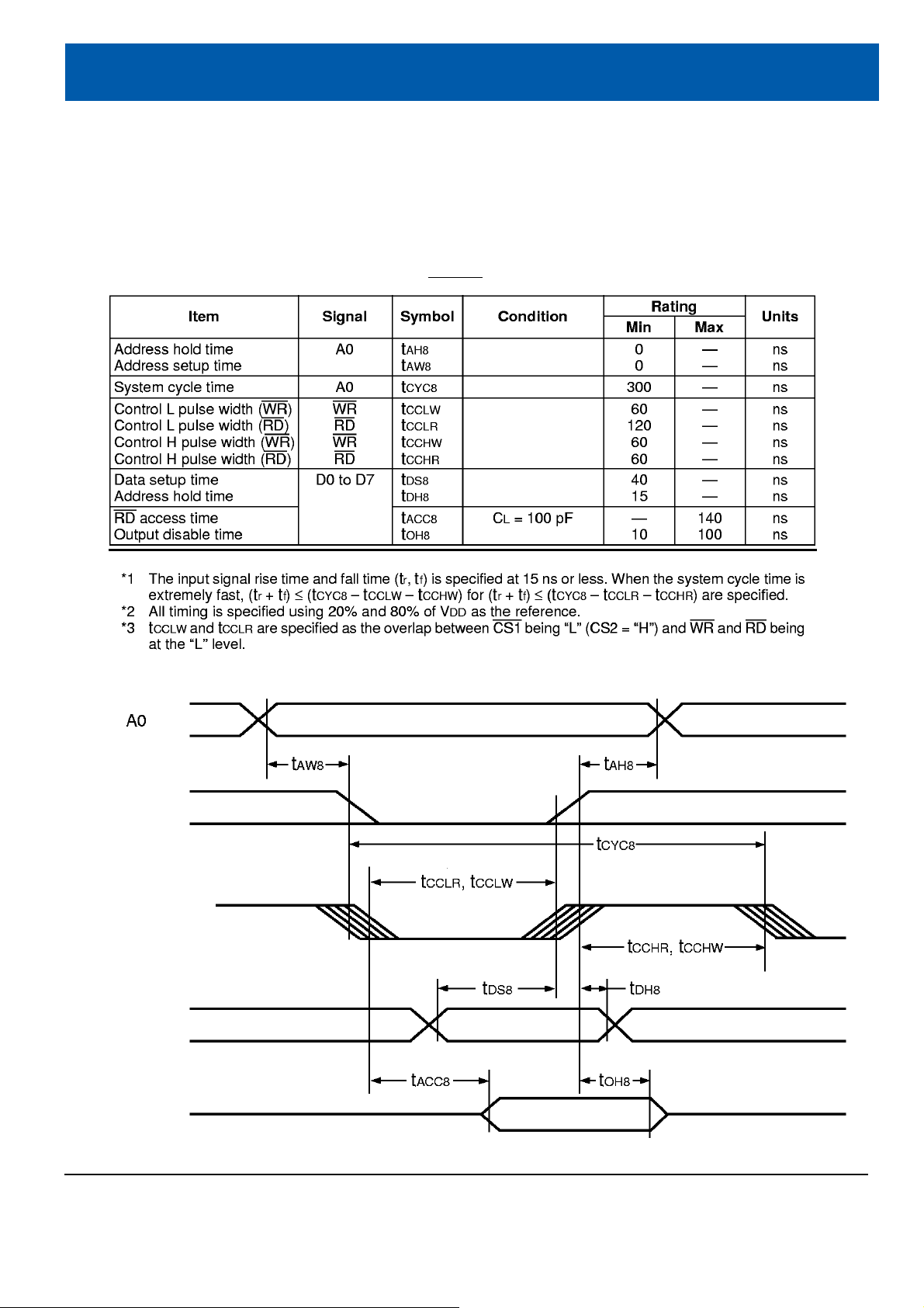
System Bus Read/Write Characteristics (For the 8080 Series MPU)
At Ta = 0 °°°°C to +50 °°°°C, VDD = +3V±±±±0.2V, VSS = 0V.
Table 7
11/13
CS1
RW_WR,E_RD
(WR,RD)
DB0 to DB7
(D0 to D7)
Write
DB0 to DB7
(D0 to D7)
Read
Figure 4: MPU bus read / write timing diagram (80 family MPU)
Page 12
BA TRON
BT 120032AVB-STF-12-LED02.YG
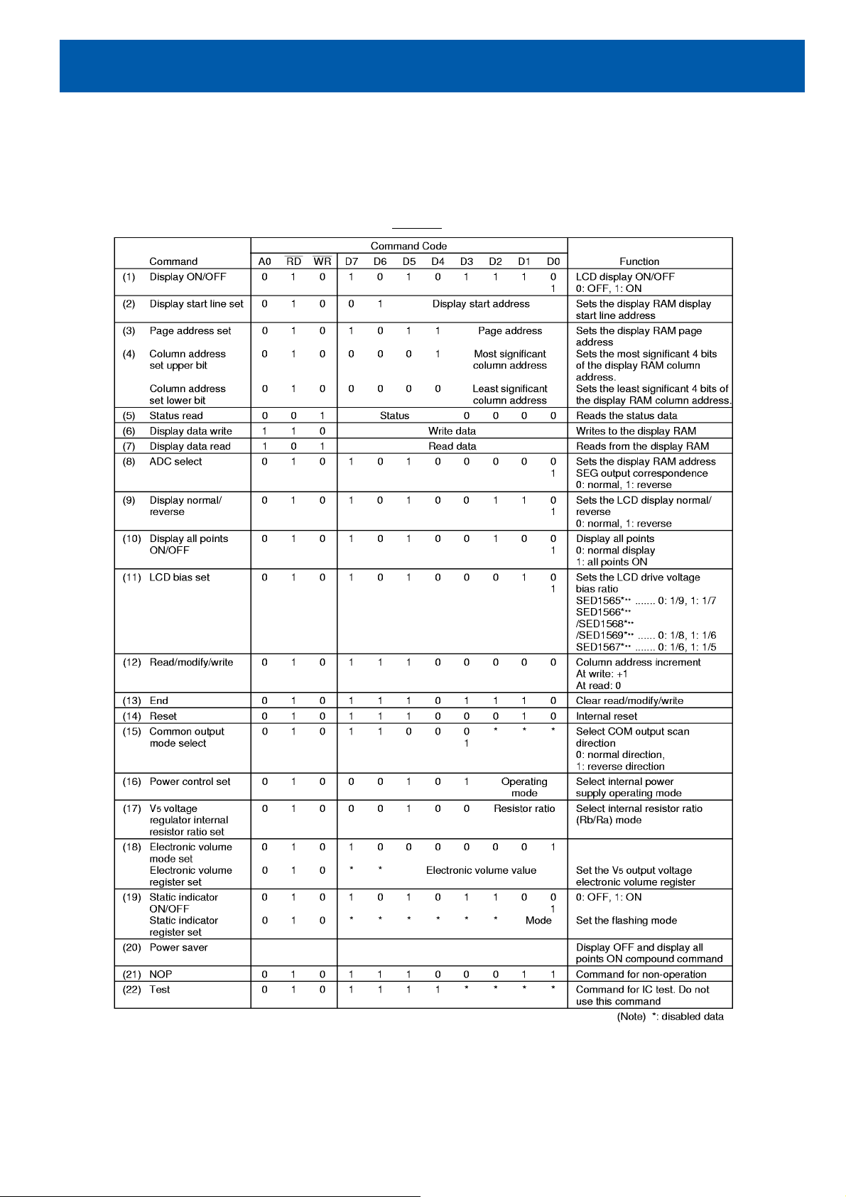
5.3 Instruction Set
12/13
Table 8
Page 13
BA TRON
BT 120032AVB-STF-12-LED02.YG
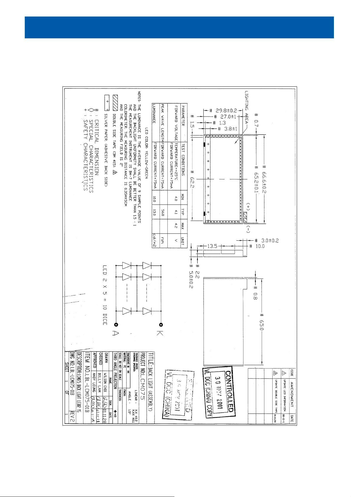
6. LED Backlight Specification
13/13
 Loading...