

Page 1
CN8330
DS3/E3 Framer with 52 Mbps HDLC Controller
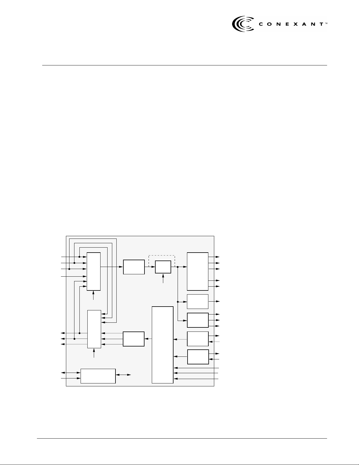
The CN8330 is an integral DS3/E3 framer designed to support the transmission
formats defined by ANSI T1.107-1988, T1.107a-1989, T1.404, and ITU-T G.751
standards. All maintenance features required by Bellcore TR-TSY-000009 and AT&T
PUB 54014 are provided. In addition, the CN8330 can be optionally configured as a
High-Level Data Link Controller (HDLC) usable with or without DS3/E3 framing
overhead.
The CN8330 provides framing recovery for M13, C-bit parity, Syntran, and G.751
E3 formatted signals. A First In First Out (FIFO) buffer in the receive path can be
enabled to reduce jitter on the incomi ng data. Transmi t and recei ve data is availabl e to
the host in either serial or parallel byte and nibble formats. Access is provided to the
terminal data link and the Far End Alarm/Control (FEAC) channel, as specified in
T1.107a-1989. Counters are included for frame-bit errors, Line Code Violations
(LCVs), parity errors, and Far End Block Errors (FEBEs).
Two operational modes are available: microprocessor and stand-alone monitor
control modes. The microprocessor control mode monitors all status conditions and
provides configuration control. The stand-alone monitor mode allows the CN8330 to
operate as a monitor providing status and alarm information on external pins.
Functional Block Diagram
RXPOS
RXNEG
DS3CKI
TXCKI
TXPOS
TXNEG
TCLKO
AD[7:0]
Control
M
U
X
Source
Loopback
M
U
X
Line
Loopback
Microprocessor
Interface
Unipolar
Conversion
Bipolar
Encoder
To/From
All Blocks
Bypass
FIFO
FIFO
Enable
Framing/
Overhead
Insertion
Framing
Recovery
Overhead/
Data Link
Processing
PPDL
Receiver
PPDL
Transmitter
Overhead/
Data Link
Processing
RXMSY
CBITO
RXCCK
RXDAT
RXCLK
Status
RDAT[7:0]
RXBCK
Status
TXBCK
TDAT[7:0]
TXCCK
CBITI
TXCKI
TXDATI
TXSYI
Distinguishing Features
• Supports DS3/E3 framing modes
• Includes high-speed HDLC controller
(52 MHz)
• Framing recovery for M13, C-bit
parity, Syntran, and G.751 E3 signals
• Serial or parallel (octet or nibble)
interface modes
• Average reframe time of less than
1 ms for DS3 and less than 250 µs
for E3
• Supports the LAP D term inal da ta li nk
and FEAC channel as defined in
T1.107a-1989
• 68-pin PLCC or 80-pin MQFP
surface-mount package
• Operates from a single +5 VDC ±5%
power supply
• Low-power CM OS tec h no lo gy
Applications
• Digital PCM switche s
• Digital Cross-Connect Systems
• Channel Service Units (CSUs )
• Channel extenders
• ATM Switches/Concentrators
•PBXs
• Switched Multimegabit Digital
Service (SMDS) Equipment
• Test equi pm e n t
• Routers (in c luding HSSI por ts)
Data Sheet 100441E
October 13, 1999
Page 2
Ordering Information
Model Number Package Ambient Temperature
CN8330EPJD 68-Pin Plastic Leaded Chip Carrier (PLCC)
CN8330EPD 80-Pin Metric Quad Flat Pack (MQFP)
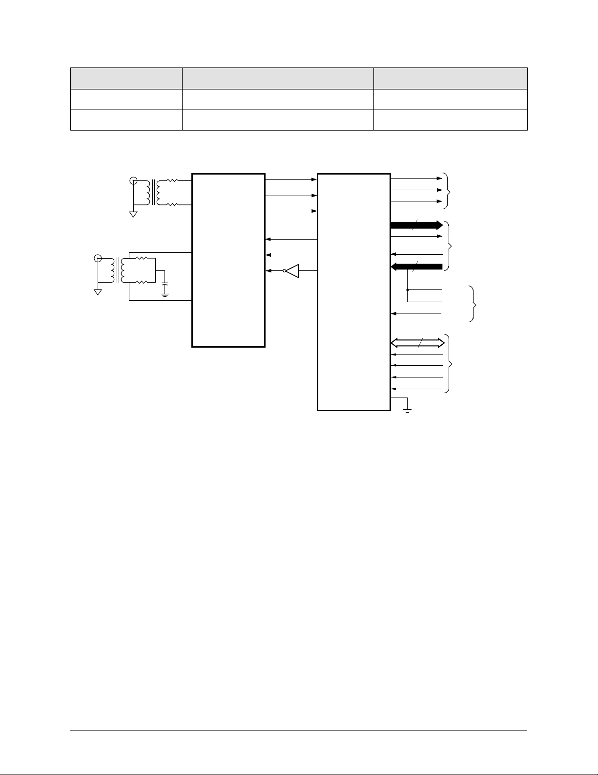
CN8330 Typical DS3 Application
31.6Ω
31.6Ω
37.4Ω
37.4Ω
0.01
RLINE1P
RLINE1N
TLINE1P
TLINE1N
CN8331
RPOS1
RNEG1
RCLK1
TPOS1
TNEG1
TCLK1
CN8330
DS3/E3 Framer
RXPOS
RXNEG
DS3CKI
TXPOS
TXNEG
TCLKO
RXDAT
RXCLK
RXMSY
RDAT[7:0]
RXBCK
TXBCK
TDAT[7:0]
TXCKI
AD[7:0]
RD*
WR*
CS
ALE
MON/MIC*
8
8
TDAT7
TDAT6
8
–40 to 85
–40 to 85
Receive
Serial
Data
Interface
Parallel
Data
Interface
(Also used
for HDLC
payload
data)
(M-Sync)
(Data)
(Clock)
° C
° C
Transmit
Serial
Data
Interface
Microprocessor
Interface
Information provided by Conexant Systems, Inc. (Conexant) is believed to be accurate and reliable. However, no responsibility is
assumed by Conexant for its use, nor any infringement of patents or other rights of third parties which may result from its use. No
license is granted by implication or otherwise under any patent rights of Conexant other than for circuitry embodied in Conexant
products. Conexant reserves the right to change circuitry at any time without notice. This document is subject to change without
notice.
Conexant products are not designed or intended for use in life support appliances, devices, or systems where malfunction of a
Conexant product can reasonably be expected to result in personal injury or death. Conexant customers using or selling Conexant
products for use in such applications do so at their own risk and agree to fully indemnify Conexant for any damages resulting from
such improper use or sale.
The trademarks “Conexant” and the Conexant symbol are trademarks of Conexant Systems, Inc.
Product names or services listed in this publication are for identification purposes only, and may be trademarks or registered
trademarks of their respective companies. All other marks mentioned herein are the property of their respective holders.
© 1999 Conexant Systems, Inc.
Printed in U.S.A.
All Rights Reserved
Reader Response: Conexant strives to produce quality documentation, and welcomes your feedback. Please send
comments and suggestions to [email protected]. For technical questions, contact your local
Conexant sales office or field applications engineer.
100441E Conexant
Page 3

Table of Contents
List of Figures . . . . . . . . . . . . . . . . . . . . . . . . . . . . . . . . . . . . . . . . . . . . . . . . . . . . . . . . . . . . . . . . . . . . . . . . . v
List of Tables . . . . . . . . . . . . . . . . . . . . . . . . . . . . . . . . . . . . . . . . . . . . . . . . . . . . . . . . . . . . . . . . . . . . . . . . . vii
1.0 Product Description. . . . . . . . . . . . . . . . . . . . . . . . . . . . . . . . . . . . . . . . . . . . . . . . . . . . . . . . . . . . . 1-1
1.1 Pin Descriptions . . . . . . . . . . . . . . . . . . . . . . . . . . . . . . . . . . . . . . . . . . . . . . . . . . . . . . . . . . . . 1-3
2.0 Functional Description. . . . . . . . . . . . . . . . . . . . . . . . . . . . . . . . . . . . . . . . . . . . . . . . . . . . . . . . . . 2-1
2.1 Overview. . . . . . . . . . . . . . . . . . . . . . . . . . . . . . . . . . . . . . . . . . . . . . . . . . . . . . . . . . . . . . . . . . 2-1
2.1.1 Brief Block Description. . . . . . . . . . . . . . . . . . . . . . . . . . . . . . . . . . . . . . . . . . . . . . . . . . 2-1
2.1.2 Clock Interface and Initialization . . . . . . . . . . . . . . . . . . . . . . . . . . . . . . . . . . . . . . . . . . . 2-3
2.1.2.1 Initialization . . . . . . . . . . . . . . . . . . . . . . . . . . . . . . . . . . . . . . . . . . . . . . . . . 2-3
2.1.3 Microprocessor Interface . . . . . . . . . . . . . . . . . . . . . . . . . . . . . . . . . . . . . . . . . . . . . . . . 2-3
2.1.3.1 Using with Specific Microcontrollers . . . . . . . . . . . . . . . . . . . . . . . . . . . . . . . 2-3
2.1.3.2 Microprocessor Interrupts. . . . . . . . . . . . . . . . . . . . . . . . . . . . . . . . . . . . . . . 2-4
2.1.3.3 Address Map . . . . . . . . . . . . . . . . . . . . . . . . . . . . . . . . . . . . . . . . . . . . . . . . 2-4
2.2 Line Interfaces . . . . . . . . . . . . . . . . . . . . . . . . . . . . . . . . . . . . . . . . . . . . . . . . . . . . . . . . . . . . . 2-5
2.2.1 Transmitter Line Interface. . . . . . . . . . . . . . . . . . . . . . . . . . . . . . . . . . . . . . . . . . . . . . . . 2-5
2.2.2 Receiver Line Interface. . . . . . . . . . . . . . . . . . . . . . . . . . . . . . . . . . . . . . . . . . . . . . . . . . 2-6
2.3 Transmitter Operation . . . . . . . . . . . . . . . . . . . . . . . . . . . . . . . . . . . . . . . . . . . . . . . . . . . . . . . . 2-7
2.3.1 Input and Synchronization . . . . . . . . . . . . . . . . . . . . . . . . . . . . . . . . . . . . . . . . . . . . . . . 2-7
2.3.2 DS3 Mode . . . . . . . . . . . . . . . . . . . . . . . . . . . . . . . . . . . . . . . . . . . . . . . . . . . . . . . . . . . 2-7
2.3.3 E3 Mode . . . . . . . . . . . . . . . . . . . . . . . . . . . . . . . . . . . . . . . . . . . . . . . . . . . . . . . . . . . . 2-9
2.3.4 Fra ming Bit Gener ation. . . . . . . . . . . . . . . . . . . . . . . . . . . . . . . . . . . . . . . . . . . . . . . . . 2-10
2.3.5 Alarm Signal Generation. . . . . . . . . . . . . . . . . . . . . . . . . . . . . . . . . . . . . . . . . . . . . . . . 2-11
2.3.6 Terminal Data Link Transmitter . . . . . . . . . . . . . . . . . . . . . . . . . . . . . . . . . . . . . . . . . . . 2-12
2.3.6.1 Sending a Message. . . . . . . . . . . . . . . . . . . . . . . . . . . . . . . . . . . . . . . . . . . 2-13
2.3.6.2 Aborting a Message . . . . . . . . . . . . . . . . . . . . . . . . . . . . . . . . . . . . . . . . . . 2-14
2.3.6.3 Transmitter Interrupts . . . . . . . . . . . . . . . . . . . . . . . . . . . . . . . . . . . . . . . . . 2-14
2.3.6.4 Transmitter Control Example . . . . . . . . . . . . . . . . . . . . . . . . . . . . . . . . . . . . 2-15
2.3.7 TxFEAC Channel Transmission . . . . . . . . . . . . . . . . . . . . . . . . . . . . . . . . . . . . . . . . . . . 2-15
2.3.8 PPDL Transmitter. . . . . . . . . . . . . . . . . . . . . . . . . . . . . . . . . . . . . . . . . . . . . . . . . . . . . 2-16
2.3.9 PPDLONLY Mode. . . . . . . . . . . . . . . . . . . . . . . . . . . . . . . . . . . . . . . . . . . . . . . . . . . . . 2-20
2.3.10 Transmitter Outputs . . . . . . . . . . . . . . . . . . . . . . . . . . . . . . . . . . . . . . . . . . . . . . . . . . . 2-20
2.3.11 Test Equipment Specific Features . . . . . . . . . . . . . . . . . . . . . . . . . . . . . . . . . . . . . . . . . 2-21
100441E Conexant i
Page 4

CN8330
DS3/E3 Framer with 52 Mbps HDLC Controller
2.4 Receiver Operation. . . . . . . . . . . . . . . . . . . . . . . . . . . . . . . . . . . . . . . . . . . . . . . . . . . . . . . . . 2-22
2.4.1 Bipolar-to-Unipolar Conversion. . . . . . . . . . . . . . . . . . . . . . . . . . . . . . . . . . . . . . . . . . . 2-22
2.4.2 Receive FIFO . . . . . . . . . . . . . . . . . . . . . . . . . . . . . . . . . . . . . . . . . . . . . . . . . . . . . . . . 2-22
2.4.3 Received Signal Output . . . . . . . . . . . . . . . . . . . . . . . . . . . . . . . . . . . . . . . . . . . . . . . . 2-23
2.4.4 Fr aming Operat ion . . . . . . . . . . . . . . . . . . . . . . . . . . . . . . . . . . . . . . . . . . . . . . . . . . . . 2-25
2.4.5 Alarm Detection. . . . . . . . . . . . . . . . . . . . . . . . . . . . . . . . . . . . . . . . . . . . . . . . . . . . . . 2-25
2.4.6 Terminal Data Link Reception . . . . . . . . . . . . . . . . . . . . . . . . . . . . . . . . . . . . . . . . . . . . 2-26
2.4.6.1 Receiver Interrupts . . . . . . . . . . . . . . . . . . . . . . . . . . . . . . . . . . . . . . . . . . . 2-28
2.4.6.2 Receiver Response Example . . . . . . . . . . . . . . . . . . . . . . . . . . . . . . . . . . . . 2-28
2.4.7 RxFEAC Channel Reception. . . . . . . . . . . . . . . . . . . . . . . . . . . . . . . . . . . . . . . . . . . . . . 2-29
2.4.8 PPDL Receiver. . . . . . . . . . . . . . . . . . . . . . . . . . . . . . . . . . . . . . . . . . . . . . . . . . . . . . . 2-30
2.4.9 PPDLONLY Mode. . . . . . . . . . . . . . . . . . . . . . . . . . . . . . . . . . . . . . . . . . . . . . . . . . . . . 2-32
2.4.10 Serial C-Bit Output . . . . . . . . . . . . . . . . . . . . . . . . . . . . . . . . . . . . . . . . . . . . . . . . . . . . 2-33
2.5 Monito r Mode for Stand-Alone Operation . . . . . . . . . . . . . . . . . . . . . . . . . . . . . . . . . . . . . . . . 2-34
2.5.1 DS3 Monitor Mode Error Outputs. . . . . . . . . . . . . . . . . . . . . . . . . . . . . . . . . . . . . . . . . 2-35
3.0 Registers . . . . . . . . . . . . . . . . . . . . . . . . . . . . . . . . . . . . . . . . . . . . . . . . . . . . . . . . . . . . . . . . . . . . . . 3-1
3.1 Control Registers . . . . . . . . . . . . . . . . . . . . . . . . . . . . . . . . . . . . . . . . . . . . . . . . . . . . . . . . . . . 3-1
0x00—Mode Control Register (CR00). . . . . . . . . . . . . . . . . . . . . . . . . . . . . . . . . . . . . . . 3-1
0x01—Terminal Data Link Control Register (CR01) . . . . . . . . . . . . . . . . . . . . . . . . . . . . . 3-3
0x02—Status Interrupt Control Register (CR02) . . . . . . . . . . . . . . . . . . . . . . . . . . . . . . . 3-3
0x03—Transmit FEAC Channel Byte (CR03) . . . . . . . . . . . . . . . . . . . . . . . . . . . . . . . . . . 3-4
0x04—Feature Control Register (CR04) . . . . . . . . . . . . . . . . . . . . . . . . . . . . . . . . . . . . . 3-4
0x05—PPDL Control Register (CR05). . . . . . . . . . . . . . . . . . . . . . . . . . . . . . . . . . . . . . . 3-5
3.2 Status Registers. . . . . . . . . . . . . . . . . . . . . . . . . . . . . . . . . . . . . . . . . . . . . . . . . . . . . . . . . . . . 3-6
0x10—DS3/E3 Maintenance Status Register (SR00). . . . . . . . . . . . . . . . . . . . . . . . . . . . 3-6
0x11—Counter Interrupt Status Register (SR01). . . . . . . . . . . . . . . . . . . . . . . . . . . . . . . 3-7
0x12—Data Link Interrupt Status Register (SR02) . . . . . . . . . . . . . . . . . . . . . . . . . . . . . 3-8
0x13—Receive FEAC Channel Byte (SR03) . . . . . . . . . . . . . . . . . . . . . . . . . . . . . . . . . . . 3-8
0x14—Terminal Data Link Status Register (SR04). . . . . . . . . . . . . . . . . . . . . . . . . . . . . . 3-9
0x15—Part Number/Hardware Version Register (SR05) . . . . . . . . . . . . . . . . . . . . . . . . . 3-9
0x16—Shadow Status Register (SR06) . . . . . . . . . . . . . . . . . . . . . . . . . . . . . . . . . . . . 3-10
0x20–0x26—DS3/E3 Error Counters. . . . . . . . . . . . . . . . . . . . . . . . . . . . . . . . . . . . . . . 3-11
0x20—DS3 Parity Error Counter (SR07). . . . . . . . . . . . . . . . . . . . . . . . . . . . . . . . . . . . 3-11
0x21—DS3 Disagreement Counter (SR08) . . . . . . . . . . . . . . . . . . . . . . . . . . . . . . . . . . 3-12
0x22—DS3/E3 Frame Error Counter (SR09) . . . . . . . . . . . . . . . . . . . . . . . . . . . . . . . . . 3-12
0x23—DS3 Path Parity Error Counter (SR10). . . . . . . . . . . . . . . . . . . . . . . . . . . . . . . . 3-12
0x24—DS3 FEBE Event Counter (SR11) . . . . . . . . . . . . . . . . . . . . . . . . . . . . . . . . . . . . 3-13
0x25,0x26—DS3/E3 LCV Counter—Low and High Bytes (SR12,SR13) . . . . . . . . . . . . . 3-13
3.3 Memory Registers . . . . . . . . . . . . . . . . . . . . . . . . . . . . . . . . . . . . . . . . . . . . . . . . . . . . . . . . . 3-14
0x30–0x37—Transmit Terminal Data Link Message Buffer (TxTDL) . . . . . . . . . . . . . . . . 3-14
0x40–0x47—Receive Terminal Data Link Message Buffer (RxTDL) . . . . . . . . . . . . . . . . 3-14
3.4 Register Summary . . . . . . . . . . . . . . . . . . . . . . . . . . . . . . . . . . . . . . . . . . . . . . . . . . . . . . . . . 3-15
ii Conexant 100441E
Page 5

CN8330
DS3/E3 Framer with 52 Mbps HDLC Controller
4.0 Mechanical/Electrical Specifications. . . . . . . . . . . . . . . . . . . . . . . . . . . . . . . . . . . . . . . . . . . . . 4-1
4.1 Timing Requirements . . . . . . . . . . . . . . . . . . . . . . . . . . . . . . . . . . . . . . . . . . . . . . . . . . . . . . . . 4-1
4.2 Environmental Conditions. . . . . . . . . . . . . . . . . . . . . . . . . . . . . . . . . . . . . . . . . . . . . . . . . . . . . 4-5
4.2.1 Power Requirements and Temperature Range . . . . . . . . . . . . . . . . . . . . . . . . . . . . . . . . . 4-5
4.3 Electrical Characteristics . . . . . . . . . . . . . . . . . . . . . . . . . . . . . . . . . . . . . . . . . . . . . . . . . . . . . 4-6
4.3.1 DC Characteristics . . . . . . . . . . . . . . . . . . . . . . . . . . . . . . . . . . . . . . . . . . . . . . . . . . . . . 4-6
4.4 Mechanical Specifications . . . . . . . . . . . . . . . . . . . . . . . . . . . . . . . . . . . . . . . . . . . . . . . . . . . . 4-8
Appendix A Multimegabit HDLC Formatter. . . . . . . . . . . . . . . . . . . . . . . . . . . . . . . . . . . . . . . . . . . . . . A-1
A.1 Introduction . . . . . . . . . . . . . . . . . . . . . . . . . . . . . . . . . . . . . . . . . . . . . . . . . . . . . . . . . . . . . . . A-1
A.2 Block and Logic Diagrams. . . . . . . . . . . . . . . . . . . . . . . . . . . . . . . . . . . . . . . . . . . . . . . . . . . . . A-3
A.3 PPDL Transmitter . . . . . . . . . . . . . . . . . . . . . . . . . . . . . . . . . . . . . . . . . . . . . . . . . . . . . . . . . . . A-6
A.3.1 PPDL Receiver. . . . . . . . . . . . . . . . . . . . . . . . . . . . . . . . . . . . . . . . . . . . . . . . . . . . . . . A-7
Appendix B . . . . . . . . . . . . . . . . . . . . . . . . . . . . . . . . . . . . . . . . . . . . . . . . . . . . . . . . . . . . . . . . . . . . . . . . . . B-1
B.1 DS3CKI Clock Duty Cycle. . . . . . . . . . . . . . . . . . . . . . . . . . . . . . . . . . . . . . . . . . . . . . . . . . . . . . B-1
B.2 Overhead Bit Insertion in E3 Parallel Payload Mode . . . . . . . . . . . . . . . . . . . . . . . . . . . . . . . . . B-1
B.3 HDLC Formatter Mode Support While Config ured for E3 Framing . . . . . . . . . . . . . . . . . . . . . . . B-2
Appendix C . . . . . . . . . . . . . . . . . . . . . . . . . . . . . . . . . . . . . . . . . . . . . . . . . . . . . . . . . . . . . . . . . . . . . . . . . . C-1
100441E Conexant iii
Page 6

CN8330
DS3/E3 Framer with 52 Mbps HDLC Controller
iv Conexant 100441E
Page 7

CN8330 List of Figures
DS3/E3 Framer with 52 Mbps HDLC Controller
List of Figures
Figure 1-1. CN8330 Pinout Diagram - 68-Pin PLCC . . . . . . . . . . . . . . . . . . . . . . . . . . . . . . . . . . . . . . . 1-3
Figure 1-2. CN8330 Pinout Diagram - 80-Pin MQFP. . . . . . . . . . . . . . . . . . . . . . . . . . . . . . . . . . . . . . . 1-4
Figure 1-3. CN8330 Framer Functional Logic Diagram - 68-Pin PLCC . . . . . . . . . . . . . . . . . . . . . . . . . 1-6
Figure 1-4. CN8330 Framer Functional Logic Diagram - 80-Pin MQFP . . . . . . . . . . . . . . . . . . . . . . . . . 1-7
Figure 2-1. Functional Block Diagram . . . . . . . . . . . . . . . . . . . . . . . . . . . . . . . . . . . . . . . . . . . . . . . . . . 2-2
Figure 2-2. Transmitter Line Driver Outputs . . . . . . . . . . . . . . . . . . . . . . . . . . . . . . . . . . . . . . . . . . . . . 2-5
Figure 2-3. Clocked Receiver Input . . . . . . . . . . . . . . . . . . . . . . . . . . . . . . . . . . . . . . . . . . . . . . . . . . . . 2-6
Figure 2-4. Transmitter Timing for Serial DS3 Mode. . . . . . . . . . . . . . . . . . . . . . . . . . . . . . . . . . . . . . . 2-8
Figure 2-5. Transmitter Timing for Parallel DS3 Mode . . . . . . . . . . . . . . . . . . . . . . . . . . . . . . . . . . . . . 2-9
Figure 2-6. Transmitter Timing for Serial E3 Mode . . . . . . . . . . . . . . . . . . . . . . . . . . . . . . . . . . . . . . . 2-10
Figure 2-7. C-Bit Input Timing. . . . . . . . . . . . . . . . . . . . . . . . . . . . . . . . . . . . . . . . . . . . . . . . . . . . . . . 2-11
Figure 2-8. PPDL Transmitter Timing . . . . . . . . . . . . . . . . . . . . . . . . . . . . . . . . . . . . . . . . . . . . . . . . . 2-17
Figure 2-9. Nibble Mode with the PPDLONLY Control Pin Low. . . . . . . . . . . . . . . . . . . . . . . . . . . . . . 2-19
Figure 2-10. VCO Output Signal Timing. . . . . . . . . . . . . . . . . . . . . . . . . . . . . . . . . . . . . . . . . . . . . . . . . 2-22
Figure 2-11. Receiver Timing for Serial DS3 Mode . . . . . . . . . . . . . . . . . . . . . . . . . . . . . . . . . . . . . . . . 2-23
Figure 2-12. Receiver Timing for Parallel DS3 Mode. . . . . . . . . . . . . . . . . . . . . . . . . . . . . . . . . . . . . . . 2-24
Figure 2-13. E3 Receiver Output Timing . . . . . . . . . . . . . . . . . . . . . . . . . . . . . . . . . . . . . . . . . . . . . . . . 2-24
Figure 2-14. PPDL Receiver Timing. . . . . . . . . . . . . . . . . . . . . . . . . . . . . . . . . . . . . . . . . . . . . . . . . . . . 2-31
Figure 2-15. C-Bit Output Timing. . . . . . . . . . . . . . . . . . . . . . . . . . . . . . . . . . . . . . . . . . . . . . . . . . . . . . 2-33
Figure 2-16. Monitor Mode Error Indication Timing . . . . . . . . . . . . . . . . . . . . . . . . . . . . . . . . . . . . . . . 2-35
Figure 4-1. Microprocessor Interface Timing . . . . . . . . . . . . . . . . . . . . . . . . . . . . . . . . . . . . . . . . . . . . 4-2
Figure 4-2. Output and Input Signal Timing. . . . . . . . . . . . . . . . . . . . . . . . . . . . . . . . . . . . . . . . . . . . . . 4-3
Figure 4-3. 68–Pin Plastic Leaded Chip Carrier (J-Bend) . . . . . . . . . . . . . . . . . . . . . . . . . . . . . . . . . . . 4-8
Figure 4-4. 80-Pin Metric Quad Flat Pack (MQFP). . . . . . . . . . . . . . . . . . . . . . . . . . . . . . . . . . . . . . . . . 4-9
Figure A-1. HDLC Formatter Block Diagram . . . . . . . . . . . . . . . . . . . . . . . . . . . . . . . . . . . . . . . . . . . . .A-2
Figure A-2. HDLC Formatter Logic Diagram . . . . . . . . . . . . . . . . . . . . . . . . . . . . . . . . . . . . . . . . . . . . .A-4
Figure A-3. HDLC Formatter Logic Diagram - 80-Pin MQFP . . . . . . . . . . . . . . . . . . . . . . . . . . . . . . . . . A-5
Figure A-4. PPDL Transmitter Timing . . . . . . . . . . . . . . . . . . . . . . . . . . . . . . . . . . . . . . . . . . . . . . . . . . A-6
Figure A-5. PPDL Receiver Timing. . . . . . . . . . . . . . . . . . . . . . . . . . . . . . . . . . . . . . . . . . . . . . . . . . . . . A-9
100441E Conexant v
Page 8

List of Figures CN8330
DS3/E3 Framer with 52 Mbps HDLC Controller
vi Conexant 100441E
Page 9

CN8330 List of Tables
DS3/E3 Framer with 52 Mbps HDLC Controller
List of Tables
Table 1-1. Pin Descriptions . . . . . . . . . . . . . . . . . . . . . . . . . . . . . . . . . . . . . . . . . . . . . . . . . . . . . . . . . . 1-5
Table 1-2. Hardware Signal Definitions . . . . . . . . . . . . . . . . . . . . . . . . . . . . . . . . . . . . . . . . . . . . . . . . . 1-8
Table 2-1. Transmit Encoding Options. . . . . . . . . . . . . . . . . . . . . . . . . . . . . . . . . . . . . . . . . . . . . . . . . 2-20
Table 3-1. Register Overview. . . . . . . . . . . . . . . . . . . . . . . . . . . . . . . . . . . . . . . . . . . . . . . . . . . . . . . . 3 -15
Table 3-2. Status Registers . . . . . . . . . . . . . . . . . . . . . . . . . . . . . . . . . . . . . . . . . . . . . . . . . . . . . . . . . 3-15
Table 3-3. Transmit Terminal Data Link Message Buffer . . . . . . . . . . . . . . . . . . . . . . . . . . . . . . . . . . . 3-16
Table 3-4. Receive Terminal Data Link Message Buffer . . . . . . . . . . . . . . . . . . . . . . . . . . . . . . . . . . . . 3-16
Table 4-1. Microprocessor Interface Timing . . . . . . . . . . . . . . . . . . . . . . . . . . . . . . . . . . . . . . . . . . . . . 4-1
Table 4-2. Clock Timing Requirements . . . . . . . . . . . . . . . . . . . . . . . . . . . . . . . . . . . . . . . . . . . . . . . . . 4-3
Table 4-3. Output Signal Timing. . . . . . . . . . . . . . . . . . . . . . . . . . . . . . . . . . . . . . . . . . . . . . . . . . . . . . . 4-4
Table 4-4. Input Setup/Hold Timing. . . . . . . . . . . . . . . . . . . . . . . . . . . . . . . . . . . . . . . . . . . . . . . . . . . . 4-4
Table 4-5. Absolute Maximum Ratings . . . . . . . . . . . . . . . . . . . . . . . . . . . . . . . . . . . . . . . . . . . . . . . . . 4-5
Table 4-6. DC Characteristics. . . . . . . . . . . . . . . . . . . . . . . . . . . . . . . . . . . . . . . . . . . . . . . . . . . . . . . . . 4-6
Table 4-7. Output Drive Capability . . . . . . . . . . . . . . . . . . . . . . . . . . . . . . . . . . . . . . . . . . . . . . . . . . . . . 4-7
100nnnx Conexant vii
Page 10

List of Tables CN8330
DS3/E3 Framer with 52 Mbps HDLC Controller
viii Conexant 100nnnx
Page 11

1
1.0 Product Description
The CN8330 is a frame synchronization, recovery, and signal generation circuit.
Applications for digital terminals include digi tal cross-connect syst ems, customer
premise multiplexers, channel extenders, network managers, PBXs, Switched
Multimegabit Digital Service (SMDS) equipment, and monitor or test equipment.
The integrated circuit features a High-Level Data Link Control (HDLC) formatter
usable with or without DS3/E3 framing. The CN8330 framer is designed to meet
the requirements of DS3 and E3 transmission and reception formats as per ANSI
T1.107-1988, T1.107a-1989, T1.404, and ITU-T G.751 standards. Both the
LAPD terminal data link and the Far End Alarm Control (FEAC) channel, as
defined in T1.107a-1989, are supported. All maintenance features required by
Bellcore TR-TSY-000009 and AT&T PUB 54014 are furnished. HDLC data
transmission according to ITU-T standard Q.921 and ISO 3309-1984 is
supported, as are SMDS standards prETS 300 214 and TR-TSV-000773.
The framer provides framing recovery for M13, C-bit parity, and G.751 E3
formatted signals. The receiv ed data stream is available serially for unchannelized
applications or for external decoding of the asynchronous multiplexed formats.
The framing circuit has an average reframe time of less than 1 msec for DS3
signals and less than 250 µsec for E3 signals. A First In First Out (FIFO) buffer in
the receive signal path can be enabled to reduce the jitter on the incoming data.
The framer circuitry is capable of operating to 52 MHz, making it compatible
with High-Speed Serial Interface (HSSI) signals or DS3 and E3 signals that are
embedded in SONET STS-1 or SDH STM-1 carriers.
The transmitter can process serial data from an external pin, or in byte- or
nibble-oriented data format from the Payload Parallel Data Link (PPDL) data
port. DS3 overhead bits or E3 Frame Alignment Signal (FAS) bits are
automatically inserted. The parallel data can be form at te d with idle flags, zero
stuffing for transparency, and a selectable 16- or 32-bit Frame Check Sequence
(FCS). Bytes or nibbles without HDLC formatting can also be transmitted. The
transmitter also generates an Alarm Indication Signal (AIS), idle code, yellow
alarm, and all-ones signals. DS3 C-bits (or E3 N-bits) can be inserted into the
data stream from an external source.
The circuit can be configured as a high-speed data formatter without inserting
the CN8330 o verhead bits. This allows the c ircu it t o b e used f or data applications
on communication links other than those requiring DS3 or E3 formatting. Data
bytes can be formatted with HDLC flags and FCS bytes for transmission at any
speed up to 52 MHz.
100441E Conexant 1-1
Page 12

1.0 Product Description CN8330
DS3/E3 Framer with 52 Mbps HDLC Controller
Configuration, control, and monitoring of t he C N8330 t ermination ci rcui t and
framer are accomplished with a selectable microprocessor control mode that
monitors all status conditio ns and pr ovides configuration control. In DS3 mode a
stand-alone mode of operation is featured. This allows the circuit to operate as a
monitor and provide status and alarm indications to external processing or
counting circuitry including:
• AIS, all-ones
• Yellow alarm
• Loss of signal
• Idle code detection
• Out-of-frame and frame-bit error counting
• Parity error
• LCV (Line Code Violation)
• Path parity
• X-bit disagreement
• FEBE event counting
The received DS3 C-bits (or E3 N-bits) are directed to an external pin to
provide visibility for external processing, as require d.
1-2 Conexant 100441E
Page 13
CN8330 1.0 Product Description
DS3/E3 Framer with 52 Mbps HDLC Controller
1.1 Pin Descriptions
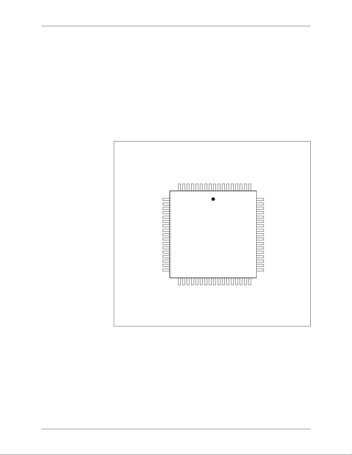
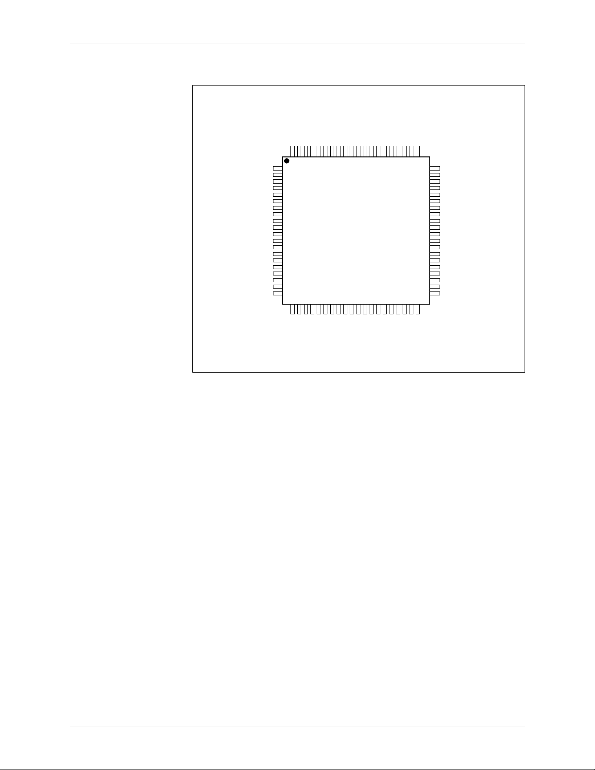
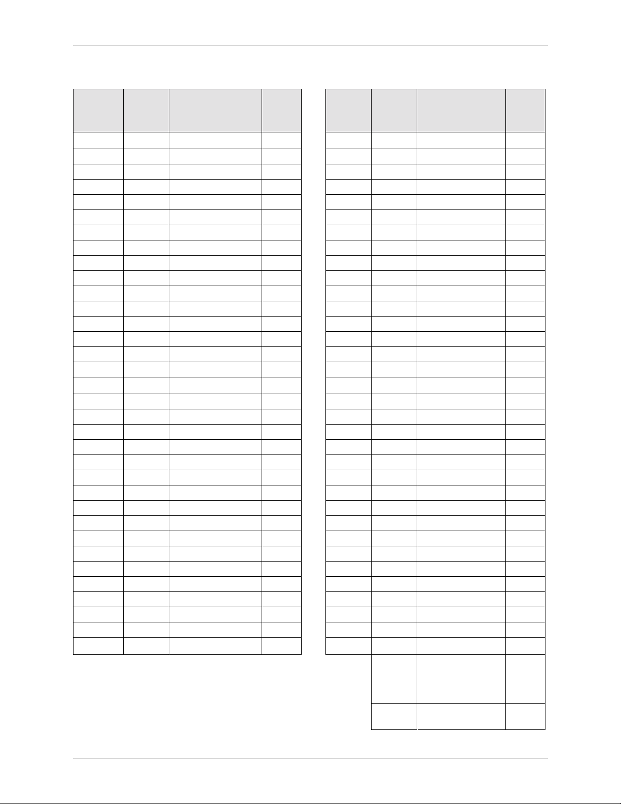
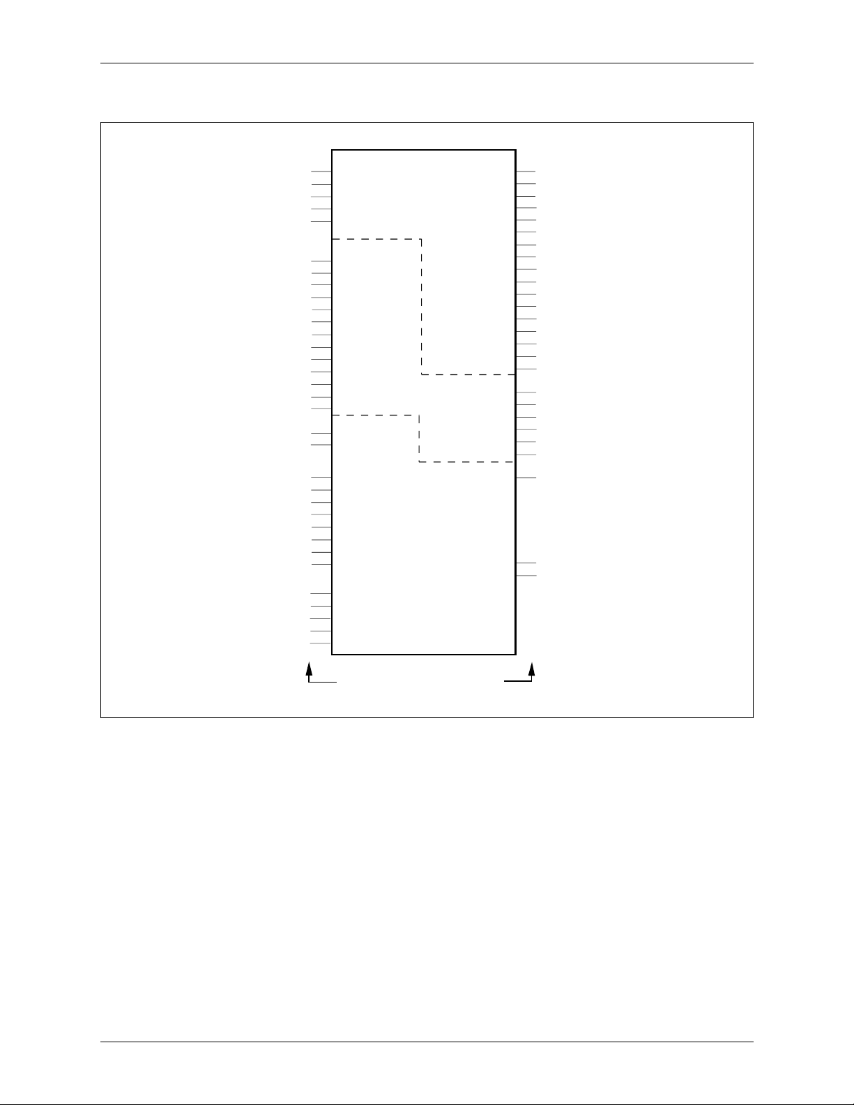
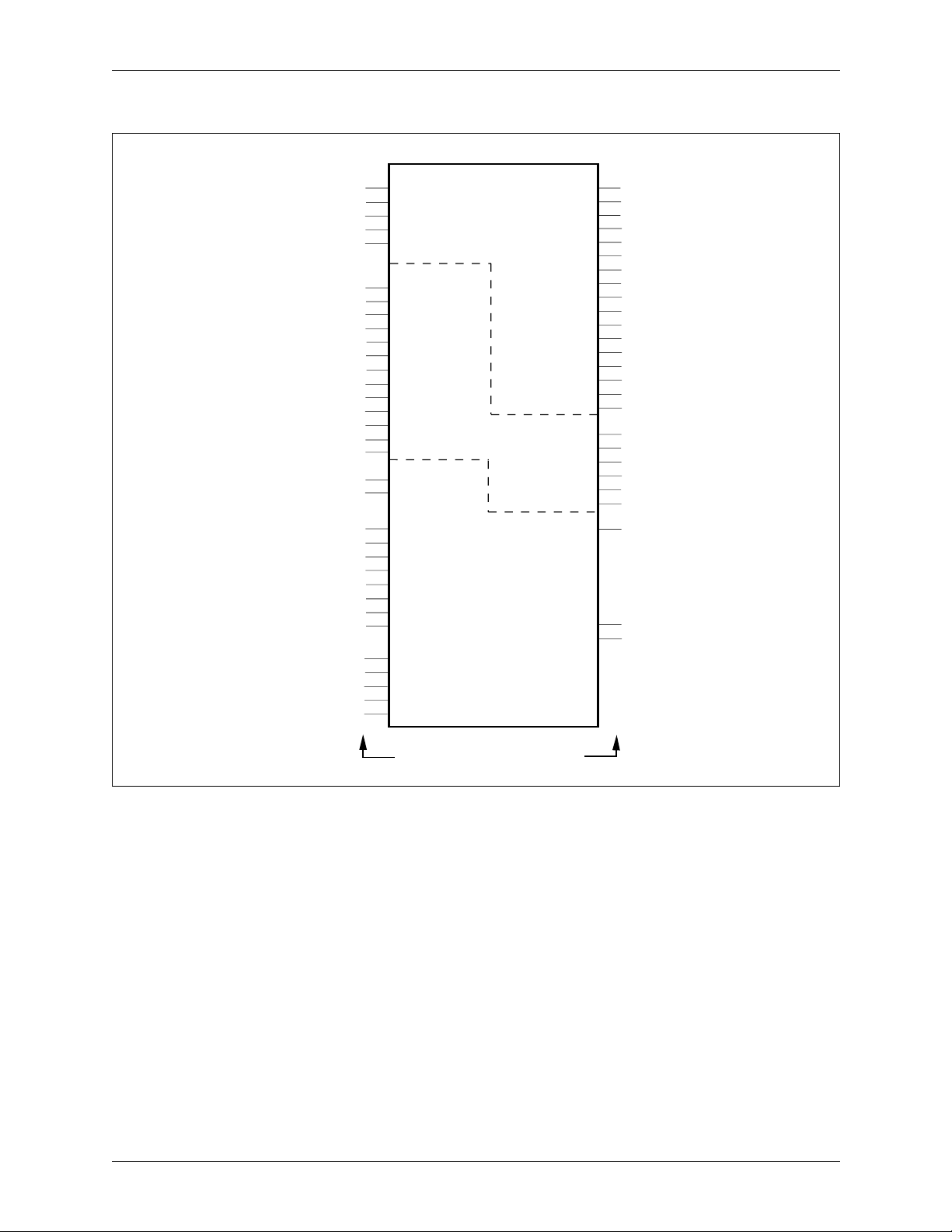
The CN8330 Framer is pa ckaged i n a 6 8-pin Plastic L eaded Chip Carrier (PLCC)
and an 80-pin Metric Quad Flat Pack (MQFP) and shown in Figure 1-1 and
Figure 1-2 respectively. Pin assignments are listed in numerical order in
Table 1-1. Figure 1-3 and Figure 1-4 illustrate functionally partitioned logic
diagrams of the CN8330. Pin descriptions, labels, and I/O assignments are
detailed in Table 1-2.
Figure 1-1. CN8330 Pinout Diagram - 68-Pin PLCC
RXPOS
RXNEG
DS3CKI
TCLKO
RXDAT
RXMSY
RXBCK/RXGAPCK
RXCLK
IDLE/FRMCAR
VALFCS/TXOVH
GND
FIFEN
VCO
RXCKI
V
INIT*
GND
1.1 Pin Descriptions
AD[0]/LOS
AD[1]/OOF
AD[2]/AIS
AD[3]/YEL
AD[4]/IDLE
AD[5]/PAR
987654321
10
11
12
13
14
15
16
17
DD
18
19
20
21
22
23
24
25
26
2728293031323334353637383940414243
AD[6]/LCV
AD[7]/FRMERR
GND
CN8330
Framer
DD
V
ALE/PAREN
WR*CRC32
RD*/ALM1
CS/ALM0
DLINT/SOURCELB
68676665546362
CNTINT/LINELB
MON/MIC*
61
60
TESTI
59
TXSYO
58
TXCKI
57
TXBCK/TXGAPCK
56
TDAT[7]/TXSYI
55
TDAT[6]/TXDATI
54
TDAT[5]/TXENCI
53
TDAT[4]/LCVERRI
52
GND
51
V
DD
50
TDAT[3]
49
TDAT[2]
48
TDAT[1]
47
TDAT[0]
46
TXCCK
45
CBITI
44
PPDLONLY
VDD
GND
RDAT[2]/AID
RDAT[0]/LOS
RDAT[1]/OOF
RDAT[3]/IDLE
RDAT[4]/FRMERR
RDAT/LCVCAR
RDAT[7]TXNRZ
RDAT[6]/RXOVH
CBITO
TESTO
TXPOS
TXNEG
SNDMSG
RXCCK/TXNRZ
SNDFCS
100441E Conexant 1-3
Page 14
1.0 Product Description CN8330
1.1 Pin Descriptions DS3/E3 Framer with 52 Mbps HDLC Controller
Figure 1-2. CN8330 Pinout Diagram - 80-Pin MQFP
AD0/LOS
AD1/OOF
AD2/AIS
AD3/YEL
AD4/IDLE
AD5/PAR
AD6/LCV
AD7/FRMERR
GND
GND
VDDALE/PAREN
W*/CRC32
RD*/ALM1
CS/ALMO
DLINT/SOURCELB
CNTINT/LINELB
MON/MIC*NCNC
GND
FIFEN
VCO
RXPOS
RXNEG
DS3CKI
RXCKI
V
TCLKO
INIT*
RXDAT
RXMSY
RXCLK
RXBCK/RXGAPCK
IDLE/FRMCAR
VALFCS/TXOVH
GND
GND
80797877767574737271706968676665646362
1
NC
2
3
4
5
6
7
8
9
DD
10
11
12
13
14
15
16
17
18
19
20
NC
21222324252627282930313233343536373839
NC
RDAT0/LOS
RDAT1/OOF
RDAT2/AIS
RDAT3/IDLE
CN8330
Framer
RDAT7/TXNRZ
RDAT6/RXOVH
RDAT5/LCVCAR
RDAT4/FRMERR
DD
V
GND
GND
CBITO
TXNEG
RXCCK/TXNRZ
TESTO
TXPOS
61
60
59
58
57
56
55
54
53
52
51
50
49
48
47
46
45
44
43
42
41
40
NC
SNDFCS
SNDMSG
NC
NC
TESTI
TXSYO
TXCKI
TXVBCK/TXGAPCK
TDAT[7]/TXSYI
TDAT[6]/TXDATI
TDAT[5]/TXENCI
TDAT[4]/LCVERRI
GND
GND
V
DD
TDAT3
TDAT2
TDAT1
TDAT0
TXCCK
CBITI
PPDLONLY
8330_002
1-4 Conexant 100441E
Page 15
CN8330 1.0 Product Description
DS3/E3 Framer with 52 Mbps HDLC Controller
1.1 Pin Descriptions
Table 1-1. Pin Descriptions
Pin
(68-Pin
PLCC)
1 72 GND I 35 30 V
2 73 AD[7]/FRMERR B/O 36 31 GND I
3 74 AD[6]/LCV B/O 37 33 CBITO O
4 75 AD[5]/PAR B/O 38 34 RXCCK/TXNRZ O
5 76 AD[4]/IDLE B/O 39 35 TXNEG O
6 77 AD[3]YEL B/O 40 36 TXPOS O
7 78 AD[2]/AIS B/O 41 37 TESTO O
8 79 AD[1]/OOF B/O 42 38 SNDMSG I
9 80 AD[0]/LOS B/O 43 39 SNDFCS I
10 2 GND I 44 41 PPDLONLY I
11 3 FIFEN I 45 42 CBITI I
12 4 VCO O 46 43 TXCCK O
13 5 RXPOS I 47 44 TDAT[0] I
14 6 RXNEG I 48 45 TDAT[1] I
15 7 DS3CKI I 49 46 TDAT[2] I
16 8 RXCKI I 50 47 TDAT[3] I
17 9 V
18 10 TCLKO O 52 49 GND I
19 11 INIT* I 53 51 TDAT[4]/LCVERRI I
20 12 RXDAT O 54 52 TDAT[5]/TXENCI I
21 13 RXMSY O 55 53 TDAT[6]/TXDATI I
22 14 RXCLK O 56 54 TDAT[7]/TXSYI I
23 15 RXBCK/RXGAPCK O 57 55 TXBCK/TXGAPCK O
24 16 IDLE/FRMCAR O 58 56 TXCKI I
25 17 VALFCS/TXOVH O 59 57 TXSYO O
26 18 GND I 60 58 TESTI I
27 22 RDAT[0]/LOS O 61 63 MON/MIC* I
28 23 RDAT[1]/OOF O 62 64 CNTINT/LINELB O/I
29 24 RDAT[2]/AIS O 63 65 DLINT/SOURCELB O/I
30 25 RDAT[3]/IDLE O 64 66 CS/ALM0 I
31 26 RDAT[4]/FRMERR O 65 67 RD*/ALM1 I
32 27 RDAT[5]/LCVCAR O 66 68 WR*/CRC32 I
33 28 RDAT[6]/RXOVH O 67 69 ALE/PAREN I
34 29 RDAT[7]/TXNRZ O 68 70 V
Pin
(80-Pin
MQFP)
Pin Label I/O
DD
Pin
(68-Pin
PLCC)
I5148VDDI
Pin
(80-Pin
MQFP)
1,20,
21,40,
59,60,
61,62
19,32,
50,71
Pin Label I/O
DD
DD
N/C –
GND I
I
I
100441E Conexant 1-5
Page 16
1.0 Product Description CN8330
1.1 Pin Descriptions DS3/E3 Framer with 52 Mbps HDLC Controller
Figure 1-3. CN 8330 Framer Fun ctional Logic Di agram - 68-Pin PLCC
Rx Bipolar Pos
Rx Bipolar Neg
Rx Line Clock In
Dejittered Clock In
FIFO Enable
Tx Clock In
Tx C/N Bit Serial In
Tx Data Bit MSB/Tx M-Sync In
Tx Data Bit 6/Tx Serial Data In
Tx Data Bit 5/Tx Encoder In
Tx Data Bit 4/LCV Error In
Tx Data Bit 3
Tx Data Bit 2
Tx Data Bit 1
Tx Data Bit LSB
Send FCS
Send Message
Parallel Data Only Select
Test In
InitializationII
Address-Data 0/Loss of Signal
Address-Data 1/Out of Frame
Address-Data 2/Alarm Indication Signal
Address-Data 3/Yellow Alarm Detect
Address-Data 4/Idle Code Detection
Address-Data 5/Parity Error Detect
Address-Data 6/Line Code Violation
Address-Data 7/Frame Bit Error
Address Latch Enable/Parallel Input Enable
Chip Select/Alarm 0
Read*/Alarm 1
Write*/Cycle Redundancy Check 32
Monitor/Microprocessor*
B/O
B/O
B/O
B/O
B/O
B/O
B/O
B/O
13
I
RXPOS
14
I
RXNEG
15
I
DS3CKI
16
I
RXCKI
11
I
FIFEN
58
TXCKI
I
45
CBITI
I
56
TDAT[7]/TXSYI
I
55
TDAT[6]/TXDATI
I
54
TDAT[5]/TXENCI
I
53
TDAT[4]/LCVERRI
I
50
TDAT[3]
I
49
TDAT[2]
I
48
TDAT[1]
I
47
TDAT[0]
I
43
SNDFCS
I
42
SNDMSG
I
44
PPDLONLY
I
60
TESTI
19
INIT*
9
AD[0]/LOS
8
AD[1]/OOF
7
AD[2]/AIS
6
AD[3]/YEL
5
AD[4]/IDLE
4
AD[5]/PAR
3
AD[6]/LCV
2
AD[7]/FRMERR
67
I
ALE/PAREN
64
I
CS/ALM0
65
I
RD*/ALM1
66
I
WR*/CRC32
61
I
MON/MIC*
Receiver
Section
RDAT[7]/TXNRZ
RDAT[6]/RXOVH
RDAT[5]/LCVCAR
RDAT[4]/FRMERR
VALFCS/TXOVH
RXBCK/RXGAPCK
TXBCK/TXGAPCK
Transmitter
Section
Microprocessor
Interface
CNTINT/LINELB
DLINT/SOURCELB
RXDAT
RXMSY
RXCLK
CBITO
RXCCK/TXNRZ
RDAT[3]/IDLE
RDAT[2]/AIS
RDAT[1]/OOF
RDAT[0]/LOS
IDLE/FRMCAR
VCO
TXCCK
TXPOS
TXNEG
TXSYO
TCLKO
TESTO
Rx Serial Data
20
O
Rx M-Sync
21
O
Rx Clock
22
O
Rx C/N Bit Serial Out
37
O
Rx C/N-Bit Clock Out/TxNRZ
38
O
Rx Data Bit MSB/TxNRZ
34
O
Rx Data Bit 6/RX Overhead
33
O
Rx Data Bit 5/ Line Code Violation Carry
32
O
Rx Data Bit 4/Frame Bit Error
31
O
Rx Data Bit 3/Idle Code Detection
30
O
Rx Data Bit 2/Alarm Indication Signal
29
O
Rx Data Bit 1/Out of Frame
28
O
Rx Data Bit LSB/Loss of Signal
27
O
Idle Data Rcvd/Frame Carry
24
O
Valid FCS Rcvd/TX Overhead
25
O
Voltage-Controlled Oscillator Output
12
O
Rx Byte Clock/Gapped Clock
23
O
Tx Byte Clock/Gapped Clock
57
O
Tx C/N Bit Clock
46
O
Tx Bipolar Pos
40
O
Tx Bipolar Neg
39
O
Tx M-Sync Out
59
O
Tx Clock Out
18
O
41
Test Out
O
62
Counter Interrupt/Line Loopback
O/I
63
Data Link Interrupt/Source Loopback
O/I
B = Bidirectional, I = Input, O = Output
1-6 Conexant 100441E
Page 17
CN8330 1.0 Product Description
DS3/E3 Framer with 52 Mbps HDLC Controller
Figure 1-4. CN 8330 Framer Fun ctional Logic Di agram - 80-Pin MQ FP
B/O
B/O
B/O
B/O
B/O
B/O
B/O
B/O
5
I
RXPOS
6
I
RXNEG
7
I
DS3CKI
8
I
RXCKI
3
I
FIFEN
56
TXCKI
I
42
CBITI
I
54
TDAT[7]/TXSYI
I
53
TDAT[6]/TXDATI
I
52
TDAT[5]/TXENCI
I
51
TDAT[4]/LCVERRI
I
47
TDAT[3]
I
46
TDAT[2]
I
45
TDAT[1]
I
44
TDAT[0]
I
39
SNDFCS
I
38
SNDMSG
I
41
PPDLONLY
I
58
TESTI
11
INIT*
80
AD[0]/LOS
79
AD[1]/OOF
78
AD[2]/AIS
77
AD[3]/YEL
76
AD[4]/IDLE
75
AD[5]/PAR
74
AD[6]/LCV
73
AD[7]/FRMERR
69
I
ALE/PAREN
66
I
CS/ALM0
67
I
RD*/ALM1
68
I
WR*/CRC32
63
I
MON/MIC*
Receiver
Section
RDAT[7]/TXNRZ
RDAT[6]/RXOVH
RDAT[5]/LCVCAR
RDAT[4]/FRMERR
VALFCS/TXOVH
RXBCK/RXGAPCK
TXBCK/TXGAPCK
Transmitter
Section
Microprocessor
Interface
CNTINT/LINELB
DLINT/SOURCELB
RXCCK/TXNRZ
Rx Bipolar Pos
Rx Bipolar Neg
Rx Line Clock In
Dejittered Clock In
FIFO Enable
Tx Clock In
Tx C/N Bit Serial In
Tx Data Bit MSB/Tx M-Sync In
Tx Data Bit 6/Tx Serial Data In
Tx Data Bit 5/Tx Encoder In
Tx Data Bit 4/LCV Error In
Tx Data Bit 3
Tx Data Bit 2
Tx Data Bit 1
Tx Data Bit LSB
Send FCS
Send Message
Parallel Data Only Select
Test In
InitializationII
Address-Data 0/Loss of Signal
Address-Data 1/Out of Frame
Address-Data 2/Alarm Indication Signal
Address-Data 3/Yellow Alarm Detect
Address-Data 4/Idle Code Detection
Address-Data 5/Parity Error Detect
Address-Data 6/Line Code Violation
Address-Data 7/Frame Bit Error
Address Latch Enable/Parallel Input Enable
Chip Select/Alarm 0
Read*/Alarm 1
Write*/Cycle Redundancy Check 32
Monitor/Microprocessor*
RXDAT
RXMSY
RXCLK
CBITO
RDAT[3]/IDLE
RDAT[2]/AIS
RDAT[1]/OOF
RDAT[0]/LOS
IDLE/FRMCAR
VCO
TXCCK
TXPOS
TXNEG
TXSYO
TCLKO
TESTO
1.1 Pin Descriptions
Rx Serial Data
12
O
Rx M-Sync
13
O
Rx Clock
14
O
Rx C/N Bit Serial Out
33
O
Rx C/N-Bit Clock Out/TxNRZ
34
O
Rx Data Bit MSB/TxNRZ
29
O
Rx Data Bit 6/RX Overhead
28
O
Rx Data Bit 5/ Line Code Violation Carry
27
O
Rx Data Bit 4/Frame Bit Error
26
O
Rx Data Bit 3/Idle Code Detection
25
O
Rx Data Bit 2/Alarm Indication Signal
24
O
Rx Data Bit 1/Out of Frame
23
O
Rx Data Bit LSB/Loss of Signal
22
O
Idle Data Rcvd/Frame Carry
16
O
Valid FCS Rcvd/TX Overhead
17
O
Voltage-Controlled Oscillator Output
4
O
Rx Byte Clock/Gapped Clock
15
O
Tx Byte Clock/Gapped Clock
55
O
Tx C/N Bit Clock
43
O
Tx Bipolar Pos
36
O
Tx Bipolar Neg
35
O
Tx M-Sync Out
57
O
Tx Clock Out
10
O
37
Test Out
O
64
Counter Interrupt/Line Loopback
O/I
65
Data Link Interrupt/Source Loopback
O/I
B = Bidirectional, I = Input, O = Output
100441E Conexant 1-7
Page 18

1.0 Product Description CN8330
1.1 Pin Descriptions DS3/E3 Framer with 52 Mbps HDLC Controller
Table 1-2. Hardware Signal Definitions (1 of 5)
Pin Label Signal Name I/O Definition
ALE/PAREN Address L a tch
Enable/Parallel Input Enable
I A dual-purpose active-high signal which, when
MON/MIC* is tied low, is microprocessor-generated
and causes the CN8330 to latch in the address on
the address-data bus. When MON/MIC* is tied high
(stand-alone mode), the parallel input for the PPDL
formatter is e nabled. When this pin is tied low,
transmit data is sourced from the serial input
TDAT[6]/TXDAT.
(1)
CS/ALM0 C hip Select/Alarm 0 I A dual-purpose signal that enabl es read/write
functions when MON/MIC* is tied low, and controls
AIS transmission in stand-alone mode when
MON/MIC* is tied high. Both CS and ALM0 are
active high signals.
(1)
RD*/ALM1 Read/Alarm 1 I A dual-purpose signal tha t en ables read data to be
passed to the address-data bus when MON/MIC* is
tied low, and controls idle code tr ansmission in
stand-alone mode when MON/MIC* is tied high,
WR*/CRC32 Write/Cycle Redundancy
Check 32
RD* is an active low signal and ALM1 is
active-high.
I A dual-purpose signal t hat latches write data from
the address-data bus when MON /MIC* is tied low,
(1)
and controls the Cycle Redundancy Check (CRC)
when MON/MIC* is tied high. WR* is an active low
signal. In stand-alone mode, a high-speed 32-bit
CRC calculation is enabled if CRC32 is high; if low, a
16-bit calculation is performed.
(1)
MON/MIC* Monitor/Microprocessor
Microprocessor Interface
Mode Select
AD[0]/LOS A ddress-Data 0/Loss of
Signal
I Selects either microprocessor mode when tied low,
or stand-alone monitor mode when tied high. The
state of MON/MIC* determines which function the
dual-purpose pin s (AD[7:0]) serve. The standalone
mode is valid only in DS3 mode.
(1)
B/O Part of the bidirectional 8-bit multiplexed
address-data bus when MON/MIC* is tied low. When
in stand-al one mode, this pin is an active-hig h
monitor output ind ic a t in g los s of si gn al.
(1)
AD[1]/OOF Address-Data 1/Out of Frame B /O Part of the bidirectional 8-bit multiplexed
address-data bus when MON/MIC* is tied low. When
AD[2]/AIS Address-Data 2/Alarm
Indication Signal
in stand-al one mode, this pin is an active-hig h
monitor output indicating an out-of-frame state.
B/O Part of the bidirectional 8-bit multiplexed
address-data bus when MON/MIC* is tied low. When
(1)
in stand-al one mode, this pin is an active-hig h
AD[3]/YEL Address-Data 3/Yellow Alarm
Detection
monitor output indicating alarm indication signal
detection.
B/O Part of the bidirectional 8-bit multiplexed
address-data bus when MON/MIC* is tied low. When
in stand-al one mode, this pin is an active-hig h
monitor output indicati ng a yellow alarm.
(1)
(1)
1-8 Conexant 100441E
Page 19

CN8330 1.0 Product Description
DS3/E3 Framer with 52 Mbps HDLC Controller
Table 1-2. Hardware Signal Definitions (2 of 5)
Pin Label Signal Name I/O Definition
AD[4]/IDLE Addr ess-Data 4/Idle Code
Detection
AD[5]/PAR Address-Data 5/Parity Error
Detection
AD[6]/LCV Address-Data 6/L ine Code
Violation
AD[7]/FRMERR Address-Data 7/
Frame Bit Error
CNTINT/LINELB Counter Interrupt/
Line Loopback
Microprocessor Interface
DLINT/SOURCELB Data Link Interrupt/Source
Loopback
1.1 Pin Descriptions
B/O Part of the bidirectional 8-bit multiplexed
address-data bus when MON/MIC* is tied low. When
in stand-al one mode, this pin is an active-hig h
monitor output ind ic a tin g an idl e co d e de tec t io n.
(1)
B/O Part of the bidirectional 8-bit multiplexed
address-data bus when MON/MIC* is tied low. When
in stand-al one mode, this pin is an active-hig h
monitor output indicating a parity error.
(1)
B/O Part of the bidirectional 8-bit multiplexed
address-data bus when MON/MIC* is tied low. When
in stand-al one mode, this pin is an active-hig h
monitor output indicating a line code violation.
(1)
B/O Part of the bidirectional 8-bit multiplexed
address-data bus when MON/MIC* is tied low. When
in stand-al one mode, this pin is an active-hig h
monitor output ind ic at in g a fram e bi t err or.
(1)
O/I The composite int e rrupt signal gener a ted by the
error counters when MON/MIC* is tied low. When
MON/MIC* is tied high, this pin controls line
loopback transmission in stand-alone mode. CNTINT
is an active-low output; LIN ELB is an active-high
input.
O/I The composite interru pt signa l gene rated by the data
links when MON/MIC* is tied low. When MON/MIC*
is tied high, this pin controls source loopback
transmission in stand- alone mode. DLINT is an
active-low output; SOURCELB is an active-high
input.
TESTI Test In I Used for test functions only. Should be tied to
ground for normal operation.
INIT* Initialization I Active low initialization control. Not all internal
storage elements are affected by t his signal. See
Clock Interfac e and Initialization in th e Overview
section of the Functional Description chapter.
TESTO Test Out O Used for test functions only. Should be left
disconnected for normal operation.
100441E Conexant 1-9
Page 20

1.0 Product Description CN8330
1.1 Pin Descriptions DS3/E3 Framer with 52 Mbps HDLC Controller
Table 1-2. Hardware Signal Definitions (3 of 5)
Pin Label Signal Name I/O Definition
TCLKO Transmit Clock Out O Used to clock out the TXP OS and TXNEG output s.
Data is clocked out on the rising edge of TCLKO.
TXPOS, TXNEG Transmit Bipolar
Positive, Negative
TDAT [3:0] Transmit Data Bits 3–0 (Bi t 0
is the LSB)
TDAT[4]/LCVERRI Transmit Data Bit 4/Line
Code Violation Error In
TDAT[5]/TXENCI Transmit Data Bit 5/Transmit
Transmitter Section
TDAT[6]/T XDATI Transmit Data Bit 6/Transmit
TDAT[ 7]/TXS YI Transmit Data Bit7/Transmit
Encoder In
Serial Data
M-Sync In
O The positive and negative pulses generat ed by the
B3ZS/HDB3 encode r.
I In parallel mode
of the byte-oriented data that is input to the PPDL
transmitter in response to the transmit byte c lock,
TXBCK.
I In parallel mode, the TDAT[4] is bit 4 of the
byte-oriented data that is input to the PPDL
transmitter. In serial mode, LCVERRI allows test
equipment to insert LCVs into the transmit stream
under microprocessor control, in both DS3 and E3
modes.
I In parallel mode , TDAT[5] is bit 5 of the
byte-oriented data that is input to the PPDL
transmitter. In serial mode, TXENCI is an alternate
direct input to t he B3ZS/HDB3 enc oder.
I In parallel mode , TDAT[6] is bit 6 of the
byte-oriented data that is input to the PPDL
transmitter. In serial mode, TXDATI is applied to the
transmitter.
I In parallel mode, TDAT[7] is the MSB (Bit 7)of the
byte-oriented data that is input to the PPDL
transmitter. In serial mode, TXSYI is applied to the
transmitter.
(2)
, these bits form the lower nibble
TXSYO Transmit M-Sync Out O The transmit M-frame sync output.
TXCKI Transmit Clock In I TXCKI rising edge is used to sample parallel data,
TXBCK/TXGAPCK Transmit Byte Clock/Gapp e d
Clock
SNDMSG Send Message I In parallel mode, SNDMSG initiates message
SNDFCS Send Frame Check Sequence I In parallel mode, SNDFCS initiates transmission of
Transmitter Section
CBITI Tra nsm it C/N-B it Seria l In I The serial C-bit (DS3 m ode ) o r N - bi t (E 3 m ode) d ata
TXCCK Transmit C/N-Bit Clock O Used to sample the CBITI input on the falling edge of
PPDLONLY Payload Parallel Data Only
Select
while the falling edge is used to sample serial dat a.
O In parallel mode, TXBCK clocks the by te-oriented
data that is input to the PPDL transmitter. In serial
mode, TXGAPCK is a transmit clock that is gapped
during overhead bit intervals in either E3 or DS 3
modes.
transmission in the PPDL transmitter.
the 16- or 32-bit frame check sequence on the PPDC
transmitter.
input to be transmitted.
TXCCK.
I Enables the PPDL- only mode in which no DS3/E3
framing is inserted. This mode is entered by tying
this pin high.
1-10 Conexant 100441E
Page 21

CN8330 1.0 Product Description
DS3/E3 Framer with 52 Mbps HDLC Controller
Table 1-2. Hardware Signal Definitions (4 of 5)
Pin Label Signal Name I/O Definition
DS3CKI DS3 Receive Line Clock In I Clock input DS3CKI should be connected to a 44.736
RXPOS, RXNEG Receive Bipolar
Positive/Negative
RXCKI Receive Dejittered
Clock In
FIFEN FIFO Enable I An active-high input whi ch enables the internal
RXDAT Receive Serial Data O RXDAT is the serial data bit stream clocked out on
RXMSY Receive M-Sync O The M-frame synchronization output recovered from
1.1 Pin Descriptions
MHz source (34.368 MHz for the E3) derived from
incoming receive data.
I The input positive and negative pulses are sampled
on the rising edge of the receiver input clock
(DS3CKI) and should be a full clock period wide.
I Used to read the received data out of the internal
FIFO (required only if FIFO is enabled). If unused, tie
to ground.
FIFO, used to dejitter the received data by using the
dejittered clock input, RXCKI. When FIFEN is low, the
FIFO is bypassed and the serial data is output with
respect to the incoming clock, DS3CKI.
the rising edge of RXCLK.
the incoming serial data stream.
RXCLK Receive Clock O The receive clock used internally to clock out the
serial data stream onto RXDAT.
RXBCK/RXGAPC K Receive Byte/Gapped Clock O When in serial m ode, RXGAPCK provides a gapped
clock signal during every overhead bit (in both DS3
Receiver Section
CBITO Receive C/N-Bit Serial Ou t O The receive serial C-bit (DS3 mode) or N-bit (E3
RXCCK/TXNRZ Receive C/N-Bit Clock
Out/Transmit NRZ
RDAT[0]/LOS Receive Data Byte 0/Loss of
Signal
RDAT[1]/OOF Receive Data Byte 1/
Out of Frame
RDAT[2]/AIS Receive Data Byte 2/Alarm
Indication Signal
and E3 modes). In parallel mode, RXBCK is used to
internally clock out the receive byte-oriented data on
RDAT[7:0].
mode) data. CBITO changes on the rising edge of
RXCCK.
O A clock that indicates transitions in the CBIT0 signal.
In PPDL-only mode, tran smit NRZ data is availa ble
on this pin.
O Part of the 8-bit data bus output from the PPDL
receiver when parallel mode is enabled. When
parallel mode is disabled, this pin is an active-high
monitor output ind ic a t in g los s of si gn al.
O Part of the 8-bit data bus output from the PPDL
receiver when parallel mode is enabled. When
parallel mode is disabled, this pin is an active-high
monitor output indic a ting out-of-frame.
O Part of the 8-bit data bus output from the PPDL
receiver when parallel mode is enabled. When
parallel mode is disabled, this pin is an active-high
monitor output indicating alarm indication signal.
100441E Conexant 1-11
Page 22

1.0 Product Description CN8330
1.1 Pin Descriptions DS3/E3 Framer with 52 Mbps HDLC Controller
Table 1-2. Hardware Signal Definitions (5 of 5)
Pin Label Signal Name I/O Definition
RDAT[3]/IDLE Receive Data Byte 3/Idle
Code Detection
RDAT[4]/
FRMERR
RDAT[5]/
LCVCAR
Receive Data Byte 4/F r ame
Error Detection
Receive Data Byte 5/Line
Code Violation Carry
RDAT[6]/RXOVH Receive Data Byte 6/Receive
Overhead Detection
RDAT[7]/TXNRZ Receive Data Byte 7/ Trans-
Receiver Section
IDLE/
mit NRZ Out
Idle/Frame Carry O Set if an idle flag is received after a non-idle
FRMCAR
O Part of the 8-bit data bus output from the PPDL
receiver when parallel mode is enabled. When
parallel mode is disabled, this pin is an active-high
monitor output indicating idle code detection.
O Part of the 8-bit data bus output from the PPDL
receiver when parallel mode is enabled. When
parallel mode is disabled, this pin is an active-high
monitor output indicating frame error detection.
O Part of the 8-bit data bus output from the PPDL
receiver when parallel mode is enabled. When
parallel mode is disabled, this pin is an active-high
ripple carry output from the LCV error counter.
O Part of the 8-bit data bus output from the PPDL
receiver when parallel mode is enabled. When
parallel mode is disabled, this pin is an active-low
monitor output indicating the receive overhead bit
positions.
O Part of the 8-bit data bus output from the PPDL
receiver when parallel mode is enabled. When
parallel mode is disabled, this pin is a monitor
output for the transmit NRZ data.
sequence, when parallel mode is enabled. When
parallel mode is disabled, this pin is an active-high
ripple carry output from the frame error counter.
VALFCS/TXOVH Valid FCS Received/Transmit
Overhead
O Active high if a valid FCS was received, when parallel
mode is enabled. Wh en parallel mode is disabled,
this pin is an active-low t r ansmit overhead bit
position indicator.
VCO Voltage-Controlled Os cillator
Output
O Used as the phase control for the clock recovery
circuit that generates the dejittered clock, RXCKI.
Valid only when FIFEN is high. FIFEN enables the
internal FIFO when tied high.
V
DD
Supply Voltage Four pins are provided for power.
GND Ground Five pins are provided for ground.
VCC and GND
NC Not Connected These pins are not connected internally.
Not Connected
NOTE(S):
(1)
Standalone operation is valid only in DS3 mode.
(2)
Parallel mode is enabled by setting the Parallel Data Enable bit [ParaEn;CR04.3] in the Feature Control Register [CR04; 0x04]
when MON/MIC* is low. When MON/MIC* is high, Parallel mode is entered by tying the ALE/PAREN pin high .
1-12 Conexant 100441E
Page 23

2.0 Functional Description
2.1 Overview
2.1.1 Brief Block Description
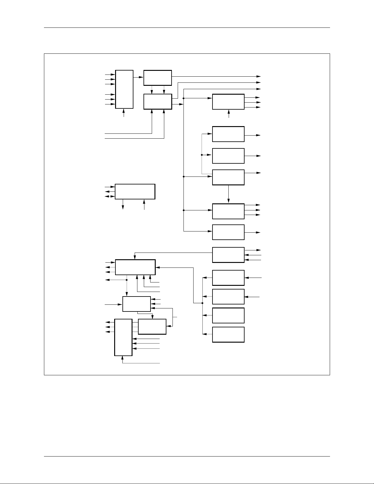
A block diagram of the circuit is illustrated in Figure 2-1. The receive
B3ZS/HDB3 signal is decoded and the bipolar input is converted to a unipolar,
clocked serial data stream. Frame bit conten t is checked and the overhead bit data
links and alarms are extrac ted. The recei v e clock is pro vi ded at the receiv er outp ut
(RXCLK). The data is also connected to a Payload Parallel Data Link (PPDL)
receiver that decodes message blocks using the High-Level Data Link Control
(HDLC) format (Refer to Appendix A in this document for a description of the
HDLC formatter). The recovered data bytes are provided on a parallel output port
with a byte clock. The PPDL receiver can also be programmed to operate in
nibble mode or transparently without HDLC formatting.
A First In First Out (FIFO) memory buffer in the rece ive signal path c an be
enabled to reduce the jitter on t he incomi ng d ata . The receive data is clocked into
the FIFO buffer after bipolar decoding. The FIFO buffer provides a Voltage
Controlled Oscillator (VCO) control signal to an external clock recovery circuit.
A dejittered clock (RXCKI) from the VCO is then used to read the data from the
FIFO buffer to the remainin g receiver circuitry.
The transmitter is capable of sending either serial data from an ext ernal pin, or
byte- or nibble-oriented data from the PPDL data port. DS3 overhead bits or E3
Frame Alignment Signal (FAS) bits are automatically inser ted. Parallel data can
be formatted with idle flags, zero stuf fing for transparency, and a selectable 16- or
32-bit Frame Check Sequ ence (FCS). Bytes or nibbles without HDLC formatting
can also be transmitted. The transmitter is able to send AIS, idle code, yellow
alarm, and all-ones signals. DS3 C-bits (or E3 N-bits) can be optionally inserted
into the data stream from an external source.
LAPD (Link Access Procedure-D) receiver and transmitter circuitry is
provid ed for the terminal data link in DS3 C -bit par ity format and t he E3 mod e. In
C-bit mode, the three C-bits in subframe 5 of the M-frame are used for the
terminal data lin k. In E3 mode, the N-bit is used for the terminal data link.
The microprocessor interface or external outputs monitors all status
indications in the received signal. For both DS3 and E3 modes, indications
include AIS, all-ones, and yellow alarm detection; and Out-of-Frame (OOF) and
frame bit error counting. In addition, loss of signal, idle code, and parity error
detection; line code violation (LCV), path parity, and FEBE event counting; and
parity and X-bit disagreement counting are pro vided for DS3 mode. The recei v ed
DS3 C-bits (or E3 N-bits) are available on an external pin to provide visibility for
external processing, if necessary.
2
100441E Conexant 2-1
Page 24
2.0 Functional Description CN8330
2.1 Overview DS3/E3 Framer with 52 Mbps HDLC Controller
Figure 2-1. Functional Block Diagram
Receive
RXPOS
RXNEG
DS3CKI
TXPOS
TXNEG
TXCKI
MUX
SOURCELB
Conversion
CLK
Unipolar
FIFO
Buffer
DATA
PPDL
Receiver
Rx Timing
LOS, LCV
VCO
RXDAT, RXCLK
RXBCK
RDAT[7:0]
Status: IDLE
VALFCS
RXCKI
FIFEN
Control
Interrupts
Address/Data
CBITI
TXCCK
TXSYO
TXNRZ Data
FIFO Data
for Line
Loopback
TXPOS
TXNEG
TCLKO
Microprocessor
Interface
Control
Framing and
Overhead Bit
Insertion
MUX
MUX
Status
Encoding
Receive Clock
Bipolar
and Data
Transmit
TXDATI
TXCKI
TXSYI
TXENCI
LINELB
RXPOS
RXNEG
DS3CKI
Test
Equipment
Feature
Select
FEAC
Channel
Terminal
Data Link
Receiver
Frame/
Overhead
Bit Check
Frame
Recovery
Payload
Bit Check
PPDL
Transmitter
FEAC
Channel
Terminal Data
Link
Generator
Payload Bit
Pattern Insert
FEBE
Generation
Receive Byte
Message Buffer
Status: OOF
Frame Error
Parity
Path Parity
FEBE
X Bit
Format
RXMSY
Gapped Clock
CBITO,RXCCK
Status: AIS
IDLE
TXBCK
TDAT[7:0]
SNDMSG, SNDFCS
Transmit Byte
Message Buffer
LINELB
2-2 Conexant 100441E
Page 25

CN8330 2.0 Functional Description
DS3/E3 Framer with 52 Mbps HDLC Controller
2.1.2 Clock Interface and Initialization
The CN8330 clock input (TXCKI) controls the transmitter. This input should be
supplied with a 44.736 MHz clock in DS3 mode and a 34.368 MHz clock in E3
mode. TDAT[6]/TXDATI is sampled on the falling edge of TXCKI and
TDAT[7]/TXSYI is sampled o n the rising edge of TXCKI. The transmit pulses
TXPOS and TXNEG are clocked out on the rising edge of TCLKO.
DS3CKI is the raw data clock that accomp anies the RXPOS and RXNEG data
pulse inputs for the receiver. If the FIFO buffer is enabled , the data is clocked into
the FIFO buffer after B3ZS/HDB3 decoding. RXCKI is the dejittered version of
DS3CKI and is used to clock the receive data out of the FIFO buffer (if enabled)
to the rest of the receiver circuitry . If the FIFO buffer is disabled, DS3CKI clocks
the data into all of the receiver circuitry and the RXCKI input should be
grounded.
Clock timing requirements are given in the Electrical and Mechanical
Specifications chapter.
2.1.2.1 Initialization The CN8330 can be initialized with an active-low input pulse of at least 200 ns
duration on the INIT* pin. All error counters are initialized to zero when this
input is active low if the transmit and receive clocks are present. Initialization is
not required for proper operation. During initialization (active low) host cannot
read or write any CN8330.
2.1 Overview
2.1.3 Microprocessor Interface
The CN8330 can be controlled by a microprocessor or a microcontroller through
an 8-bit multiplexed address/data interface. An interface to an Intel 8051 family
processor or equivalent, or Motorola 68HC11 family or equivalent is provided.
The microprocessor interface is enabled by tying the MON/MIC* pin low. The
CN8330 is connected to the microprocessor exactly like static RAM.
2.1.3.1 Using with
Specific Microcontrollers
The microprocessor interface i s designed to allow direct connection o f I nt el 8051
family, Motorola 68HC11 family, or equivalent microcontrollers. The controller
interface to the CN8330 consists of 14 pins: Address Latch Enable (ALE), Read
Enable (RD*), Write Enable (WR*), Chip Select (CS ), e ig ht multiplexed
address/data bits (AD[7:0]), and two interrupts (DLINT/SOURCELB and
CNTINT/LINELB). If a 68HC11 controller is used, then its address strobe as is
connected to ALE, Enable is connected to RD*, and Read/Write* (R/W*) is
connected to WR*. The chip select input (CS/ALM0) allows the control of
multiple ICs from a single mi croprocessor. Interrupt outputs are used for data link
and maintenance operations and provide active-low interrupts.
100441E Conexant 2-3
Page 26

2.0 Functional Description CN8330
2.1 Overview DS3/E3 Framer with 52 Mbps HDLC Controller
2.1.3.2 Microprocessor Interrupts
There are two se parat e i nterrupt pins that can be con nected to the microprocessor
(or microcontroller): Counter and Data Link. The counter interrupt pin
(CNTINT/LINELB) combines seven sources of interrupts on an external pin
connected to the microprocessor. This interr upt signal is active low and is a
composite indication of all interrupt sources that are enabled in the Status
Interrupt Control Register [CR02;0x02]. The interrupt source can be determined
by reading the Counter Interrupt Status Register [SR01;0x11]. The data link
interrupt pin (DLINT/SOURCELB) is a composite indic ation of the interrupts
from four sources. The interrupt source can be determined by reading the Data
Link Interrupt Status Register [SR02;0x12]. When the C-Bit P arit y Mode/ E nable
DLINT bit [CBitP/DL;CR00.0] is not set, the DLINT/SOURCELB pin is held
high (inactive). The two interrupt pins are open-drain outputs and can be
connected to form a single-wire ORed interrupt, if desired.
2.1.3.3 Address Map The register addre ss map f or t he CN83 30 i s g iven in T able 3-1 through Table 3-4,
Register Summary. There are three types of registers: Control Registers, which
can be read or written; St atus Re gist ers and Cou nters w hi ch can on l y be r ead; a nd
Data Link Message Buffers which can be read or written. The Control Registers
serve as latches that are modified by a microprocessor write operation and can
also be read to verify contents. They are located at addresses 0x00–0x05. Statu s
Registers are located at addresses 0x10–0x16. Maintenance Error Counters are
located at addresses 0x20–0x26. The Transmit Terminal Data Link Message
Buffers are located at addresses 0x30–0x37, and the Receive Terminal Data Link
Message Buffers are located at addresses 0x40–0x47. The chip select input
(CS/ALM0) must be high to address the CN8330 and to enable read or write
operations.
2-4 Conexant 100441E
Page 27
CN8330 2.0 Functional Description
DS3/E3 Framer with 52 Mbps HDLC Controller
2.2 Line Interfaces
2.2.1 Transmitter Line Interface
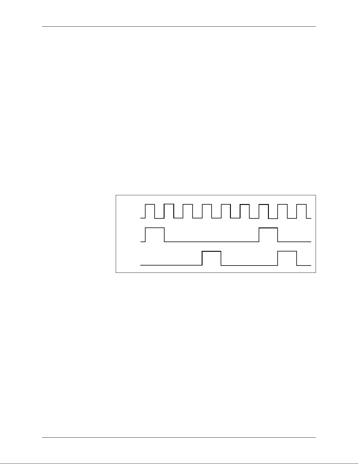
The transmitted line signals are shown in Figure 2-2. Nine bits of a representati ve
output sequence are shown. Separate signal pins provide the appropriate output
signal for positive and negative pulses. The outputs are a full clock period wide
and change on positive clock transitions of the TCLKO pin. For additional
information on the TXPOS and TXNEG output s refer to Transmitter Outputs in
the Transmitter Operation section in this chapter
B3ZS/HDB3 encoding is performed automatically on the output data stream;
however, this encoding can be disabled to send AMI data without any zero code
suppression. Tran smit NRZ data, prior to B3ZS /HDB3 encoding, is also available
on the RDAT[7]/TXNRZ pin when parallel mode is not selected and on the
RXCCK/TXNRZ pin when PPDLONLY mode is selected.
Figure 2-2. Transmitter Line Driver Outputs
2.2 Line Interf aces
TCLKO
TXPOS
TXNEG
100441E Conexant 2-5
Page 28
2.0 Functional Description CN8330
2.2 Line Interfaces DS3/E3 Framer with 52 Mbps HDLC Controller
2.2.2 Receiver Line Interface
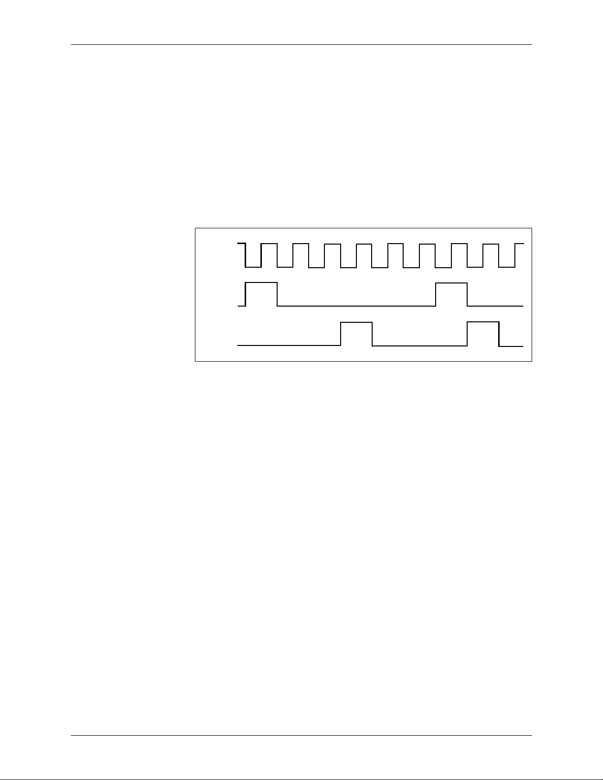
The line interface for the receive bipo lar signals consists of tw o lo gic-lev el signals
that represent the positive and negative bipolar line pulses (RXPOS, RXNEG)
and an input (DS3CKI) for an externally derived clock at a nominal frequency of
44.736 MHz or 34.368 MHz. The receiver line signals are shown in Figure 2-3.
Nine bits of a representative input sequence are shown. The input signal is
sampled on the rising ed ge of t he cloc k signal. B 3ZS/HDB3 deco ding i s provided
internally. Decoding can be defeated for NRZ input s by connecting the NRZ data
input to both the RXPOS an d RXNEG i nputs or b y sel ecting the AMI mo de/LCV
Type 2 bit [AMI/LCV2;CR04.6] in the Feature Control Register [CR04;0x04].
Figure 2-3. Clocked Receiver Input
DS3CKI
RXPOS
RXNEG
2-6 Conexant 100441E
Page 29

CN8330 2.0 Functional Description
DS3/E3 Framer with 52 Mbps HDLC Controller
2.3 Transmitter Operation
The transmitter circuit is synchronized to the transmit input data by an external
synchronization signal. The external synchronization signal sets the M-frame
reference for transmitted signals.
2.3.1 Input and Synchronization
The input to the transmitter consists of the transmit serial data input (or the PPDL
transmitter data), transmit clock, and transmit M-frame sync signal. An M-frame
sync signal output is available on the TXSYO pin to synchronize external
circuitry, if desired. If an input sync is not provided, the CN8330 gener ates a sync
internally whose position is indicated by TXSYO. In this case, the sync input
should be grounded. The TDAT[7]/TXSYI is sampled on the rising edge of
TXCKI and TDAT[6]/TXDATI is sampled by the falling edge of TXCKI.
2.3.2 DS3 Mode
2.3 Transmitter Operation
The input bits are synchronized to the M-frame sync signal, which can either be
externally provided or taken from the M-frame sync signal that is internally
generated. Serial input data on TDAT[6]/TXDATI must contain bit positions for
the ove rhead bits, although these are not used unless external insertion is enabled.
The clock frequency is nominally 44.736 MHz and the transmit data input is
sampled on the falling edge of the clock signal. The path delay of the transmitter
from the serial data in put to the positive and negative outputs is six cycles of the
transmit clock. This delay includes B3ZS/HDB3 coding. The delay from the
serial data input to t he NRZ o utput is t w o clock c ycles a nd the co ding delay of the
B3ZS encoder is four clock cycles.
100441E Conexant 2-7
Page 30
2.0 Functional Description CN8330
2.3 Transmitter Operation DS3/E3 Framer with 52 Mbps HDLC Controller
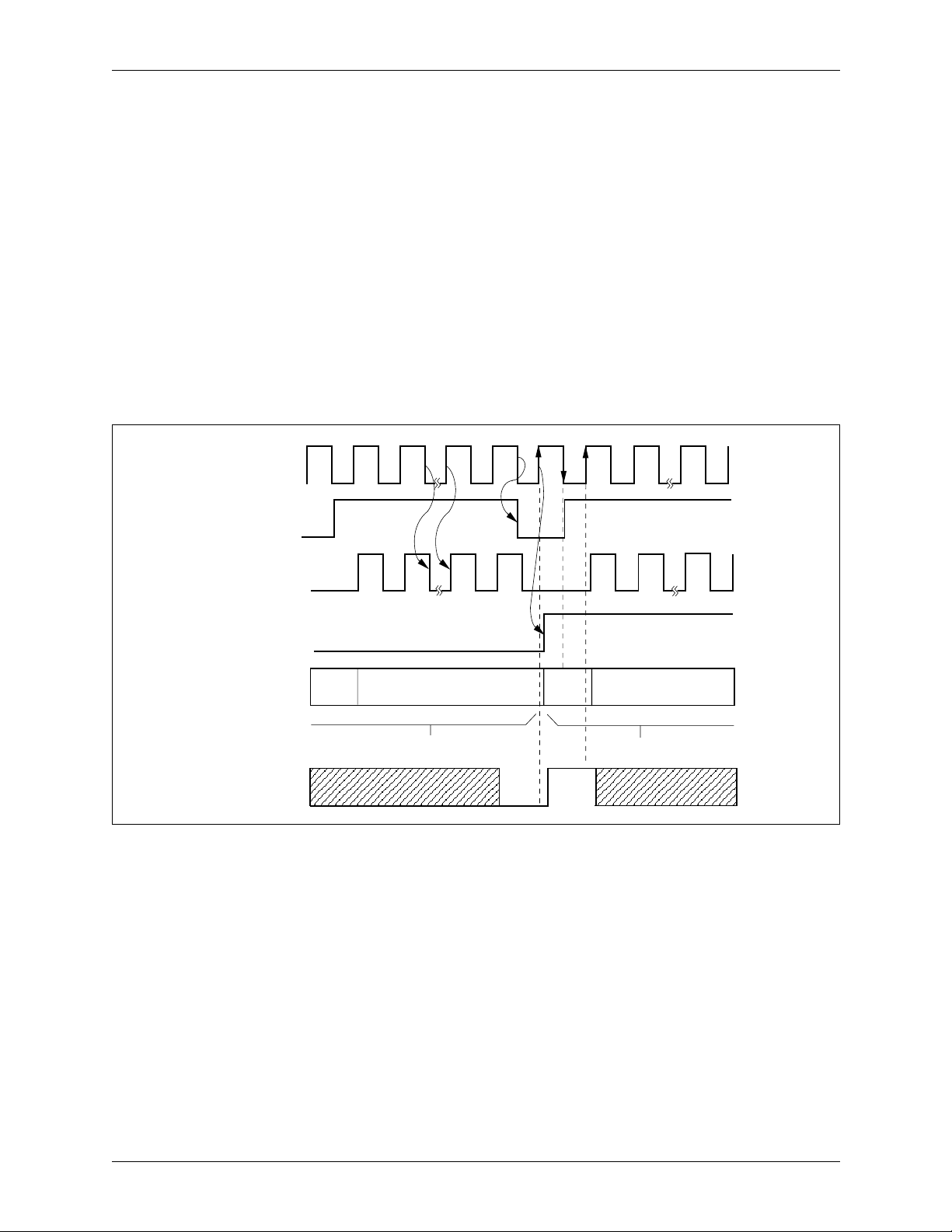
If the TDAT[7]/TXSYI M-frame sync signal is provided, it is sampled on the
rising edge of TXCKI an d should ha ve a l o w-to-h igh tran sition from t he last bit of
the M-frame (bit 680 of subframe 7) to the X1 bit (bit 1 of subframe 1). TXSYO
is clocked out by the rising edge of TXCKI and may be used for synchronization
of external circuitry. Serial data may alternatively be provided in response to the
TXBCK/TXGAPCK pin without the need for pro vidi ng frame synchroni zation or
ov erhea d bit sl ots. The gapped clock output is a gat ed v ersi on of T XCKI with one
pulse gapped for each overhead bit position (one pulse every 85 clock cycles). A
transmit overhead VALFCS/TXOVH bit position indicator pulse is available
when the PPDL is not selected. This pulse is clocked out on the falling edge of
TXCKI and may be of use for providing overhead bits exter nally. A timing
diagram is presented in Figure 2-4 with propagation delays shown as negligible.
Refer to the Electrical and Mechanical Specif ications chapter for actual
propagation delay specifications.
Figure 2-4. Transmitter Timing for Serial DS3 Mode
TXCKI
VALFCS/
TXOVH
TXBCK/
TXGAPCK
TXSYO
TDAT[6]/TXDATI
(Serial In)
TDAT[7]/TXSYI
(Sync In)
Low During Subframe 7
F4
84 Info Bits
Subframe 7
84 Info BitsX1
Subframe 1
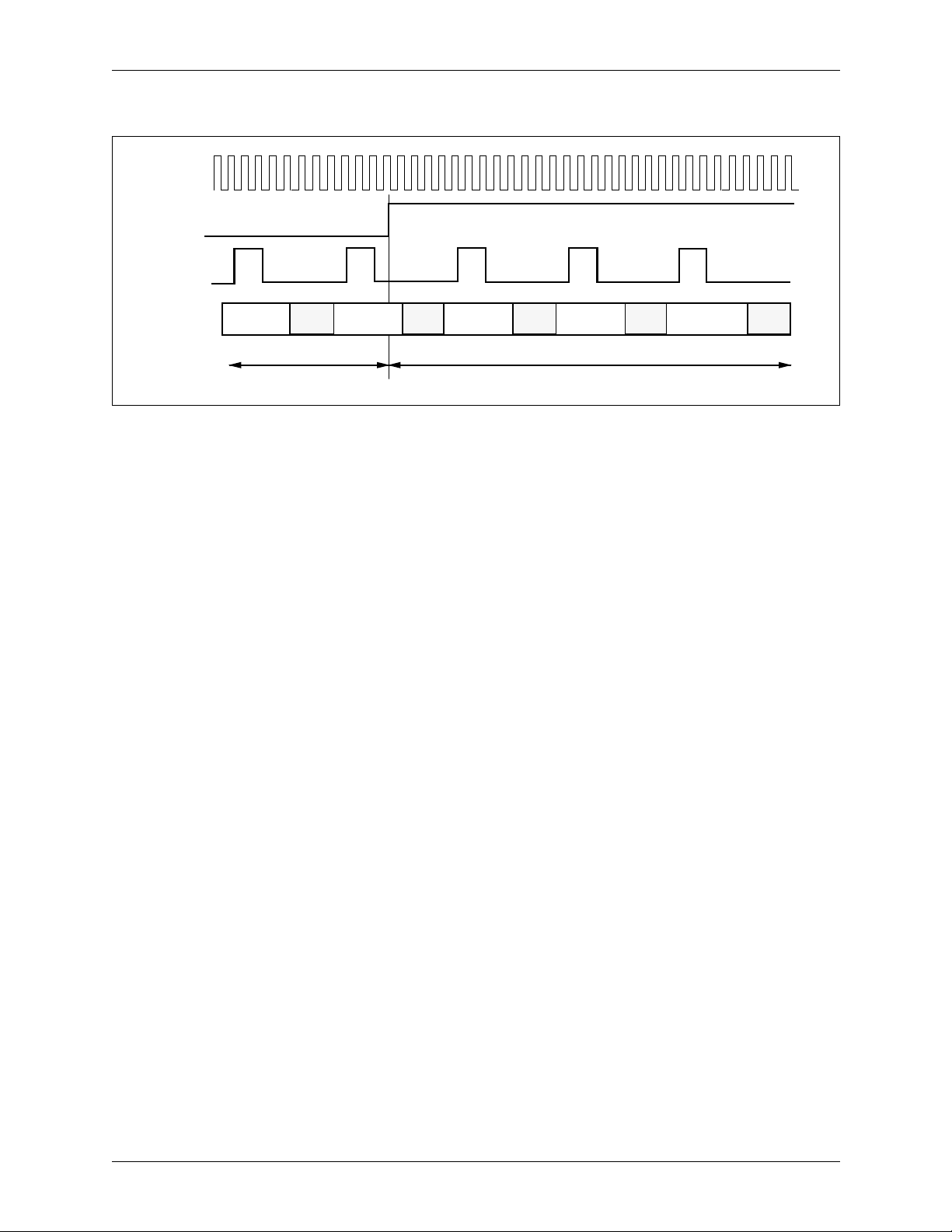
Figure 2-5 illustrates the transmitter timing for the parallel DS3 mode. This
mode is enabled by setting the Parallel Da ta Enable bit [ParaEn;CR04.3] in the
Feature Control Register and setting the Disable PPDL Transparency bit
[DisPPDL;CR05.1] in the PPDL Control Register [CR05;0x05]. The SNDMSG
pin should be tied high and the SNDFCS tied low to ensure that flags or FCS
bytes are not transmitted.
2-8 Conexant 100441E
Page 31
CN8330 2.0 Functional Description
DS3/E3 Framer with 52 Mbps HDLC Controller
Figure 2-5. Transmitter Timing for Parallel DS3 Mode
TXCKI
TXSYO
TXBCK/
TXGAPCK
TDAT[7:0]
Data
Subframe 7 Subframe 1
Data Data Data
2.3.3 E3 Mode
The clock and data edges for E3 mode have the same relationship as in DS3
mode. The synchronization overhead for E3 mode is 12 contiguous bits in each
frame rather than being distributed throughout the frame. The input bits are
synchronized to the M-frame sync signal, which can be externally provided or
internally generated f rom the M-fr ame sync sig nal. Seri al input data must contain
bit positions for the overhead bits, although these are not used unless external
insertion is enabled. The clock frequency is nominally 34.368 MHz and the
transmit data input is sampled on the falling edge of the clock signal. The path
delay of the transmitter from the serial data input to the positive and negative line
driver outputs is seven cycles of the transmit clock. This delay includes HDB3
encoding. The delay from the serial data input to the NRZ output is two clock
cycles and the coding delay of the HDB3 encoder is five clock cycles.
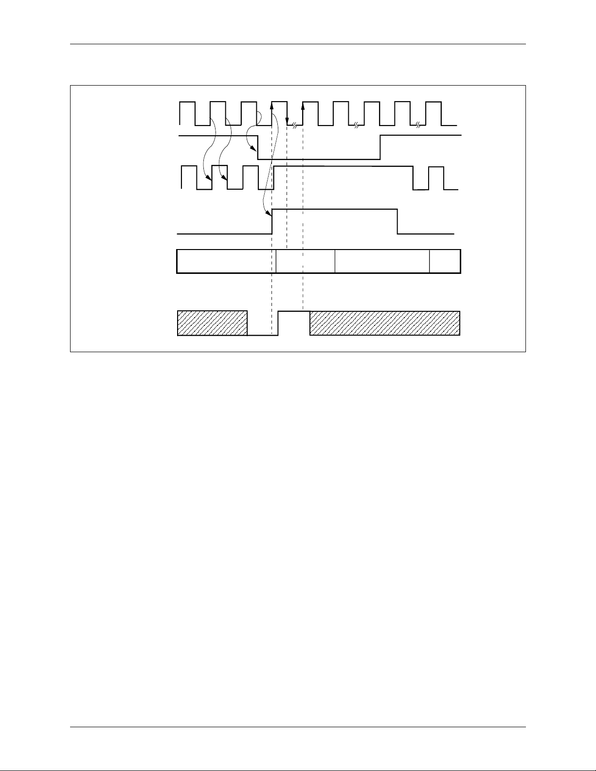
The TDAT[7]/TXSYI signal should have a low-to-high transition from the last
bit of the M-frame (bi t 1536) to the first bit of the FAS (bit 1). TXSYO may be
used to synchronize external circuitry. Serial data may be provided alternatively
in response to the TXBCK/TXGAPCK output without providing frame
synchronization or overhead bit slots. Figure 2-6 illustrates the timing with
propagation delays shown as negligible. Refer to the Electrical and Mechanical
Specifications chapter for actual propagation delay specifications. Note that in E3
mode gapped clock TXBCK/TXGAPCK is one clock cycle late relative to the
overhead bit positions when compared to the same relationship in DS 3 mode.
This clock can still be used for data input to the transm itter. The last data bit
clocked in ext ernal circuitry by the gapped clo ck output should be he ld during the
overhead interval and will be sampled by the first falling edge of TXCKI after the
overhead interval. This bit will appear as the first bit in the information field after
the overhead field.
2.3 Transmitter Operation
Data
100441E Conexant 2-9
Page 32
2.0 Functional Description CN8330
2.3 Transmitter Operation DS3/E3 Framer with 52 Mbps HDLC Controller
Figure 2-6. Transmitter Timing for Serial E3 Mode
TXCKI
VALFCS/
TXOVH
TXBCK/
TXGAPCK
TXSYO
Low for 12 Bits (FAS,A,N)
High for 12 Bits (FAS,A,N)
TDAT[6]/TXDATI
(Serial In)
TDAT[7]/TXSYI
(Sync In)
2.3.4 Framing Bit Generation
In DS3 mode, all F and M framing bits are automatically generated by the
transmitter circuitry. Additionally, the transmitter calculates the parity of each
M-frame and inserts this data into bits P1 and P2 of the following M-frame. Bits
X1 and X2 contain ones unless the Transmit Alarm Control 0 bit [TxAlm0;
CR00.4] in the Mode Control Register [CR00;0x00] is set. If set, bits X1 and X2
contain zeros. If C-bit parity mode is selected, all C-bit positions are generated
automatically by the transmitter if the External C-Bit Insert bit [ExtCBit;CR00.2]
is low. If high, all C-bits are generated internally except for the CP (subfram e 3)
an FEBE (subframe 4) bit positions. These bits must be provided on the CBITI
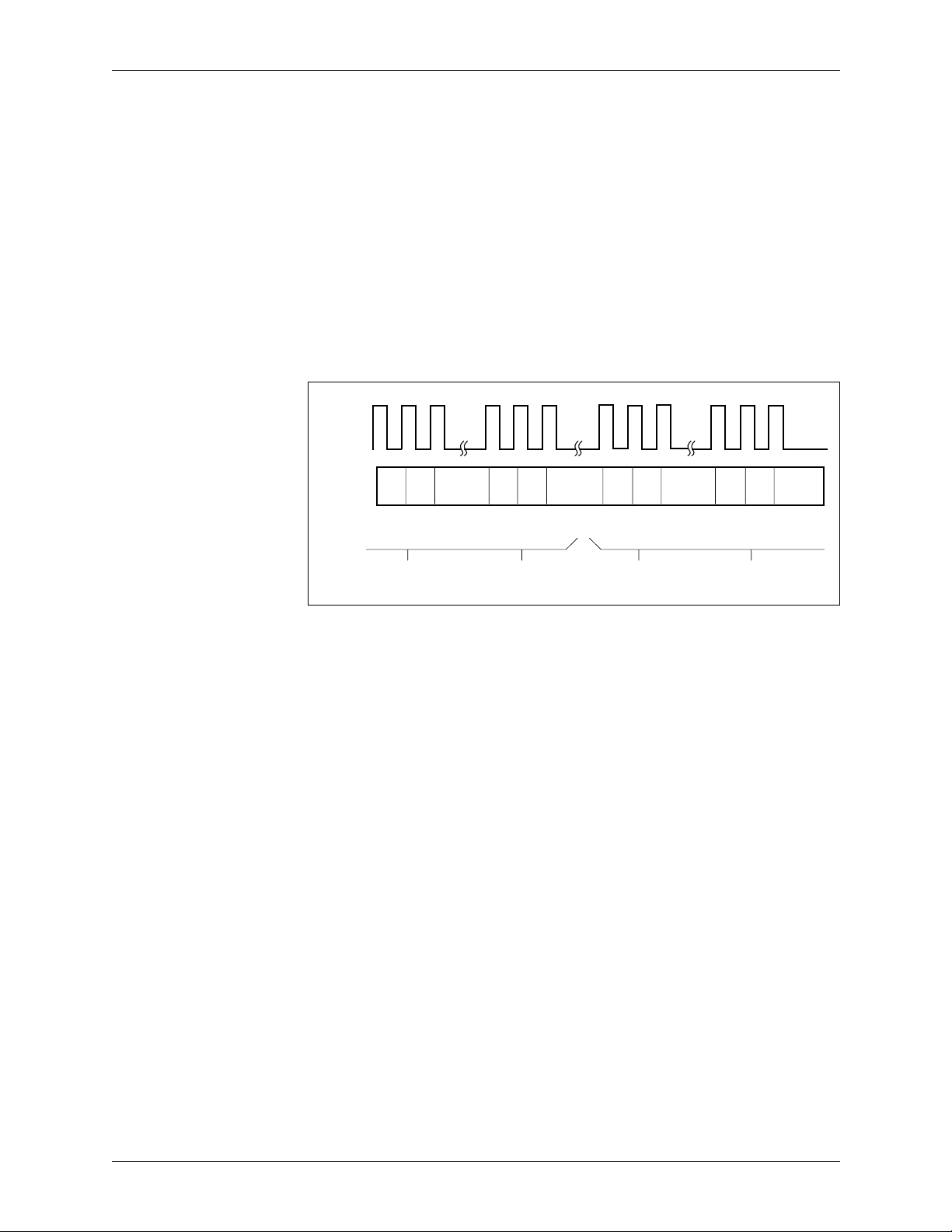
pin at the proper time in response to TXCCK as shown in Figure 2-7. The CBITI
data must be valid on the falling edge of TXCCK. This allows the chip to be used
in a repeater mode wit h pa ss-t hr ou gh o f t he p ath par i t y an d FE BE i nformation. If
C-bit parity mode is not selected, all C-bit positions come from either the serial
data stream or the CBITI pin depending on the ExtCBit setting in the Mode
Control Register. The X, P, M, and F bit positions may be inserted from the
transmit serial data stream by setting External Overhead Insert bit
[ExtOvh;CR00.3] high.
10-Bit FAS
A/N/11001520/1524 Info Bits
Info
2-10 Conexant 100441E
Page 33
CN8330 2.0 Functional Description
DS3/E3 Framer with 52 Mbps HDLC Controller
In E3 mode, the FAS pattern is auto matically generated by the transmitter
circuitry. The transmitter also inserts the A-bit as determined from the Transmit
Alarm Control 1 bit [TxAlm1;CR00.5 ] and the N-bit from the terminal data link
circuitry. If ExtCBit is high, the N-bit must be provided on the CBITI pin in
response to the rising edge of TXCCK. The TXOVH/VALFCS and TXSYO
signals are active during the 12 bits of overhead. If the PPDL is enabled, the
transmitter also inserts a 1100 pattern after the normal 12-bit framing sequence
for a total of 16 overhead bits. This 16-bit pattern is for conformance with draft
standard prETS 300 214 for SMDS applications. In this mode, the
VALFCS/TXOVH and TXSYO signals are active during all 16 bits of overhead.
All overhead bits can be inserted via the serial data input by setting the ExtOvh
bit high.
Figure 2-7. C-Bit Input Timing
TXCCK
CBITI
C1 C2 C3 C1 C2 C3 C1 C2 C3 C1 C2 C3
2.3 Transmitter Operation
2.3.5 Alarm Signal Generation
Three alarm signals, yellow, AIS, and idle, can be generated by the transmitter in
DS3 mode by setting the TxAlm[ 1,0] bit pair in the Mode Control Register.
The yellow alarm is contained in the X1 and X2 bits. The X1 and X2 bits are
normally set to 1. The yellow alarm (X1 and X2 bits = 0) can be sent by setting
the TxAlm bit pair to 01.
The AIS signal is enabled by setting the bit pair to 11. The AIS signal has
valid framing and parity, all C-bits set to zero regardless of framing mode, both
X-bits set to one, and the payload set to a 1010... pattern starting with 10 after
each overhead bit.
The idle code signal is enabled by setting the bit pair to 10. The idle code
signal has valid framing and parity, both X-bits set to one, and the pay load set to a
1100... pattern starting with 11 after each overhead bit. If the framing mode is
M13, all C-bits are set to z ero during transmission of the idle signal. If the
framing mode is C-bit parity, the C-bits in subframe 3 are set to zero, and the
other C-bits are from the selected source. This allo ws full use of the terminal data
link and transmit FEAC channel during transmission of idle code.
Subframe 1Subframe 7
Subframe 2Subframe 6
100441E Conexant 2-11
Page 34

2.0 Functional Description CN8330
2.3 Transmitter Operation DS3/E3 Framer with 52 Mbps HDLC Controller
In C-bit parity mode with inte rnal sourcing of th e C-bits, FEBE alarms are
generated automaticall y in the transmi tter whe n the recei ve r detects eit her a frame
bit error or a C-bit parity error in an M-frame. The 3-bit FEBE pattern that is
transmitted is contained in the FEBE Pattern Bit Field [FEBEC[3:1];CR04.2:0] of
the Feature Control Register. Bit 2 is placed in the C1 position of subframe 4
during the alarm condition, bit 1 is placed in the C2 position, and bit 0 is plac ed in
the C3 position. When no alarm condition is present, the FEBE channel contains
all ones. Therefore, to prevent disabling proper FEBE operation, the FEBE field
should be written to any combination other tha n 111.
An unframed, all-ones signal can be transmitted by setting both TxAlm0 and
TxAlm1 to a 1 and ExtOvh cleared to a 0.
In E3 mode, the AIS (unframed all-ones) is enabled by setting TxAlm0 high.
The yellow alarm is enabled by setting TxAlm1 high. This causes the transmitted
A-bit to be set to a one.
2.3.6 Terminal Data Link Transmitter
The terminal data link transmitter consists of the three C-bits in subframe 5 of the
M-frame in DS3 mode or the N-bit in E3 mode and uses the LAPD protoc o l.
When the Send Message bit [TxMsg;CR01.0] of the Terminal Data Link Control
Register [CR01;0x01] is lo w, the data link transmitter is con tinuousl y sending idle
flags (01111110). When high, message transmission is initiated. Transmission of
the FCS bytes is controlled by the Send Frame Check Sequence bit
[TxFCS;CR01.1]. If a nonstandard FCS is required, it may be loaded into the
message buffer and transmitted as part of the message. A message in progress
may be abandoned b y setting the Abort Message bit [TxAbort;CR01.2]. T his will
cause an abort flag (11111110) to be transmitted, followed by idle flags, until the
Send Message bit is reactiv at ed. Two consec utiv e messages ma y share endi ng and
beginning idle flags. The transmitter can be disabled by setting the Disable
Terminal Data Link Transmission bit [DisTxTDL;CR01.6] to a one. This causes
all ones to be sent in the data link bit positions.
The terminal data link transmitter is under control of the C-Bit Parity
Mode/Enable DLINT/SOURCELB (CBitP/DL;CR00.0), E3 Framing Mode
[E3Frm;CR00.1], External C-Bit Insert, and Transmit Alarm Control bits in the
Mode Control Register. In the Terminal Data Link Control Register, the
transmitter is under the control of the TxMsg, TxFC S, TxAbort, Send Byte
[TxByte[2:0];CR01.5:3], and DisTxTDL bits. An interrupt for use with data link
operations is available on the DLINT/SOURCELB output pin and status bits for
determinin g the interrupt source are located in the Data Link Interrupt Status
Register [SR02;0x12].
The framer mode must be set to either C-bit parity mode or E3 mode for
terminal data link transmission to take place. In C-bit parity mode, the three
C-bits in subframe 5 of the M-frame will be used for transmission. In E3 mode,
the N-bit will be used for transmission. When E3 mode is selected, the CBitP/DL
bit must also be set to enable interrupts on the DLINT/SOURCELB pin. If neither
mode is set, terminal data link transmission will not take pl ace. If the ExtC Bit bi t
is set in E3 mode, terminal data link transmission will be disabled. In C-bit parity
mode, ExtCBit has no effect on te rminal data link transmission. Setting the
Transmit Alarm Control [1,0] bits for transmission of AIS or all ones in either
C-bit parity mode or E3 mode will disable transmission of the terminal data link.
Transmission of yellow alarms or idle codes has no effect on terminal data link
transmission.
2-12 Conexant 100441E
Page 35

CN8330 2.0 Functional Description
DS3/E3 Framer with 52 Mbps HDLC Controller
If the framer is in a mode that allows data link transmission as described
previously, then the Terminal Data Link Control Register is the main control
register used for t ransmit dat a link o perati ons. The DisTxTDL bi t must be set low
to enable operation of the data link. If high, an all-ones signal will be transmitted
in the data link bit positions in the outgoing seria l stream. With the data link
enabled, the TxMsg, TxFCS, and TxAbort bits control operation. The
TxByte[2:0] bits form a pointer to the Transmit Terminal Data Link Message
Buffer [TxTdl;0x30–0x37] used by the data link transmitter.
The transmitter implements an LAPD data link per CCITT standard Q.921.
The functions pro vided b y the data link t ransmitter circuitry are transparenc y zero
stuffing, FCS generation, idle flag generation , and abort flag generation. The total
length of the message has no restrictions. Q.921 requires all messages be integral
numbers of 8-bit bytes. The transmitter can only transmit 8-bit bytes. Byte
transmission time for the transmitter is approximately 284 microseconds in C-bit
parity mode and approximately 357 microseconds in E3 mode.
The Transmit Terminal Data Link Message Buf fer is an 8 -byt e buffe r pro vided
for the transmit data link channel to minimize processor interruptions. Filling of
this buffer is accomplished by the processor in the same manner as writes to
control registers. This buffer can be read as well as written to verify co ntents. The
buffer is divided into two halves to reduce the real-time requirements on the
processor. The processor loads four bytes at a time, while the data link transmitter
reads from the other half of the buffer. This gives the processor at least 1 msec to
assemble the next four b ytes of message for transmi ssion before the ne xt in terrupt
is issued. Interrupts are issued each time the transmitter circuitry reaches a 4-b yte
buffer boundary.
The transmitter must initialized with bits 0 through 6 of the Terminal Data
Link Control Register written to zero. This will enable the transmitter to send idle
flags on the data link. No interrupts are generated when the data link is sending
idle flags, thus no processor intervention is required until a message is to be sent.
2.3 Transmitter Operation
2.3.6.1 Sending a Message
Beginning with an idle channel, th e processor writes the first four bytes of
message data to the Transmit Terminal Data Li nk Message Buffer. The first byte
of data to be transmitted should be written to address 0x30. The message is read
from the buffer in ascending order starting at address 0x30 and ending at address
0x37. The Least Significant Bit (LSB) in each byte is the first transmitted. This
buffer may be written well before the message is to be sent, if desired. After the
first block of data is present in the buffer memory, the processor writes to the
Terminal Data Link Control Register to begin transmission (TxMsg = 1,
TxByte[2:0] = 011, TxFCS = 0, TxAbort = 0). The 3-bit TxByte[2:0] field is
functionally split into two parts. The Most Significant Bit (MSB) indicates to the
transmitter circuitry which half of the buffer to read f rom next. The two LSBs
indicate the stop location, i.e., where the last message byte is located. When the
new controls are latched by the transmitter circu itry, the processor will be
interrupted for the next set of controls. Now, the processor has up to 1 msec to
write a new set of controls to the control register. The processor may now also
write the next block of data to the next half of the message buffer.
When the end of a message is reache d , or in the e v ent of a short message, there
may not be exactly 4 bytes remaining. In this case, the processor writes the
remaining data to the message buffer as usual. The processor now must write the
highest location used to the TxByte[2:0] field. Also, the TxFCS bit is set to 1.
This causes the FCS to be sen t a fter this last block of data.
100441E Conexant 2-13
Page 36

2.0 Functional Description CN8330
2.3 Transmitter Operation DS3/E3 Framer with 52 Mbps HDLC Controller
When this set of controls is latched, the processor will be interrupte d. At this
time, a new message ma y be sent, or the TxMsg bit ma y be set to zero to send id le
flags. If a new message is to be sent immediately, the next half of the transmit
buffer can be written, and the Terminal Data Link Control Register optioned
accordingly. This will result in only one idle flag being transmitted b et ween
messages. If there is no new message ready, the processor must write TxMsg to
zero. If this is not done within 1 msec, undefined data will be transmitted.
2.3.6.2 Aborting a Message
2.3.6.3 Transmitter Interrupts
To abort a message in progress, the control ler writes th e TxAb ort bit to one in the
Terminal Data Link Control Register. The transmitter will finish sending the
message byte in progress, then transmit an abort flag (11111110). After writing
the abort signal to the control register, a second write may follow immediately to
cause the transmitter to go to the idle condition, or to transm it another message.
In the latter case, the abort flag will be follo w ed b y one id le flag, and then the new
message will begin. If the second write is not performed, the formatter will
continue to transmit abort flags until instructed otherwise.
The transmitter genera te s an interrupt when it has latched the present set of
controls and is ready for a new set. There will not be any interrupts during the
transmission of idle flags. Therefore, to start a message from an idle condition,
the first half of the buffer and the proper control bits are written by the processor.
When the circuit latc hes these controls internally, an interr upt will immediately
be issued for the next set of control bits. The processor then has up to 1 msec (4
byte periods) to respond to the interrupt. The Data Link Interrupt Status Register
[SR02;0x12] indicates the sourc e of the interrupt but not the cause. The controller
software must know from message context what response is required. The
interrupt is an active low level, not a pulse. The in terrupt will be cleare d up on th e
writing of the Terminal Data Link Control Register. A write operation must be
performed to clear the cur r ent interrupt and prevent missing later interrupts.
If the interrupt is a mid-message interrupt, a new data link control word must
be written, with b ytes equ al to the endi ng lo catio n of t he ne xt message b lock. T he
MSB of TxByte[2:0] will inform the transmit circuitry which half of the buffer to
read next.
Interrupts from the Terminal Data Link Transmitter will appear in the
Transmit Terminal Data Link Interrupt bit [TxTDLI tr;SR02.3]. Int errupts must be
enabled to appear on DLINT/SOURCELB by setting the CBitP/DL b it to a 1 in
the Mode Control Regi ster in either C-bit parity or E3 mode.
2-14 Conexant 100441E
Page 37

CN8330 2.0 Functional Description
DS3/E3 Framer with 52 Mbps HDLC Controller
2.3.6.4 Transmitter Control Example
This example will show the sequence necessary to transmit a 10-byte hex
message starting in the low half of the transmit buffer. With the transmitter in the
idle state, the processor would execute the following sequence:
write byte 1 to address 0x30
write byte 2 to address 0x31
write byte 3 to address 0x32
write byte 4 to address 0x33
write 0x19 to address 0x01 (TxByte[2:0] = 011, TxMsg = 1)
at TX Interrupt:
write byte 5 to address 0x34
write byte 6 to address 0x35
write byte 7 to address 0x36
write byte 8 to address 0x37
write 0x39 to address 0x01 (TxByte[2:0] = 111, TxMsg = 1)
at TX Interrupt:
write byte 9 to address 0x30
write byte 10 to address 0x31
write 0x0B to address 0x01 (TxByte[2:0] = 001, TxMsg = 1, TxFCS = 1)
at TX Interrupt:
write 00 to address 0x01 (TxMsg = 0, TxFCS = 0)
2.3 Transmitter Operation
2.3.7 TxFEAC Channel Transmission
The third C-bit in subframe 1 of the M-frame is the Transmit Far End Alarm and
Control (TxFEAC) Channel. This channel uses a bit-oriented protocol and is
under control of the Transmit FEAC Channel Byte Register [CR03;0x03].
The TxFEAC Channel Transmitter is under control of the CBitP/DL, E3Frm,
and TxAlm[1,0] bits in the Mode Control Register and the Transmit FEAC
Channel Message Byte [TxFEAC[7:0];CR03.7:0] in the Transmi t FEAC Channel
Byte Register. An interrupt for use with TxFEAC channel operations is available
on the DLINT/SOURCELB output pin and status bits for determining the
interrupt source are located in the Data Link Interrupt Status Register.
The framer mode must be set to C-bit parity mode for TxFEAC channel
transmission to take pla ce. In C-bit parity mode, the last C-bit in subframe 1 of
the M-frame will be used for transmission. There is no TxFEAC channel
transmission in either E3 m ode or with the CBitP/DL bit set to zero. Setting
ExtCBit in C-bit parity mode has no effect on TxFEAC channel transmission.
Setting the TxAlm[1, 0] bits for transmission of AIS or all ones in C-bit parity
mode will disable transmission of the TxFEAC channel. Transmission of yellow
alarm or idle code in C-bit parity mode has no effect on TxFEAC channel
transmission.
100441E Conexant 2-15
Page 38

2.0 Functional Description CN8330
2.3 Transmitter Operation DS3/E3 Framer with 52 Mbps HDLC Controller
The Transmit FEA C Channel Byte Re gister controls the b yte to be transmitted
on the TxFEAC channel. All messages for transmission on this channel must be
in the form “0xxxmmm011111111". The rightmost bit of this sequen ce is the first
bit transmitted on the c hannel. To initiate transmission of a me ssage byte in the
TxFEAC channel, the desired byte in the form 0mmmxxx0 is written into the
Transmit FEAC Channel Byte Register. Transmission of the flag (11111111) is
automatic. Each time the message is sent, an interrupt will be issued on the
DLINT/SOURCELB pin and will appear in the Data Link Interrupt Status
Register to request a new byte from the processor. The Transmit FEAC Channel
Byte Register must be written to clea r the interrupt. If multiple transmis sions of
the same byte are desired, the processor should rewrite the desired byte on each
interrupt and count the interrupts until the desired number of transmissions have
taken place. Interrupts from the TxFEAC channel will occur at a rate of
approximately one interrupt per 1.7 msec.
Transmit FEAC clears the internal data shift buffer after sending CR03
contents unless the host has again written to CR03. When the host writes CR03,
CN8330 transfers CR03 contents to an internal data shift buffer and then
immediately raises an interrupt (SR02.1) which tells the host that another
codeword (or the same one) can be written. After the interrupt the host must write
to CR03 within 1.7ms to keep sending codewords, else after sending the shift
buffer contents C N8330 will automat icall y return to sending id le (all ones) FEA C
codewords.
In summary, Transmit FEA C clears the internal data shift buffer after sending
the transmit FEAC channel byte from the CR03 register contents unless the host
has again written to this register (CR03). When the host writes to Transmit FEAC
Channel byte Register (CR03), CN8330 transfers the contents to an inte rnal data
shift buffer and then immediately raises a n interru pt in the Data Link Interrupt
Status Register (SR02.1) which tells the ho st that an ot her cod e word (or the same
one) can be written. After the interrupt, the host must write to Transmit FEAC
Channel Byte Register (CR03) wit hin 1.7 ms t o k ee p sendi ng code words, or else
after sending the shift buffer contents CN8330 will automatically return to
sending idle (all ones) FEAC codewords.
If a one is in either the MSB or LSB position of the TxFEAC field, then
continuous transmission of idle flags is enabled and no interrupts wi ll be issued
until a byte of the proper format is written to the Transmit FEAC Channel Byte
Register.
Interrupts from the TxFEAC channel transmi tte r will appear on Transmit
FEAC Channel Interrupt bit. Interrupts must be enabled to appear on
DLINT/SOURCELB by setting the CBitP/DL bit in the Mode Control Register.
2.3.8 PPDL Transmitter
The payload portion of the CN83 30 data strea m can come fro m an internal PPDL
formatter that provides an e xternal byte-wide da ta interface and a by te clock. This
source is enabled by setting the ParaEn bit in the Feature Control Register. The
PPDL formatter is controlled by signals applied on the SNDMSG and SNDFCS
pins. Both byte-wide and nibble-wide inputs can be provided. Optional HDLC
formatting with 16-bit or 32-bit FCSs is provided.
2-16 Conexant 100441E
Page 39

CN8330 2.0 Functional Description
DS3/E3 Framer with 52 Mbps HDLC Controller
HDLC mode is selected by setting the ParaE n bit of the Feature Control
Register high and the DisPPDL bit of the PPDL Control Register low. Operation
is controlled by the SNDMSG and S NDFCS pins. If no message is in progre ss,
idle flags (01111110) are continuously transmitted in the data payload. Setting
SNDMSG high initiates message transmission. Data bytes and control signals are
provided in response to the rising edge of the TXBCK/TXGAPCK pin and are
sampled internally after th e falling ed ge. T he data and control s should be he ld for
a full period. The LSB of t he transmitted bytes is applied to TDAT[0] and the
MSB to TDAT[7]; transmission is LSB first. The transmitter performs automatic
zero stuffing for transparency and FCS calculation for the data. The message
must be an integral number of bytes in length. The FCS is 16 or 32 bits in length
depending on the setting of the 32-bit CRC Select bit [CRC32;CR05.2] in the
PPDL Control Register. If this bit is low, a 16-bit FCS is calculated with the
polynomial:
If the CRC32 bit is high, a 32-bit FCS is calcu lated. SNDFCS must be high
for four cycles of the transmit byte clock and the FCS is calculated with the
polynomial:
32+x26+x23+x22+x16+x12+x11+x10+x8+x7 +x5+x4+x2
x
The FCS is transmitted by setting both the SNDMSG and SN DFCS pins high
after the last data byte has been transm itted. An abort sequence may be
transmitted by setting SNDFCS high while SNDMSG is set low. Timing for the
transmit operation is shown in Figure 2-8.
16+x12+x5
x
2.3 Transmitter Operation
+1
+x+1
Figure 2-8. PPDL Transmitter Timing
TXCKI
TXBCK/TXGAPCK
TDAT[7:0]
SNDMSG
SNDFCS
Data
Data
100441E Conexant 2-17
Page 40

2.0 Functional Description CN8330
2.3 Transmitter Operation DS3/E3 Framer with 52 Mbps HDLC Controller
TXBCK/TXGAPCK is generated from TXCKI and has a duty cycle of 25
percent. TXBCK will nominall y be one-eight h the TXCKI fre quency but is
influenced by HDLC tra nsparenc y bit insertions and DS3/E3 o verhe ad bits. In the
absence of any transparency bit insertions or overhead bits, there will be one
pulse on TXBCK for every eight clock cycles of the TXCKI input. When a
transparency bit is inserted into th e serial transmit data stream, the TXBCK
period will be lengthened to nine clock cycles of TXCKI (or up to 11 cycles if
two transparency bit insertions and a DS3 overhead bit land in the same data octet
interval). TXBCK/TXGAPCK is present continuously even during the
transmission of idle flags. The actual setup times on TDAT[7:0], SNDMSG, and
SNDFCS relative to the rising edge of TXBCK ar e negative. Therefore, it is
possible to read data and contr ol from a RAM or FIFO buffe r with the rising ed ge.
The CN8330 will sample the data after the falling edge. This allows FIFOs or
RAMs with access times of 35–40 nsec to be used.
The parallel interface can be used without tra nsparency bit insertion by se tting
the DisPPDL bit in the PPDL Control Register to a 1. In this mod e , SNDMSG is
held high and SNDFCS is held low so that no flags or FCS bytes are transmitted.
Byte synchronization in the transmitter and re ceiver is achieved from the
M-frame sync alignment. This allows the byte-wide interface to be used as the
data input for non-HDLC payloads rather than the serial input pin. Data is
inserted on the TDAT[7: 0] pins in response to TXBCK/TXGAPCK just as in the
HDLC mode. Data bytes are transmitted LS B first. If E3 m ode is enabled, the
transmitted bytes are byte aligned after the 16 overhead bits for a total of 190
bytes per frame. To accommodate E3 SMDS applications, the input bytes should
be applied to the TDAT[7:0] pins in reverse bit order so that the MSB will be
transmitted first.
2-18 Conexant 100441E
Page 41
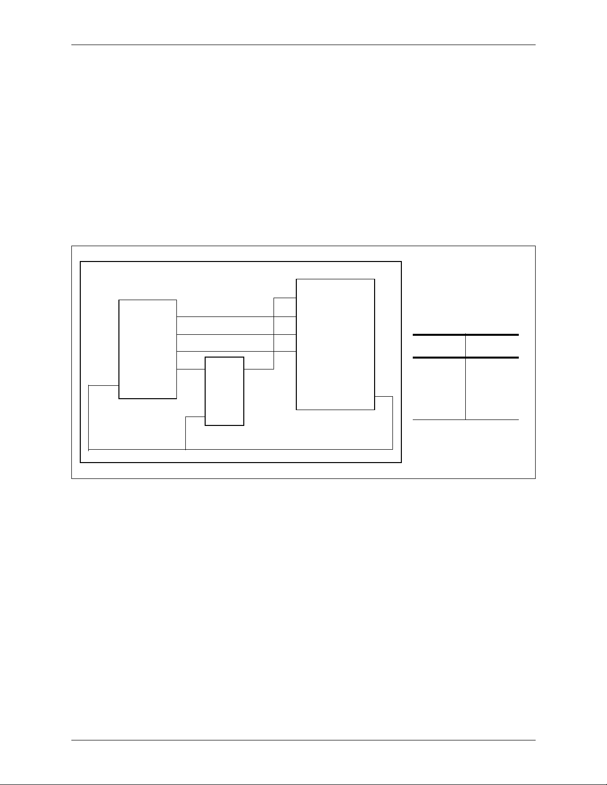
CN8330 2.0 Functional Description
DS3/E3 Framer with 52 Mbps HDLC Controller
The PPDL transmitter can be used with a nibble-wide interface for DS3
SMDS applications if desired. To enable nibble-wide transmission, both the
Nibble Mode Enable [Nibble;CR05.0] and DisPP D L bits in the PPDL Control
Register should be set to one. Data should be inserted on the TDAT[3:0] pins;
MSB on TDAT[2], second MSB on TDAT[1], next MSB on TDAT[0], LSB on
TDAT[3] in response to T XBCK/T XGAPCK (which now occurs ev e ry 4 bits) . I n
nibble mode, the nibbles are transmitted MSB first and are nibble-aligned after
each overhead bit in the DS3 frame for a total of 21 nibbles per 85-bit data block.
Nibble mode should not be used for E3 applications. In this mode (Nibble mode
and PPDLONLY pin = 0), the transmit PPDL interface shifts the serial data by
one bit. This anomaly (only on the transmit side) can be remedied by the circuit
shown in Figure 2-9.
Figure 2-9. Nibble Mode with the PPDLONLY Control Pin Low
Nibble Data
Register
Q3
Q2
Q1
Q0
CK
DQ
CK
TDAT[3]
TDAT[2]
TDAT[1]
TDAT[0]
CN8330
TXBCK
2.3 Transmitter Operation
Data Bit Input Pin
MSB
2SB
1SB
LSB
Q Output
TDAT[2]
TDAT[1]
TDAT[0]
D Input
TDAT[3]
•
D-Type FF
100441E Conexant 2-19
Page 42
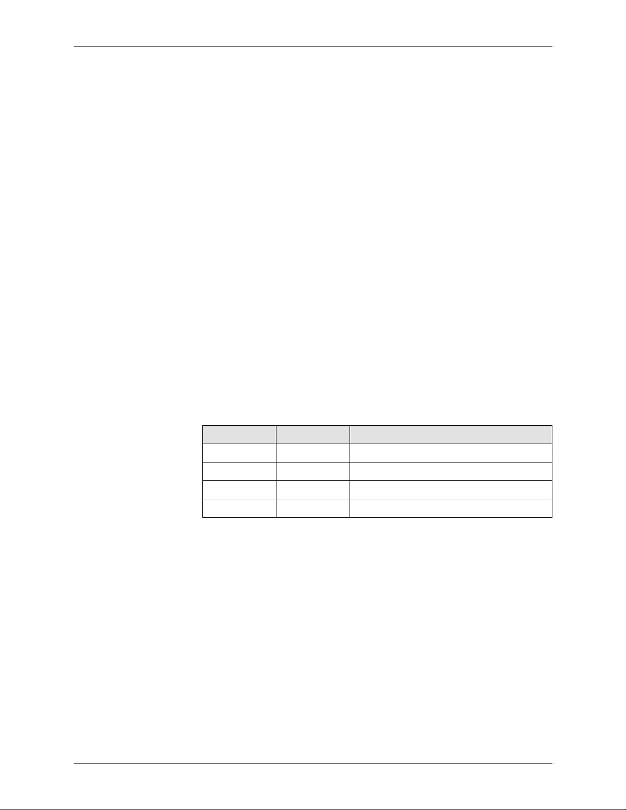
2.0 Functional Description CN8330
2.3 Transmitter Operation DS3/E3 Framer with 52 Mbps HDLC Controller
FCS calculation can be limited to the first N bytes of the transmitted message
by setting the Limit Frame Check Se quence Calculation [LimitFCS;CR05.3]
control bit. In this mode, the FCS is calculated on t he first N bytes transmitted
after the opening flag and then held until the e nd of the message. It is then
appended to the end of the messag e in normal fashion. T he desired number N can
be from 1 to 16 (a value of 0 gives N=16) and is loaded in the Frame Check
Sequence Calculation Count [FCSCnt[3:0];CR05.7:4] control field. This allows
FCS calculation only on the header information in a T1 packet voice format.
2.3.9 PPDLONLY Mode
The transmitter can be placed in a mode where the entire transmit st ream consi st s
of data with no DS3/E3 overhead bits inserted. This mode is enabled b y providing
a high input on the PPDLONLY input pin. This mode allows the CN8330 to be
used as a high-speed PPDL formatter and can be used at any clock rate up to the
full 52 MHz capability of the device. Data and controls are provided to the
transmitter in response to the transmit b yte cl ock. When PPDLONLY mode is set,
the transmit NRZ data stream is available on the RXCCK/TXNRZ pin.
2.3.10 Transmitter Outputs
The TXPOS and TXNEG pins provide a variety of signals depending on the
control bits in the Feature Control Register. Table 2-1 summarizes the available
output combinations when the Test Equipment Feature Select bit
[TstEqSel;CR04.7] is low.
Table 2-1. Transmit Encoding Options
DisEnc AMI/LCV2 Transmit Output
0 0 B3ZS/HDB3 Encoded Data on TXPOS, TXNEG
0 1 AMI Encoded Data on TXPOS, TXNEG
1 0 NRZ Data on TXPOS, Transmit Clock on TXNEG
1 1 NRZ Data on TXPOS, Transmit Clock on TXNEG
2-20 Conexant 100441E
Page 43

CN8330 2.0 Functional Description
DS3/E3 Framer with 52 Mbps HDLC Controller
2.3.11 Test Equipment Specific Features
Additional features in the transmitter are available if parallel mode is not selected
(ParaEn = 0). The RDAT[7]/TXNRZ pin becomes an output of the transmit data
in NRZ format before being presented to the B3ZS/HDB3 encoder. The
TDAT[5]/TXENCI p in is an input di rectl y to the B3Z S/HDB3 encod er . This in put
is selected if the TstEqSel bit is set high. This al lo ws either d irect insertion of data
for B3ZS/HDB3 encoding or modification of the transmit data via RDAT[7] and
reinsertion of this stream for encoding. The TDAT[4]/LCVERRI pin is an input
that allows insertion of line code violations into the transmit data stream. This
input is also enabled w he n the TstEqSel bit is set high. Wh en enab led, a line code
violation will be inserted at the next opportunity each time the LCVERRI pin is
high. The input should be high for onl y one cloc k cycle to gu arantee that onl y one
line code violation is generated. If the AMI/LCV2 control bit in the Feature
Control Registe r is low, a v al id i nsertion opportunit y is defined as the second 1 in
a 11 sequence. If AMI/LCV2 is high, a valid insertion opportunity is defined as
the next B3ZS/HDB3 substitution. The opposite polarity of substitution pattern
will be inserted if an error is to be generated (a B0V/B00V instead of an
00V/000V or vice versa). This avoids the possibility of incorrectly emulating a
B3ZS/HDB3 substitution pattern and causing bit errors.
NOTE: B = Legal Bipolar Pulse; V = Bipolar Violation Pulse.
2.3 Transmitter Operation
100441E Conexant 2-21
Page 44

2.0 Functional Description CN8330
2.4 Receiver Operation DS3/E3 Framer with 52 Mbps HDLC Controller
2.4 Receiver Operation
2.4.1 Bipolar-to-Unipolar Conversion
The bipolar-to-unipolar recovery circuit includes the B3ZS/HDB3 decoding
circuit. Decoding is done according to TR-TSY-000009 for B3ZS or G.703 for
HDB3. A circuit detects the B3ZS/HDB3 signature and the substitution back to
three or four zeros is made. Substitution to three or four zeros is made on every
occurrence of 00V/B0V (B3ZS) or 000V/B00V (HDB3). Bipolar and line code
violations (other than those associated with a valid B3ZS/HDB3 signature) are
counted in the 16-bit DS3/E3 LCV Counter [SR12,SR13;0x25,0x26] that is
cleared when read. In DS3 mode, a substitution pattern of improper polarity (B0V
for 00V or vice versa) will be decoded to three zeros but will be counted as a
bipolar violation. Occurrences of three or more zeros before B3ZS decoding will
also be counted as a bipolar violation.
In E3 mode, Line Code Violations (LCVs) are counted in the DS3/E3 LCV
Counter. An LCV is defined by ITU-T O.161 as two consecutive BPVs of the
same polarity. Occurrences of four or more zeros before HDB3 decoding will not
be counted as an LCV.
B3ZS/HDB3 decoding can be defeated by connecting the RXPOS and
RXNEG inputs together and supplying NRZ input data to both pins or by setting
the AMI/LCV2 control bit high and supplying a non-encoded AMI signal on
RXPOS and RXNEG.
2.4.2 Receive FIFO
The receiver circuit contains a 16-bit FIFO buffer immediately following the
B3ZS decoding circuit to provide jitter elasticity of up to ± 5 unit intervals. The
data is clocked into the FIFO buffer with the incoming DS3CKI clock. Data is
clocked out of the FIFO buffer and into the remaining receiver circuitry by the
RXCKI which is a dejittered version of DS3CKI. The FIFO buffer circuit
provides a VCO control signal to indicate the phase relationship of the FIFO
buffer input and output clocks. Both clocks are divided by 16 internally to derive
the VCO output as shown in Figure 2-10. This signal can be used to control the
clock reco very circuit produ cing the smoothed RXCKI. The FIFO buf fer circuit is
bypassed and all receiver circuitry is clocked with DS3CKI if FIFEN is low.
RXCKI should be tied to ground if the FIFO buffer is disabled.
Figure 2-10. VCO Output Signal Timing
DS3CKI
÷ 16
RXCKI
÷ 16
VCO
Output
2-22 Conexant 100441E
Page 45
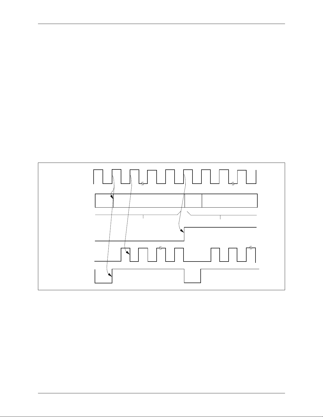
CN8330 2.0 Functional Description
DS3/E3 Framer with 52 Mbps HDLC Controller
2.4.3 Received Signal Output
The received unipolar signal is recovered and provided with a clock on RXDAT
and RXCLK. An M-frame synchronization signal and gapped clock are also
provided. Figure 2-11 shows a timing diagram for DS3 mode with negligible
propagation dela ys for the DS3 recei v er output signals. Refer to the Electri cal and
Mechanical Specifications section for actual propagation delay specifications.
RXMSY is low during subframe 7 preceding the X1 bit in the first subframe.
Outputs change on the rising edge of the receive clock except for the gapped
clock on RXBCK/RXGAPCK. This clock is an inverted version of RXCLK with
a gapped pulse every 85 bits. The receive clock will be nominally 44.736 MHz.
Data on RXDAT can be clocked into the user's circuit with the rising edge of the
RXBCK/RXGAPCK if it is desired to observe only data bits (there is no rising
edge present during the overhead bit positions). The rising edge of RXBCK will
be mid-bit for each payload bit in the serial stream. An overhead indicator
RDAT[6]/RXOVH is available when the PPDL is not enabled. This signal is low
for each bit position that is an overhead bit in the receive serial stream.
Figure 2-11. Recei ver Timing for Serial DS3 Mode
RXCLK
2.4 Receiver Operation
RXDAT
RXMSY
RXBCK/
RXGAPCK
RDAT[6]/
RXOVH
F4
84 Info Bits
Subframe 7
84 Info BitsX1
Subframe 1
100441E Conexant 2-23
Page 46

2.0 Functional Description CN8330
2.4 Receiver Operation DS3/E3 Framer with 52 Mbps HDLC Controller
Figure 2-12 illustrates the receiver timing for the parallel DS3 mode. This
mode is enabled by setting the ParaEn bit in the Feature Control Register and
setting the DisPPDL bit in the PPDL Control Register. The receive data is valid
on either the rising or falling edge of RXBCK.
Figure 2-12. Recei ver Timing for Parallel DS3 Mode
RXCLK
RXMSY
RXBCK/
RXGAPCK
RDAT[7:0]
data
Subframe 7 Subframe 1
Figure 2-13 illustrates a timing diagram for the E3 recei v e r output signal with
the PPDL enabled. The clock and data edge relationships are similar to those in
DS3 mode. The M-frame synchronization signal RXMSY is high during the
12-bit block corresponding to the 10-bi t FAS and the A and N bits. I f the P PDL is
enabled, the M-frame synchronization signal will be high for four additional bit
periods corresponding to the 1100 pattern found in SMDS formatted signals.
RDAT[6]/RXOVH will be low for 12 bits in serial mode and for 16 bits if the
PPDL is enabled.
Figure 2-13. E3 Receiver Output Timing
RXCLK
RXDAT
1520/1524 Info Bits
data data data
A/N/1100
data
Info Bits10-Bit FAS
RDAT[6]/
RXOVH
RXBCK/
XGAPCK
RXMSY
Low for 12 or 16 Bits
High for 12 or 16 Bits
2-24 Conexant 100441E
Page 47

CN8330 2.0 Functional Description
DS3/E3 Framer with 52 Mbps HDLC Controller
2.4.4 Framing Operation
In DS3 mode, a parallel search framing circuit is used to recov er the subframe and
M-frame alignments in the DS3 signal. Framing is initiated by an Out-of-Frame
(OOF) condition as determined by the receiver frame bit check circuitry. When 3
out of 16 consecutive subframing (F) bits are in error or when 2 out of 3
consecutive M-frames have M bit errors, an OOF condition is declared. Average
reframe time is less than 1 msec.
In E3 mode, a serial search for the 10-bit FAS pattern (1111 0100 00) is
conducted. When three consecutive correct patterns are found, the receiver is
declared to be in frame. An OOF condition is declared when four consecutive
incorrect FAS patterns are detected. Average reframe time is less than 250 µsec.
In either mode, serial data continues to be present on RXDAT and RXMSY
and will continue to indicate the old framing position until the OOF condition
clears. RXMSY will indicate the new framing position when the OOF condition
is cleared.
2.4.5 Alarm Detection
The CN8330 receiver contains status indicators to obtain alarm information for
link maintenance.
Alarm Indication Signal Det ect [ AI SDet; SR 00.2] in the DS3/E3 Main te nance
Status Register [ SR00;0x10] i s updated ea ch M-frame in terval. I t is set i f AIS w as
detected in the pre vious M-fr ame. An AIS condition i s present w hen ther e is va lid
framing and parity, both X-bits are equal, all C-bits are zero, and the payload bits
are 1010... starting with 10 after each overhead bit. This signal can be integrated
by the controller to declare a received AIS. In E3 mode, an unframed all-ones
signal is detected as AIS.
Idle Code Detect [IdleDet;SR00.4] is updated each M-frame interval. It is set
if the idle code condition was detected in the previous M-frame . The idle code
condition is present when there is valid framing and parity, both X-bits are equal,
all C-bits in subframe 3 are zero, and the payload bits are 1100... starting with 11
after each overhead bit. No idle code is defined for E3 signals; therefore, IdleDet
will indicate zero in E3 mode.
Yello w Alarm Detect [YelDet;SR00.3] is up dated each M-frame interv al and is
an active high indication that both X-bits in the previous M-frame were low. This
indication will not be set if the X-bits are in disagreement or if both X-bits are
high. In E3 mode, YelDet will be set if the A-bit is high.
Loss-of-Signal Alarm [LOSAlm;SR00.0] is set as soon as 175 ± 75
consecutive zeros (prior to B3ZS/HDB3 decoding) are received. This alar m
condition is set as soon as the condition is detected. The indication is cleared
when a one's density of more than 33 percent (25 percent for E3) is achieved for
175 ± 75 clock cycles. Note that in some systems, a loss-of-signal alarm is not
cleared until the receiver is in frame. This function can be performed by the
controller.
2.4 Receiver Operation
100441E Conexant 2-25
Page 48

2.0 Functional Description CN8330
2.4 Receiver Operation DS3/E3 Framer with 52 Mbps HDLC Controller
The frame bits are monitored to determine errors and OOF conditions. The
OOF indicator is set whenever 3 of 16 consecutive F framing bits are in error or
when 2 of 3 consecutive M-frames have M-bit errors in DS3 mode. In E3 mode,
four consecutiv e occurrences of an incorrect FAS will result in an OOF condition.
Auxiliary error indication outputs are available when the PPDL is not enabled. A
1-bit-period-wide pulse for each F- or M-bit error or each incorrect FAS is
available on the RDAT[4]/FRMERR pin. Indications of LOS, OOF, AIS, and
IDLE are available on RDAT[0:3], respectively. These indications are not
internally latched and do not require actio n from the microprocessor to clear.
2.4.6 Terminal Data Link Reception
LAPD receiver logic for the terminal data link in C-bit parity format is included
in the framer circuit. Data link reception is also provided for the N-bit in E3
mode. This logi c manages an 8-b yte message buf fer for the dat a link rece iv er. Idle
and abort flag detection, FCS checking, and stuffed zero removal are also
included. Microprocessor interrupts are used to synchronize the passing of data to
and from the message buffer.
The terminal data link receiv er is und er the contro l of the rece ived data stream
only. The receiver interrupt is under the control of Receive Data Link Interrupt
Enable [RxTDLIE;CR01.7] in the Ter minal Data Link Control Register and
CBitP/DL in the Mode Control Register. This interrupt must be enabled by setting
both of these bits for receiver interrupts to appear on the DLINT/SOURCELB
output and for proper interaction with the processor. The C-bits in subframe 5 in
C-bit parity mode or standard DS3 mode (the N-bit in E3 mode) are provided to
the receiver circuitry at all times. Therefore, when the DS3/E3 Maintenance
Status Register indicates that alarms are being received rendering the data link
information use less, it may be desirable to disable the RxTDLIE bit to p revent
excessive or spurious interrupts to the processor. Receiver status is monitored via
Receive Terminal Data Link Interrupt [RxTDLItr;SR02.2] in the Data Link
Interrupt Status Register and via the Terminal Data Link Status Register
[SR04;0x14]. When a receive data link interrupt is generated on
DLINT/SOURCELB, the RXTDLItr bit will be set in the Data Link Inte rrupt
Status Register. If this bit is observed upon rea ding the Dat a Li nk Interrupt Status
Register, then the Terminal Data Link Status Register should be read to get the
receiver status that caused the interrupt.
The Terminal Data Link Status Register contains 3 status bits and a 3-bit
buffer pointer. The status bits are Abort Flag Received [RxAbort;SR04.0], Bad
FCS [BadFCS;SR04.1], and Idle Code Received [RxIdle;SR04.2]. The 3-bit
buffer pointer, Byte Received [RxByte[2:0];SR04.5:3], is used to point to
locations in the 8-byte Receive Terminal Data Link Message Buffer
[RxTDL;0x40–0x47]. The buf fe r poin ter indi cates th e last locati on writt en b y the
data link receiver .
The receiver implements a LAPD data link per CCITT standard Q.921. The
functions provided by the data link receiver circuitry are transparency zero
remov al, FCS checkin g, idle flag reception, and abort flag reception. There are no
restrictions on the total length of the message. Q.921 requires all messages be an
integral number of 8-bit bytes. If the receiver receives a message that is not an
integral number of byte s, the recei v er st atus will ind icate a messag e recei v ed wit h
bad FCS. The per -b yte recepti on time i s appro ximatel y 28 4 microseconds in C-bit
parity mode and approximately 357 microseconds in E3 mode.
2-26 Conexant 100441E
Page 49

CN8330 2.0 Functional Description
DS3/E3 Framer with 52 Mbps HDLC Controller
The receiver po w ers up in an indeterminate state. It is initialized b y the receipt
of an idle flag (0x7E) on the link, which sets RxIdle = 1 in the T erminal Data Link
Status Register. When the idle flag is removed from the link and a message starts
coming in, the receiver removes stuffed zeros and writes the resulting data to the
Receive Terminal Data Link Message Buffer beginning with address 0x40 and
counting up to 0x47.
When the first four addresses have been written, the pro cessor is interrupted
to read the data out of the buffer. The processor has four byte intervals (at least 1
msec) to read the data before it is overwritten with new data. The interrupt is
cleared when the processor reads the Terminal Data Link Register. This register
will indicate a message in progress at this time (RxIdle = 0, RxByte[2:0] = 3). If
the upper half of the buffer had just been filled, the status register will indicate
RxByte[2:0] = 111 and locations 4 through 7 must be read during the next four
byte intervals to retrieve the message.
When the last block of data has been received, the processor will again be
interrupted. This time the Terminal Data Link Status Register will indic a te the
end of message (RxIdle = 1, RxByte[2:0] = n, BadFCS = 0 or 1). The
RxByte[2:0] = n portion of the register indicates the highest numbered location
that was written i n the r ece ive buffer. L ocati ons 0 t o n or 4 to m ( w here n = 0 to 3
and m = 4 to 7) must be read to retrieve the data depending on what has already
been read at the previous interrupt. The two highest numbered locations contain
the FCS that was received at the end of the message. A new incoming message
will always start in the opposite buffer half from where the previous message
ended to preve nt overwriting of previously recei v ed b yt es and allow the processor
time to retrieve those bytes. For example, if a message ended in buffer address
0x44, 0x45, 0x46, or 0x47, the next message received would be stored beginning
in address 0x40. If a message ended in buffer address 0x40, 0x41, 0x42, or 0x43,
the next message received would be stored beginning in address 0x44.
If the received message is a multiple of 8 bytes, then when the processor is
interrupted to read the last block of data, the FCS has yet to be received. In this
event, th e processor will again be i nterrupted when the FCS ha s been checked and
an idle flag is received. The Terminal Data Link Status Register will show
RxByte[2:0] = 001 (or 101), BadFCS = 0 or 1, and RxIdle = 1; and the FCS
received will be in l ocati ons 0 and 1 (or 4 and 5) . Agai n, t he dat a must be read o ut
during the next four byte intervals, or it may be overwritten by a new incoming
message. Alternatively, the FCS data may be ignored, and the good or bad
indication used directly. It is important that software strategies allow for the fact
that the LAPD receiver cannot recognize the FCS as such until the closing flag is
recognized. It can happen that the processor is interrupted to read four message
bytes, and the next byte received is the closing flag. When the processor exits the
interrupt routine, another interrupt will be pending for the end of message. The
status for this interrupt will indicate the idle condition, the FCS status, and the
byte count will be the same as the previous interrupt (RxByte[2:0] = 011 or 111)
because no extra bytes were received. In this event, the last two bytes read from
memory on the previous interrupt were not message bytes after all, but were
actually the FCS bytes. If the FCS spans a 4-byte boundary, the final interrupt
will indicate the idle condition, the FCS status, and that one additional byte was
received (RxByte[2:0] = 000 or 100).
2.4 Receiver Operation
100441E Conexant 2-27
Page 50

2.0 Functional Description CN8330
2.4 Receiver Operation DS3/E3 Framer with 52 Mbps HDLC Controller
2.4.6.1 Receiver Interrupts
2.4.6.2 Receiver
Response Example
The data link receiver generates an interrupt in response to three events: the
current half of the message buf fer is full , the end-of- message flag w as detected, or
an abort flag was detected. The Ter minal Data Link Status Register indicates the
cause of the interrupt. The interrupt will be cleared upon the reading of this
register.
If the interrupt is due to the current half of the receive buf fer being full, RxIdle
will be cleared, and RxByte[2:0] will indicate which half of the buffer must be
read.
If the interrupt is due to the en d-of-message flag being de te cted, RxIdle will
be set, BadFCS will indicate the result of the FCS erro r check, and RxByte[2:0]
will indicate the last location written. The processor will not be interrupted again
until 4 bytes of a new message have been received.
If the interrupt is due to an abort flag being received, Abort will be set, and
there is nothing to do other than discard any previously receive d message bytes.
The processor will not be interrupted again until 4 bytes of a new message have
been received.
Interrupts from the terminal data link receiver will appear on RxTDLItr in the
Data Link Interrupt Status Register. Interrupts must be enabled to appear on
DLINT/SOURCELB by setting the CBitP/DL bit in the Mode Control Register
and RxTDLIE bit in th e Term inal Data Link Control Register in either C-bit
parity mode or E3 mode.
The following example shows the sequence necessary to receive an 8-byte hex
message that is stored starting in the lower half of the receive buffer. The final
interrupt indicates that two more bytes are present in the buffer but these bytes are
FCS bytes, not message bytes. When an interrupt is received, the processor reads
the Data Link Interrupt Status Register to determine the source of the interrupt. If
the source is determined to be the receive terminal data link, the processor will
respond in the following manner:
At RX Interrupt:
read address 0x14 to get status (status = 0x18: RxByte[2:0] = 011, RxIdle = 0)
read address 0x40 to get 1st data byte
read address 0x41 to get 2nd data byte
read address 0x42 to get 3rd data byte
read address 0x43 to get 4th data byte
At RX Interrupt:
read address 0x14 to get status (status = 0x38: RxByte[2:0] = 111,
RxIdle = 0)
read address 0x44 to get 5th data byte
read address 0x45 to get 6th data byte
read address 0x46 to get 7th data byte
read address 0x47 to get 8th data byte
At RX Interrupt:
read address 0x14 to get st atus (st atus = 0 x0C or 0x0 E: RxByt e[2:0] = 001,
RxIdle = 1, BadFCS = 0 or 1)
read address 0x40 if desired (FCS byte 1)
read address 0x41 if desired (FCS byte 2)
2-28 Conexant 100441E
Page 51

CN8330 2.0 Functional Description
DS3/E3 Framer with 52 Mbps HDLC Controller
2.4.7 RxFEAC Channel Reception
Receiver logic is provided for reception of the Receive Far End Alarm and
Control (RxFEAC) Channel which is present in C-bit parity mode. This channel
uses a bit-oriented protocol and received data is provided in the Receive FEAC
Channel Byte Register [SR03;0x13].
The RxFEAC channel receiver is under control only of the received data
stream. The receiver interrupt is under control of Receive FEA C Interrupt Enable
[RxFEACIE;CR02.6] in the Status Interrupt Control Register and the CBitP/DL
bit in the Mode Control Registe r. This interrupt must be enabled by setting b oth
of these bits for receiver interrupts to appear on the DLINT/SOURCELB output
and for proper interaction with the processor. The last C-bit in subframe 1 in C-bit
parity mode or in M13 mode is provided to the receiver circuitry at all times.
There is no RxFEAC channel capability in E3 mode. Therefore, when E3 mode is
selected with CBitP/DL set or when the Mode Control Register indicates that
alarms are being received rendering the data link information useless, it may be
desirable to disable the receive FEAC interrupt via the RxFEACIE bit to prevent
excessive or spurious interrupts to the processor.
Receiver status is monitored via the Receive FEAC Channel Interrupt
[RxFEACItr;SR02.0]. When an RxFEAC channel interrupt is generated on
DLINT/SOURCELB, the RxFEACItr bit will be set in the Data Link Interrupt
Status Register. If this bit is observed to be a 1 upon reading the Data Link
Interrupt Status Register, then another byte has been received and placed in the
Receive FEAC Channel Byte Register.
An idle message is all-ones and all other messages are of the form
“0xxxmmm011111111” with reception of the rightmost bit first from the
channel. The receiver logic recognizes the eight ones message flag followed by a
message byte and interrupts the controller upon reception of a v alid message b yte.
The “0mmmxxx0” message byte that wa s receiv ed i s stored in the Recei v e FEAC
Channel Byte Register. Continuous incoming messages on the RxFEAC channel
will produce an interrupt rate of ap pro ximate l y one in terrupt per 1.7 msec for t his
interrupt source. No interrupts are generated if the RxFEAC channel is receiving
continuous idle flags, the interrupt is not enabled in the Status Interrupt Control
Register, or CBitP/DL bit is not set. Reading the Receive FEAC Channel Byte
Register clears the interrupt.
Interrupts from the RxFEAC channel receiver will appear on the RxFEACItr.
Interrupts must be enabled to appear on DLINT/SOURCELB by setting both
CBitP/DL in the Mode C ontrol Register and the RxFEACIE bit in the Status
Interrupt Control Register.
2.4 Receiver Operation
100441E Conexant 2-29
Page 52

2.0 Functional Description CN8330
2.4 Receiver Operation DS3/E3 Framer with 52 Mbps HDLC Controller
2.4.8 PPDL Receiver
The receiver circuitry contains a PPDL receiver for the payload portion of the
CN8330 data that is acti vated when the ParaEn bit in the Feature Control Register
is set. This receiver performs idle flag detection, stuffed zero deletion, and FCS
checking on the incoming dat a st ream. The recov e re d dat a bytes are presented on
RDAT[7:0] and are valid on both the rising and falling edges of
RXBCK/RXGAPCK. The LSB is on RDAT[0] and the MSB on
RDAT[7]/TXNRZ; the LSB is the first received from the serial input. If the
payload stream cont ains idle flags, the IDLE pin will be high and the flag s will be
present on RDAT[7:0]. If a valid FCS is received at the end of the messag e block,
the VALFCS/TXOVH pin will be active high while IDLE/FRMCAR is high. At
the start of the next message, both indications will go low until the end of the
incoming message has been received. If a bad FCS is received, IDLE/FRMCAR
will go high and VALFCS/TXOVH will remain low. If VALFCS/TXOVH goes
high and IDLE/FRMCAR does not, an abort sequence w as re cei ved in the data. If
there is only one flag received between incoming packets, there will be only one
RXBCK/RXGAPCK pulse present while IDLE/FRMCAR is high. If the 32-bit
CRC Select bit (CRC32;CR05.2) is low, the FCS is checked with the polynomial:
16+x12+x5
x
+1
If 32-bit CRC is selected by setting the CRC32 bit high, then t he FCS is
checked with the polynomial:
32+x26+x23+x22+x16+x12+x11+x10
x
+ x8+x7+x5+x4+x2+x+1
2-30 Conexant 100441E
Page 53
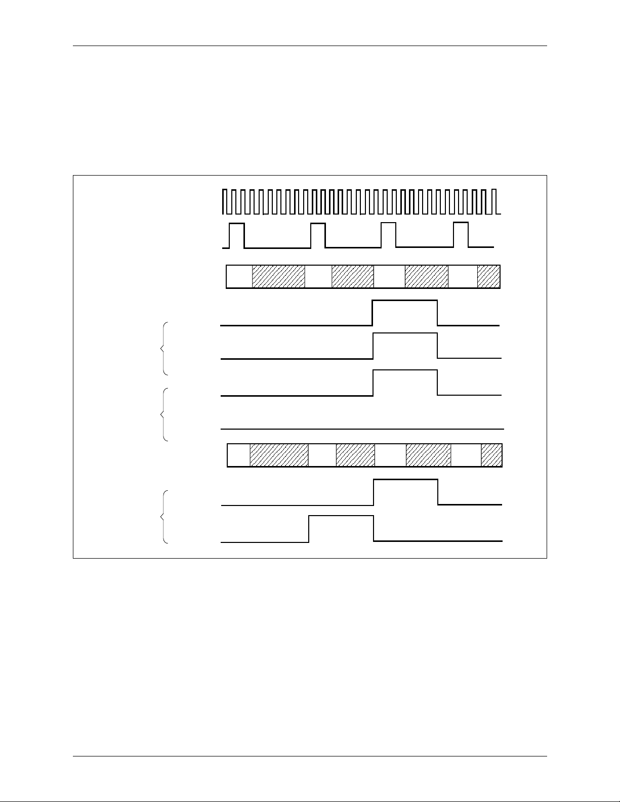
CN8330 2.0 Functional Description
DS3/E3 Framer with 52 Mbps HDLC Controller
Timing for this operation is shown in Figure 2-14.
Illustrated are cases of a good packet received, a packet received with a bad
FCS, and an aborted packet. Each pack et i s shown with one idle flag marking the
end of the packet and the start of the next packet. However, more than one flag
can occur in the serial stream. The output data will contain each occurrence of
idle or abort flags with a pulse on RXBCK/RXGAPCK.
Figure 2-14. PPDL Receiver Timing
RXCLK
RXBCK/
RXGAPCK
Good Packet
RDAT[7:0]
IDLE/FRMCAR
VALFCS/
TXOVH
Data
Data
Flag
2.4 Receiver Operation
Data
Packet
w/Bad FCS
Aborted
Packet
IDLE/FRMCAR
VALFCS/
TXOVH
RDAT[7:0]
IDLE/FRMCAR
VALFCS/
TXOVH
clock input (either DS3CKI or RXCKI depending on FIFEN) and is present
continuously like the transmit byte clock. Nominally there will be one pulse on
RXBCK/RXGAPCK for every eight clock cycles on the receive serial clock.
When an inserted transparency bit must be deleted or DS3/E3 overhead bits
skipped , the RXBCK/RXGAPCK peri od will be lengthe ned by one or more serial
clock cycles. RXBCK/RXGAPCK is present during the reception of FCS octets
and idle flags. The RDAT[7:0], IDLE/F RMCAR, and VALFCS/TXOVH outputs
are valid at least one serial clock cycle period before the rising edge of
RXBCK/RXGAPCK and are valid for at least two serial clock cycle periods after
the falling edge of RXBCK/RXGAPCK.
Data
Abort
Flag
Data
RXBCK/RXGAPCK is generated from the falling edge of the receive serial
100441E Conexant 2-31
Page 54

2.0 Functional Description CN8330
2.4 Receiver Operation DS3/E3 Framer with 52 Mbps HDLC Controller
The parallel interface can be used without transparency bit deletion by setting
the DisPPDL bit in the P PDL Control Register to a 1. In this mode, byte
synchronization in the transmitter and recei ver is achie ved from the M-frame sync
alignment and zeros detected after string s of five ones are not deleted. This allo ws
the byte-wide interface to be used as the data output in normal DS3/E3 mode
rather than the serial output pin. The IDLE/FRMCAR and VALFCS/TXOVH
indications are ignored when o perating in th is mode. Data b y tes are recei v ed with
the same timing relative to RXBCK/RXGAPCK as in HDLC mode. In E3 mode,
190 bytes per frame will be received with byte alignment after the 16 overhead
bits (FAS, A, N, 1100).
The PPDL receiver can be used with a nibble-wide interface for DS3 SMDS
applications if desired. To enable nibb le-wide tran smission, both th e Nibble M ode
Enable and DisPPDL bit controls in the PPDL Control Register should be set to 1.
Received data is available on the least significant nibble of the RDAT[ 7:0] pins
with the same timing relati v e t o RXBCK/RXGAPCK (which now occurs every 4
bits). In nibble mode, the nibbles are received MSB first, with the MSB on
RDAT[3], 2SB on RDAT [2], 1SB on RDAT [1], and the LSB on RDA T[0] . For E3
SMDS applications, the byte-wide interface should be used.
FCS checking can be limited to the first N bytes of the received message by
setting the LimitFCS control bit in the PPDL Control Register. In this mode, the
FCS is checked only on the first N bytes received after the opening flag and then
held until the end of the message. The locall y calcul ated FCS is then compared to
the last two/four bytes in the message to determine if a valid FCS was received.
The desired number N can be from 1 to 16 (a value of 0 gives N = 16) and is
loaded in the FCSC nt[3:0] control field in the PPDL Control Register. This
allows FCS checking only on the header information in a T1 packet voice format.
2.4.9 PPDLONLY Mode
The receiver can be placed in a mode where the entire receive stream is expected
to be data with no DS3/E3 overhead bits inserted. This mode is enabled by
providing a high input on the PPDLONLY input pin. This mode allows the IC to
be used as a high-speed PPDL recei v er an d can be used at an y clock rate u p to the
full 52 MHz capability of the device. This data interface is described in the PPDL
Receiver section of this chapter.
2-32 Conexant 100441E
Page 55
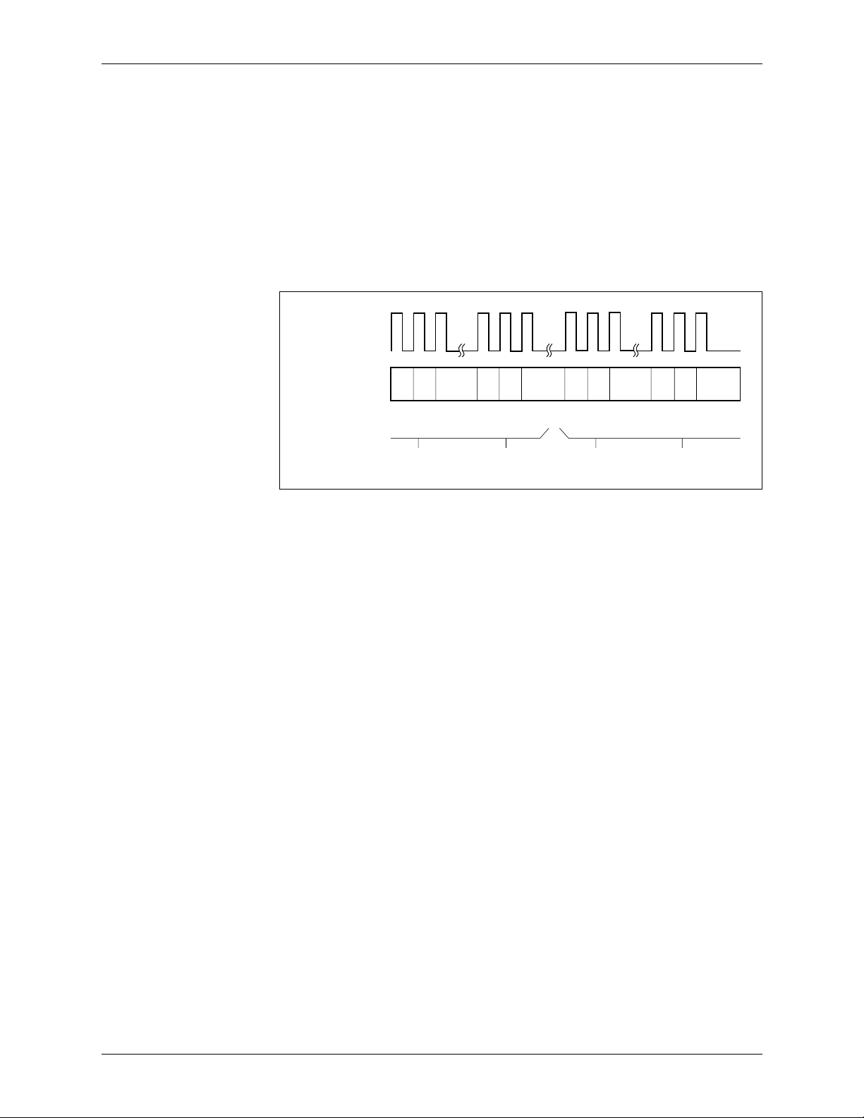
CN8330 2.0 Functional Description
DS3/E3 Framer with 52 Mbps HDLC Controller
2.4.10 Serial C-Bit Output
All received C-bits are output on the CBITO pin on the rising edge of
RXCCK/TZNRZ in DS3 mode. This allows external circuitry to examine
individual C-bits if necessary. The timing is shown in Figure 2-15.
The received N-bits are output on the CBITO pin on the rising edge of
RXCCK/TZNRZ in E3 mode. This allows external circuitry to process the N-bit
if necessary. The relative timing is the same as in DS3 mode except there is only
one N-bit per frame.
Figure 2-15. C-Bit Output Timing
RXCCK/TXNRZ
CBITO
C1 C2 C3 C1 C3 C1 C2
C2
Subframe 1Subframe 7
2.4 Receiver Operation
C3 C1 C2 C3
Subframe 2Subframe 6
100441E Conexant 2-33
Page 56

2.0 Functional Description CN8330
2.5 Monitor Mode for Stand-Al one Operation DS3/E3 Framer with 52 Mbps HDLC Controller
2.5 Monitor Mode for Stand-Alone Operation
Operation without a microprocessor is possible with the MON/MIC* pin tied
high. In this mode of operation, the transmitter is set to M13 format with External
C-Bit Insert [ExtCBit;CR00.2] enabled. E3 mode operation is not available
without a microprocessor . External circuitry must format all of the C-bit locations
to the desired values and present th e m on the CBITI pin in response to the
TXCCK clock output. Proper C-bit ordering can be determined by the
relationship to the input or output M-frame syncs (TDAT[7]/TXSYI or TXSYO).
The parallel data input port for the PP DL transmitter is enabled by setting the
PAREN input high. Setting the CRC32 input high selects the 32-bit CRC mode.
Two special modes are available when in stand-alone operation. When the
PAREN input is high and the PPDLONLY input is low, the byte-wide interfaces
are enabled with transparency bit insertion/deletion disabled. This allows the
CN8330 to be used as a DS3 device with a parallel interface. When the PAREN
input is high and the PPDLONLY input is high, the byte-wide interfaces are
enabled. Transparency bit insertion/deletion is enabled. DS3 framing is disabled.
This allows the CN8330 to be used as a high-speed HDLC formatter. The
transmit serial data stream is available in NRZ format on the RXCCK pin in this
mode.
Alarm generation in this mode is contr olled by t he CS/ALM0 and RD*/ALM1
pins. Setting these pins, as described under Mode Control Register in the
Registers chapter of this document, will enable transmission of the specified
alarm signal (the TxAlm[1:0] bits work identically to the pins).
The receiver will monitor all DS3 maintenance alarms and indications and
provide occu rrences of any alarm on the FRMERR, LCV, PAR, IDLE, YEL, AIS,
OOF, and LOS pins (AD[6:0]). These indications can then be count ed b y e xternal
circuitry for appropriate action. The received data is present on the RXDAT pin
and, if the parallel port is enabled, on the RDAT[7:0] pins. All C-bits are clocked
out on CBITO for external processing.
2-34 Conexant 100441E
Page 57
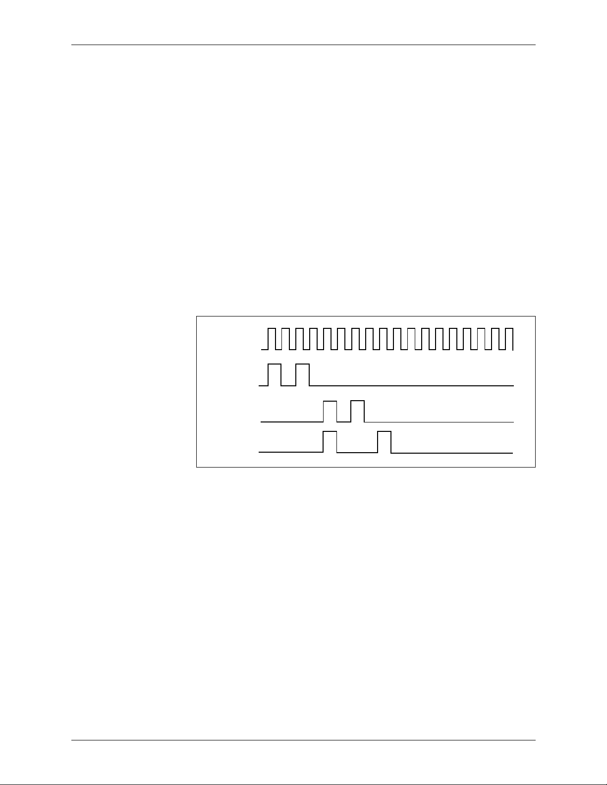
CN8330 2.0 Functional Description
DS3/E3 Framer with 52 Mbps HDLC Controller
2.5.1 DS3 Monitor Mode Error Outputs
If stand-alone monitor mode is selected by tying the MON/MIC* pin high, then
the CN8330 operates without a microprocessor and the eight address/data pins
(AD[7:0]) of the microprocessor interface become DS3 alarm and error
indication outputs (Note that E3 framing is not available in monitor mode).
Outputs are pro vide d for LOS, OOF, AIS, yellow alarm (X-bit lo w or A-b it high),
idle code detect, parity errors, LCVs, and frame bit errors. All indications except
LCV and frame bit errors are level indications and can be counted externall y on a
per M-frame basis, if desired. The frame error output is a pulse for each error in
the M- or F-bit position s and ca n dri ve a counter directly. The LCV output will be
high for every bit position that is an LCV and can be used with the RXCLK
output to facilitate external counting. All indications are active high and can be
used to indicate the presence of the condition without reference to the clock
output. Figure 2-16 illustrates an LCV indication. The LCV indications are
delayed from the pulse inputs due to B3ZS decoding.
Monitor mode is supported only in DS3 mode. Standalone E3 and HDLC
monitor mode is not supported.
Figure 2-16. Monitor Mode Error Indication Timing
2.5 Monitor Mode for Stand-Alone Operation
DS3CKI
RXPOS
RXNEG
AD[6]/LCV
100441E Conexant 2-35
Page 58

2.0 Functional Description CN8330
2.5 Monitor Mode for Stand-Al one Operation DS3/E3 Framer with 52 Mbps HDLC Controller
2-36 Conexant 100441E
Page 59
3
3.0 Registers
For a summary of all registers, refer to the Register Summary section at the end of this chapter.
3.1 Control Registers
0x00—Mode Control Register (CR00)
7 6 5 4 3 2 1 0
LineLp SourceLp TxAlm1 TxAlm0 ExtOvh ExtCBit E3Frm CBitP/DL
LineLp Line Loopback Enab le—Set to enable the loopback in the external direction (back to network).
This loopback connects the received data stream before B3ZS/HDB3 decoding to the
transmitter. All data and overhead bits are looped; and Bipolar Violations (BPVs) are fully
preserved per ANSI standard T1.404. The received data is still presented to all recei ver blocks
and is present on the receiver output pins.
SourceLp Source Loopback Enable—Set to enable the loopback in the internal direction. This loopback
connects the encoded transmitter data and clock directly to the receiver B3ZS/HDB3 decoder.
Transmission of data on the line is not affected by this loopback.
TxAlm1,0 Transmit Alarm Control—Used to control transmission of various alarm signals. In DS3 mode,
the AIS, idle, and yellow alarm signals on the outgoing DS3 stream are controlled as follows:
TxAlm1 TxAlm0 Alarm Action
0 0 Normal, No Alarms Transmitted
0 1 Yellow Alarm (X-bits low) Transmitted
1 0 Idle Code Transmitted
1 1 AIS Transmitted
In E3 mode, the TxAlm0 bit should be set high to transmit the E3 AIS signal and the
TxAlm1 bit is set high to transmit the E3 yellow alarm (A-bit high). TxAlm0 bit has
precedence in E3 mode.
100441E Conexant 3-1
Page 60

3.0 Registers CN8330
3.1 Control Register s DS3/E3 Framer with 52 Mbps HDLC Controller
ExtOvh External Overhead Insert—Set to a 1 to enable insertion of the overhead bits (DS3: X, P, M,
and F or E3: FAS, A, and N) from the transmit serial data stream.
ExtCBit External C-Bit Insert—Used to control insertion of data in the C-bit or N-bit positions of the
transmit data stream. In DS3 mode, the C-bits are controlled as follows:
U
C-Bit Parity Mode Ext. C-Bit Insert C-Bit Source
0 0 Serial Data Stream
01 CBITI Pin
1 0 All C-Bits Internally Generated
1 1 Internal Except CP and FEBE from CBITI Pin
In E3 mode, Exter nal C-Bit Insert controls insertion of da ta in the N-bit position of the E3
data stream. The N-bit will come from the CBITI pin when ExtCBit is high, and from the
terminal data link transmitter when ExtCBit is low.
E3Frm E3 Framing Mode—Enables the E3 mode framing and transmission circuitry. This contr ol bit has
priority over the C-Bit Parity Mode/Enable DLINT bit. Framing insertion and recovery is
performed as specified in ITU–T G.751
CBitP/DL C-Bit Parity Mode/Enable DLINT—Selects which type of framing is present on the
transmitted DS3 signal. If this bit is low, then the basic DS3 framing mode is used. If this
control bit is high, then the C-bit positions are used for the FEBE, FEAC, terminal data link,
path parity, and mode indicator bits as defined in T1.107a-1989. When the E3 framing mode
bit is high, this bit enables interrupts on the DLINT/SOURCELB output pin.
3-2 Conexant 100441E
Page 61
CN8330 3.0 Registers
DS3/E3 Framer with 52 Mbps HDLC Controller
3.1 Control Registers
0x01—Terminal Data Link Control Register (CR01)
This Terminal Data Link Control Register controls functions of the terminal data link as defined in C-bit parity
or E3 mode. If C-bit parity or E3 mode is not selected, the contents of this register are ignored.
7 6 5 4 3 2 1 0
RxTDLIE DisTxTDL TxByte[2] TxByte[1] TxByte[0] TxAbort TxFCS TxMsg
RxTDLIE Receive Terminal Data Link Interrupt Enable—Enables the Receive Terminal Data Link
Interrupt bit [RxTDLI tr;SR02.2] to appear on the
DisTxTDL Disable Transmit Terminal Data Link—Forces the output of the Transmit Terminal Data Link
to all ones.
TxByte[2:0] Byte—A 3-bit pointer to the Transmit Terminal Data Link Message Buffer [TxTDL;0x30–0x37]
address containing the last byte to be transmitted.
TxAbort Abort Message—Causes the data link transmitter to halt the message in progress, send an
abort flag, and then resume transmission of idle flags on the data link.
TxFCS Send Frame Check Sequence—Used to control the transmission of the FCS at the end of a
message block.
TxMsg Send Message—Instructs the transmitter to begin transmission of a message block on the
terminal data link. Setting this bit removes the data link from idle flag transmission mode and
enables interrupts to the controller for data bytes.
DLINT/SOURCELB output pin.
0x02—Status Interrupt Control Register (CR02)
The Status Interrupt Control Register is provi ded to enable or disable individual interrupt sources. To enable an
interrupt from a par ticular source, the c on trol bit corre s ponding to that source must be set high in the interrupt
control register. This enables the interrupt from that source to appear on the CNTINT/LINELB output pin. If a
source has its interrupt control bit set low, then interrupts from this counter will be masked from appearing on
CNTINT/LINELB.
7 6 5 4 3 2 1 0
SR6IE RxFEACIE LCVCtrIE FEBECtrIE PthCtrIE FerrCt rIE DgrCtrIE ParCtrlE
SR6IE Shadow Register Interrupt Enable—A control bit that allows interrupts fro m the Shadow
Status Register [SR06;0x16] to appear on the CNTINT/LINELB output pin.
RxFEACIE Receive FEAC Interrupt Enable—A control bit that allows interrupts from the FEAC receiver
to appear on the DLINT/SOURCELB output pin when in C-bit parity mode.
LCVCtrIE Line Code Violation Counter Interrupt Enable—A control bit that allows interrupts from the
DS3/E3LCV Counter [SR12,SR13;0x25,0x26] to appear on the CNTINT/L INE LB out put pi n.
FEBECtrIE FEBE Event C ou nter Interrupt Enable—A control bit that allows interrupts fro m the DS3
FEBE Event Counter [SR11;0x24] to appear on the CNTINT/LINELB output pin.
PthCtrIE Path Parity Error Counter Interrupt Enable—A control bit that allows interrupts from the Path
Parity Error Counter [SR10;0x23] to appear on the CNTINT/LINELB output pin.
FerrCtrIE Frame Error Counter Interrupt Enable—A control bit that allows interrupts from the Frame
Error Counter [SR09;0x22] to appear on the CNTINT/LINELB output pin.
100441E Conexant 3-3
Page 62
3.0 Registers CN8330
3.1 Control Register s DS3/E3 Framer with 52 Mbps HDLC Controller
DgrCtrIE Disagreement Counter Interrupt Enable—A control bit that allows interrupts from the D S3
Disagreement Counter [SR08;0x21]to appear on the CNTINT/LINELB output pin.
ParCtrIE Parity Error Counter Interrupt Enable—A control bit that allows interrupts from the DS3
Parity Error Counter [SR07;0x20]to appear on the CNTINT/LINELB output pin.
0x03—Transmit FEAC Channel Byte (CR03)
7 6 5 4 3 2 1 0
TxFEAC[7] TxFEAC[6] TxFEAC[5] TxFEAC[4] TxFEAC[3] TxFEAC[2] TxFE AC[1] TxFEAC[0]
TxFEAC[7:0] T ransmit FEAC Channel Message Byte—If the mode is set to C-bit parity, this register will be
used as the data byte for the transmit FEAC channel transmitter. When this byte is in the form
'0xxxxxx0' it is transmitted after every flag. If there is a one in either the most significant or
least significant bit of this register, all ones (idle) will be transmitted on the data link a nd
interrupts from this source will be disabled. Writing to this register clea rs the Transmit FEAC
Channel Interrupt bit [TxFEACItr;SR02.1] in the Data Link Interrupt Status Register
[SR02;0x12].
0x04—Feature Control Register (CR04)
The Feature Control Register is provided to enable or disable miscellaneous features in the CN8330.
7 6 5 4 3 2 1 0
TstEqSel AMI/LCV2 DisEnc DisLCV/Ferr ParaEn FEBEC[3] FEBEC[2] FEBEC[1]
TstEqSel Test Equipment Feature Select—Set high to enable direct access to the B3ZS/HDB3 encoder
and to enable insertion of LCVs via the TDAT[5]/TXENCI and TDAT[4]/LCVERRI pins,
respectively. Normal operation of the transmitter is enabled when this bit is low.
AMI/LCV2 AMI Mode/LCV Type 2—Set high to enable AMI outputs on TXPOS and TXNEG (no
B3ZS/HDB3 encoding). If the Test Equipment Feature Select bit is also set high, then this bit
selects the type of LCV errors created when TDAT[4]/LCVERRI is active (see Table 2-1).
DisEnc Disable B3ZS/HDB3 Encoding—Set high to disable the B3ZS/HDB3 encoder circuit and
provide a unipolar NRZ output instead of B3ZS/HDB3 encoded output pulses. The unipolar
output appears at the TXPOS pin and the
(see Table 2-1).
DisLCV/Ferr Disable Saturation of Line Code Violation/Frame Errors—Set to allow the LCV and Frame
Error Counters to continue counting when the maximum count has been received without
enabling the respective interrupt. This is for use with the carry output indications for these
counters as described in DS3/E3 Error Counters section in this chapter.
DS3/E3 input clock is available on the TXNEG pin
ParaEn Parallel Data Enable—Set high to enable the PPDL transmitter and receiver as the source and sink
for data. Eight-bit data bytes on the TDA T[ 7:0] and RDAT[7:0] buses for the PPDL transmitter and
receiver are provided. In E3 mode, the overhead field is also altered as described in Framing-Bit
Generation under the Transmitter Operation section in the Functional Description chapter. If this
control bit is low, the TDAT[6]/TXDATI and RXDAT data lines are the data input and output,
respectively, for the DS3/E3 stream.
3-4 Conexant 100441E
Page 63
CN8330 3.0 Registers
DS3/E3 Framer with 52 Mbps HDLC Controller
FEBEC[3:1] FEBE Pattern Bit Field—Set to the 3-bit sequence that is to be sent each time a FEBE
3.1 Control Registers
indication is to be transmitte d in C-bit parity mode. This pattern is automatically transmitte d
when the receiv er detec ts an F-bit or path parit y error . The pattern must be anythi ng other than
all ones to indicate a FEBE to the far end. An all-o nes pattern will disable FEBE transmission
and should not be used for any other purpose.
0x05—PPDL Control Register (CR05)
The PPDL Control Register is provided to control the mode of operation of the PPDL transmitter and receiver.
7 6 5 4 3 2 1 0
FCSCnt[3] FCSCnt[2] FCSCnt[1] FCSCnt[0] LimitFCS CRC32 DisPPDL Nibble
FCSCnt[3:0] Frame Check Sequence Calculation Count—Determine s the number of bytes over which the
FCS is to be calculated. The number of bytes for calculation can be from 1 to 16 (a value of 0
results in 16 bytes of calculation).
LimitFCS Limit Frame Check Sequence Calculation—Set to enable FCS calculation only on the first N
bytes of an HDLC frame w h ere N is dete rmined b y the FCS C alculat ion C ount field. If this bit
is low, the FCS will be calculated over all transmitted bytes.
CRC32 32-Bit Cycle Redundancy Check—Set high to enable 32-bit CRC generation and ch ecking on
the PPDL. If this bit is low, then 16-bit CRC generation and checking is e nabled.
DisPPDL Disable PPDL Transparency Bit—Set high to disable insertion and removal of HDLC
transparency bits in the PPDL transmitter and receiver. If this control bit is low, then normal
insertion and removal of HDLC transparency bits will occur.
Nibble Nibble Mode Enable—Set to enable the nibble mode interface to the PPDL transmitter and
receiver f or use in DS3 SMDS/ 802.6 appli cations. T he Disab le P PDL Transparency bit should
be set high when nibble mode is enabled.
100441E Conexant 3-5
Page 64
3.0 Registers CN8330
3.2 Status Registers DS3/E3 Framer with 52 Mbps HDLC Controller
3.2 Status Registers
There are six Status Registers: five for DS3/E3 status and one to indicate the version number of the IC. Also
included is a shadow register for the DS3/E3 maintenance status to latch status indications until read. The
contents of these registers are described here and summarized in the Register Summary at the end of this
section. The status signals are contained in latches and are applied to the controller data bus on the appropriate
read command from the controller. The active state of all bits in the Status Registers is high.
0x10—DS3/E3 Maintenance Status Register (SR00)
The DS3/E3 Maintenance Status Register contains the major DS3/E3 maintenance indicators. Alarm detection
details can be found in Alarm Detection in the Receiver Operation section of the Functional Description
chapter.
7 6 5 4 3 2 1 0
ReFrm FrmtID1 FrmtID0 IdleDet YelDet AISDet OOFAlm LOSAlm
ReFrm Reframe In Progress—Set while the framing circuit is searching for a valid framing pattern in
either DS3 or E3 modes.
FrmtID1,0 F ormat Identification—Identifies the incoming format based on the contents of the appli cation
ID channel contained in the first C-bit of subframe 1. This bit pair will be set to 00 to indicate
M13 format, 01 to indicate C-bit parity format, and 10 to indicat e Syntran format. In E3 mode,
these bits are meaningless and should be ignored.
IdleDet Idle Code Detect—Set if there is valid framing and parity, the three C-bits in subframe 3 are
zero, both X-bits are equal, and the pa yload contains a 1100... pattern starting with an 11 after
each overhead bit in DS3 mode. This bit will be low in E3 mode since there is no defined E3
idle signal.
YelDet Yellow Alarm Detect—Set for one M-frame interval when both X-bits ar e low in the previous
M-frame in DS3 mode. This bit is set when the recei v ed A-bit is high in E3 mod e. This bit will
not go active if LOSAlm, OOFAlm, or AISDet are active.
AISDet Alarm Indication Signal Detect—Set if there is valid framing and parity, all C-bits are 0, both
X-bits are equal, and the payload contains a 1010... pattern starting with a one after each
overhead bit in DS3 mode. This bit is set when an unframed all-ones signal is received in E3
mode.
OOFAlm Out of Frame Alarm—Set when any 3 out of 16 consecutive F framing bits are in error or
when 2 out of 3 consec uti v e M frame s have errors in the M bit positions in DS3 mode. This b it
is set when four consecutive FAS errors have been received in E3 mode. This condition w ill
initiate a reframe.
LOSAlm Loss-Of-Signal Alarm—Indicates that the received signal prior to B3ZS/HDB3 decoding has
been low for 175 ± 75 clock cycles. This indicates that the DS3/E3 line signal has been lost.
This signal is set as soon as the loss-of-signa l condit ion is det ected and i s cleared wh en at least
33 percent (25 percent in E3 mode) one's density is achieved for 175 ± 75 clock cycles
3-6 Conexant 100441E
Page 65
CN8330 3.0 Registers
DS3/E3 Framer with 52 Mbps HDLC Controller
3.2 Status Registers
0x11—Counter Interrupt Status Register (SR01)
The Counter Interrupt Status Register contains status information about active interrupts needing service from
the controller . This re gister needs to be read by the contro ller upon recei ving a counter interrupt to determine the
source of the interrupt. The interrupt indications are active high in the regist er and are available even if they are
not enabled to be visible on the CNTINT/LINELB output pin. Servicing will clear this interrupt indication as
described in Microprocessor Interrupts in the Microprocessor Interface section in the Functional Description
chapter. Counter operation is discussed in DS3/E3 Error Counters in the Status R e g ist ers sect io n of t his chapt er.
NOTE(S): Rsvd bits in Control Registers must be set to zero.
7 6 5 4 3 2 1 0
Rsvd ShdwItr LCVCtrItr FEBECtrItr PthCtrItr FerrCtrItr DgrCtrItr ParC trlltr
ShdwItr Shadow Status Register Interrupt—Set if any of the bits in the Shadow Status Register get set.
This bit is cleared by reading the Shadow Status Register [SR06;0x16].
LCVCtrItr LCV Counter Interrupt—Set high on an LCV error counter roll-over or saturation. The LCV
Counter Interrupt Enable bit [LCVCtrIE;CR02.5] determines the status of the counter. This bit
is cleared when this status register is read.
FEBECtrItr FEBE Event Counter Interrupt—Set high if the FEBE event count er has either roll ed o v er or is
saturated. The FEBE Event Counter Interrupt Enable [FEBECtrIE;CR02.4] determines the
status of the counter. This bit is cleared when this status register is read.
PthCtrItr Path Parity Error Counter Interrupt—Set high if the path parity error counter has either rolled
over or is saturated. The Parity Error Counter Interrupt Enable bit [PthCtrIE.CR02.3]
determines the status of the counter. This bit is cleared when this status register is read.
FerrCtrItr Frame Error Counter Interrupt—Set high when the frame error counter has either rolled over
or is saturated. The Frame Error Counter Interrupt Enable [FerrCtrIE;CR02.2] determines the
status of the counter. This bit is cleared when this status register is read.
DgrCtrItr Disagreement Counter Interrupt—Set high if the disagreement counters have either rolled over
or are saturated. The Disagreement Counter Interrupt Enable bit [DgrCtrIE;CR02.1]
determines the status of the counter. This bit is cleared when this status register is read.
ParCtrItr Parity Error Counter Interrupt—Set high if the parity error counter has either rolled over or is
saturated. The Parity Error Counter Interrupt Enable bit [ParCtrIE;CR02.0] determines the
status of the counter. This bit is cleared when this status register is read.
100441E Conexant 3-7
Page 66
3.0 Registers CN8330
3.2 Status Registers DS3/E3 Framer with 52 Mbps HDLC Controller
0x12—Data Link Interrupt Status Register (SR02)
The Data Link Interrupt Status Register contains information about active data link interrupts needing service
from the controller. The controller determines the source of the data link interrupt by reading this register. The
interrupt indications are active high and can be from four sources: Transmit FEAC Channel, Receive FEAC
Channel, Transmit Terminal Data Link, and Receive Terminal Data Link. Servicing an interrupt clears the
indication in this register.
NOTE(S): Rsvd bits in Control Registers must be set to zero.
7 6 5 4 3 2 1 0
Rsvd Rsvd Rsvd Rsvd TxTDLItr RxTDLItr TxFEACItr RxFEACltr
TxTDLItr Transmi t Terminal Data Link Interrupt—Set high when the transmitter has latched the present
set of controls in the Terminal Data Link Control Re gister [C R01; 0x01] and is ready for a ne w
set. Writing the Terminal Data Lin k Control Register clears this interrupt.
RxTDLItr Receive Terminal Data Link Interrupt—Set high by the Receive Data Link circuitry. Reading
the Terminal Data Link Status Register clears this interrupt.
TxFEACItr Transmit FEAC Channel Interrupt—Set high indicating that the transmitter is ready for a new
byte to be written to the Transmit FEAC Channel Byte Register. Writing the Transmit FEAC
Channel Byte clears this interrupt.
RxFEACItr Receive FEAC Channel Interrupt—Set high when a FEAC message byte has been received
and placed in the Receive FEAC Channel Byte Register. Reading the Receive FEAC Channel
Byte Register clears this interrupt.
0x13—Receive FEAC Channel Byte (SR03)
7 6 5 4 3 2 1 0
RxFEAC[7] RxFEAC[6] RxFEAC[5] RxFEAC[4] RxFEAC[3] RxFEAC[2] RxFEAC[1] RxFEAC[0]
RxFEAC[7:0] Receive FEAC Channel Message Byte—If the incoming format is C-bit parity, this register
contains the received byte from the bit-oriented receive FEAC channel. The receive FEAC
channel is only defined in C-bit parity format. Receive FEAC message reception is described
in RxFEAC Channel Reception in the Receiver Operation section of the Functional
Description chapter. This byte is meaningless in E3 mode and should be ignored.
3-8 Conexant 100441E
Page 67
CN8330 3.0 Registers
DS3/E3 Framer with 52 Mbps HDLC Controller
3.2 Status Registers
0x14—Terminal Data Link Status Register (SR04)
The Terminal Data Link Status Register contains the status indications for the LAPD receiver of the terminal
data link. This data link is onl y defined in C-bit parity or E3 modes. Terminal data link reception is described in
the Receiver Operation section of the Functional Description chapter.
Terminal data link receiver functions include FCS checking, transparency bit removal, and flag detection.
LAPD messages may be read from the Receive Terminal Data Link Message Buffer [RxTDL;0x40–0x47], and
require the use of the DLINT/SOURCELB interrupt to synchronize the transfer of message data between the
receiver and microprocessor.
NOTE(S): Reserved bits in Control Registers must be set to zero.
7 6 5 4 3 2 1 0
Reserved Reserved RxByte[2] RxByte[1] RxByte[0] RxIdle BadFCS RxAbort
RxByte[2:0] Byte Pointer—A 3-bit pointer to the last location written in the Receive Terminal Data Link
Message Buffer.
RxIdle Idle Code Received—Indicates that an idle flag sequence (01111110) was received on the
terminal data link.
BadFCS Bad FCS—Set when an erroneous FCS was received at the end of a message or an idle flag is
received that is not byte aligned.
RxAbort Abort Flag Received—Set if an abort sequence (seven consecutive ones) is received on the
terminal data link.
0x15—Part Number/Hardware Version Register (SR05)
The Part Number/Hardware Version Register contains a part number in the upper nibble and a version number
in the lower nibble. This register is provided so that the processor will know what version of the CN8330 is
present. This enab l es loadin g of v ersi on-specific software, if ne eded. T he part number for t he C N8330 fr amer is
0000. The version number is indicated below and will be incremented with any change in circuitry within the
IC.
7 6 5 4 3 2 1 0
Part[3] Part[2] Part[1] Part[0] Ver[3] Ver[2] Ver[1] Ver[0]
U
Conexent Part Number
CN8330EPJ UGA-330-1 0x01
CN8330EPJB UGA-330-2 0x02
CN8330EPJC/CN8330EPFC — 0x03
CN8330EPJD/CN8330EPFD — 0x04
Obsolete Base
Number
Part
2
Hex Value
100441E Conexant 3-9
Page 68
3.0 Registers CN8330
3.2 Status Registers DS3/E3 Framer with 52 Mbps HDLC Controller
0x16—Shadow Status Register (SR06)
The Shadow Status Register contains copies of the five least significant bits of the DS3/E3 Maintenance Status
Register [SR00;0x10]. Whenever a status indication appears in the DS3/E3 Maintenance Status Register, the
corresponding bit is also set in the Shadow Status Register. The bits in this Shadow Status Register are latched
and held until the controller reads the register. This register provides a way to monitor transient occurrences of
alarm indications without continuously polling the DS3/E3 Maintenance Status Register. An additional bit not
contained in the DS3/E3 Maint enance Statu s Regist er is All-Ones Detect . If the shado w i nterrupt is enabled, any
occurrence of an indication in bits 0 through 4 will cause an active low interrupt to occur on the
CNTINT/LINELB pin .
NOTE(S): Rsvd bits in Control Registers must be set to zero.
7 6 5 4 3 2 1 0
Rsvd Rsvd ShdwAll1 ShdwIdle ShdwYel ShdwAIS ShdwOOF ShdwLOS
ShdwAll1 Shadow All-Ones Detect—Set whenever an unframed all-ones signal has been detected in
either DS3 or E3 mode.
ShdwIdle Shadow Idle Code Detect—Set if there is valid framing and parity , the three C-bits in subframe
3 are zero, both X-bits are equal, and the payload contains a 1100... pattern starting with a 11
after each o ve rhead bit i n DS3 mode. This bit wil l be low in E3 mode since there is no defined
E3 idle signal.
ShdwYel Shadow Yellow Alarm Detect—Set for one M-frame interval when both X-bits are low in the
previous M-frame in DS3 mode. This bit is set when the received A-bit is high in E3 mode.
ShdwAIS Shado w Alarm Indic ation Signal Detect —Set if there is valid framing and parity, all C-bits are
0, both X-bits are equal, and the payload contains a 1010... pattern starting with a one after
each overhead bit in DS3 mode. This bit is set when an unframed all-ones signal i s received in
E3 mode.
ShdwOOF Shadow Out of Frame—Set when any 3 out of 16 consecutive F framing bits are in error or
when 2 out of 3 conse cuti ve M -frames ha v e errors in the M-bit p ositions i n DS3 mode. Th is bit
is set when four consecutive FAS errors have been received in E3 mode. This condition w ill
initiate a reframe.
ShdwLOS Shadow Loss-of-Signal Alarm—Indicates that the received signal prior to B3ZS/HDB3
decoding has been low for 175 ± 75 clock cycles. This indicates that the CN8330 line signal
has been lost. This sign al is set as soon as t he loss-of-si gnal condi tion is det ected and is cleared
when at least 33percent (25 percent in E3 mode) one's density is achieved for 175 ± 75 clock
cycles.
3-10 Conexant 100441E
Page 69

CN8330 3.0 Registers
DS3/E3 Framer with 52 Mbps HDLC Controller
3.2 Status Registers
0x20–0x26—DS3/E3 Error Counters
There are six error counters for DS3/E3 errors located at addresses 0x20–0x26. All are 8-bit counters with the
exception of the DS3 Disagreement [SR08;0x21] and DS3/E3 LCV Counters [SR12,SR13;0x25,0x26]. The
8-bit counters indicate 0 through 255 counts of a particular error. If the interrupt for a particular counter is not
enabled, the counter will saturate at 255 when more than 255 counts of that error are received and the saturation
indication will appear in the Counter Interrupt Status Register [SR01;0x01]. The saturation indication and the
counter will be cleared when the counter is read. If the interrupt for a particular counter is enabled in the
Interrupt Control Register [CR02; 0x02], then the counter will not saturate but will roll over and continue
counting from zero. An interrupt will be generated on the CNTINT/LINELB output pin and will appear in the
Counter Interrupt Status Register when the counter rolls over to a count of zero. The interrupt will be cleared
when the Counter Interrupt Status Register is read.
The only valid counters in E3 mode are the DS3/E3 LCV and Frame Error Counters. The DS3/E3 Frame
Error Counter [SR09;0x22] counts each occurrence of an incorrect pattern in the 10-bit FAS.
All counters are cleare d when read by the microprocessor. The interrupt indication for a particular counter i s
also cleared when the counter is read. Both nibbles of the DS3 Disagreement Counter [SR08;0x21] are cleared
when address 0x21 is read. Each byte of the DS3/E3 LCV Counter is cleared separately when it is read.
Software should read the low byte first and then the high byte to prevent any missed counts. All counters are
designed so that errors occurring during reads by the microprocessor will not be missed or double-counted. All
counters except for LCV and Frame Error are frozen during an OOF condition. The LCV and Frame Error
Counters continue counting errors during an OOF condition. Both counters also have ripple carry outputs
available when the PPDL port is not in use. These outputs are on the RDAT[5] and IDLE pins, respectively.
Saturation of these two counters can be disabled without enabling the respective interrupts by setting the
Disable Saturation of LCV/Frame Errors bit [DisL CV/Ferr;CR04.4] in the Feature Control Register
[CR04;0x04]. This allows external enlargement of these counters by use of the ripple carry outputs without
interruption of the micro processor.
0x20—DS3 Parity Error Counter (SR07)
7 6 5 4 3 2 1 0
DS3ParCtr[7] DS3ParCtr[6] DS3ParCtr[5] DS3ParCtr[4] DS3ParCtr[3] DS3ParCtr[2] DS3ParCtr[1] DS3ParCtr[0]
DS3ParCtr[7:0] DS3 Parity Error Counter—Increments for each M-frame in which the calcula ted pari ty of t he
received data bits of the previous M-frame do not match the received parity bits. If the two
parity bits are different this counter will increment.
100441E Conexant 3-11
Page 70
3.0 Registers CN8330
3.2 Status Registers DS3/E3 Framer with 52 Mbps HDLC Controller
0x21—DS3 Disagreement Counter (SR08)
The DS3 Disagreement Counter consists of two 4-bit counters. Both counters indicate 0 through 15 counts of
disagreements in either the two X (yellow alarm) bits or the two P (parity) bits. If the interrupt is not enabled,
the counters saturate at 15 when more than 15 counts are received. Saturation of either 4-bit counter will
generate a disagreement counter interrupt indication in Counter Interrupt Status Register [SR01;0x11]. If the
disagreement interrupt is enabled, the counters will roll over and continue counting after 15 error counts and
generate an interrupt in Counter Interrupt Status Register and on the CNTINT/LINELB pin.
7 6 5 4 3 2 1 0
ParDgrCtr[3] ParDgrCtr[2] ParDgrCtr[1] ParDgrCtr[0] XDgrCtr[3] XDgrCtr[2] XDgrCtr[1] XDgrCtr[0]
ParDgrCtr[3:0] Parity-Bit Disagreement Counter—If the two P-bits in an M-frame are in disagreement, the
P-bit disagre ement counter nibble will be incremented.
XDgrCtr[3:0] X-Bit Disagreement Counter—If the two X-bits in an M-frame are in disagreement (due to
line errors), the X-bit disagreement counter nibble will be incremented.
0x22—DS3/E3 Frame Error Counter (SR09)
7 6 5 4 3 2 1 0
FerrCtr[7] FerrCtr[6] FerrCtr[5] FerrCtr[4] FerrCtr[3] FerrCtr[2] FerrCtr[1] FerrCtr[0]
FerrCtr[7:0] Frame Error Counter—Increments with each error in the M- or F-bit framing pattern in DS3
mode and with each error in the FAS pattern in E3 mode. Errors are still counted during an
OOF condition (OOFAlm = 1).
0x23—DS3 Path Parity Error Counter (SR10)
7 6 5 4 3 2 1 0
DS3PthCtr[7] DS3PthCtr[6] DS3PthCtr[5] DS3PthCtr[4] DS3PthCtr[3] DS3PthCtr[2] DS3PthCtr[1] DS3PthCtr[0]
DS3PthCtr[7:0] DS3 Path Parity Error Counter—Increments for each M-frame in which the calculated parity
of the received data bits of the previous M-frame do not match a majority vote of the three
received CP bits (C-bits in subframe 30).
3-12 Conexant 100441E
Page 71

CN8330 3.0 Registers
DS3/E3 Framer with 52 Mbps HDLC Controller
3.2 Status Registers
0x24—DS3 FEBE Event Counter (SR11)
7 6 5 4 3 2 1 0
DS3FEBE[7] DS3FEBE[6] DS3FEBE[5] DS3FEBE[4] DS3FEBE[3] DS3FEBE[2] DS3FEBE[1] DS3FEBE[0]
DS3FEBE[7:0] DS3 FEBE Event Counter— Increments for each M-frame where any C-bit in subframe 4
is zero.
0x25,0x26—DS3/E3 LCV Counter—Low and High Bytes (SR12,SR13)
The DS3/E3 LCV Counter is a 16-bit counter with the low byte located at address 0x25 and the high byte
located at address 0x26. I f the interrupt for the DS3/E3 LCV Count er is n ot enabled, the counter wi l l satu ra te at
65535 and the saturation indication will appear in the Counter Interrupt Status Register [SR01;0x11]. If the
interrupt is enabled, the counter will roll over and continue counting as for the 8-bit counters. In DS3 mode, this
counter increments upon each occurrence of a Bipolar Violation (BPV) and each sequence of three or more
zeroes. In E3 mode, it increments only upon each occurrence of an LCV per ITU-T O.161 (an LCV is defined
as two consecutive BPVs of the same polarity).
7 6 5 4 3 2 1 0
LCVCtr[7] LCVCtr[6] LCVCtr[5] LCVCtr[4] LCVCtr[3] LCVCtr[2] LCVCtr[ 1] LCVCtr[0]
15 14 13 12 11 10 9 8
LCVCtr[15] LCVCtr[14] LCVCtr[13] LCVCtr[12] LCVCtr[11] LCVCtr[10] LCVCtr[9] LCVCtr[8]
100441E Conexant 3-13
Page 72
3.0 Registers CN8330
3.3 Memory Registers DS3/E3 Framer with 52 Mbps HDLC Controller
3.3 Memory Registers
0x30–0x37—Transmit Terminal Data Link Message Buffer (TxTDL)
The Transmit Terminal Data Link Message Buffer locations are loaded with the message bytes t o be sent on the
terminal data link in response to the Transmit Terminal Data Link In terrupt.
7 6 5 4 3 2 1 0
TxTDL[7] TxTDL[6] TxTDL[5] TxTDL[4] TxTDL[3] TxTDL[2] TxTDL[1] TxTDL[0]
0x40–0x47—Receive Terminal Data Link Message Buffer (RxTDL)
The Receive Terminal Data Link Message Buffer contains the message byte s recei v ed on the terminal data link.
The Receive Terminal Data Link Interrupt indicates the presence of data in the receive buffer.
7 6 5 4 3 2 1 0
RxTDL[7] RxTDL[6] RxTDL[5] RxTDL[4] RxTDL[3] RxTDL[2] RxTDL[1] RxTDL[0]
3-14 Conexant 100441E
Page 73
3
100441E
Conexant
3.4 Register Summary
Table 3-1. Register Overview
ADDR
0x00 CR00 R/W LineLp SourceLp TxAlm1 TxAlm0 ExtOvh ExtCBit E3Frm CBitP/DL
0x01 CR01 R/W RxTDLIE DisTxTDL TxByte[2] TxByte[1] TxByte[0] TxAbort TxFCS TxMsg
0x02 CR02 R/W SR6IE RxFEACIE LCVCtrIE FEBECtrIE PthCtrIE FerrCtrIE DgrCtrIE ParCtrIE
0x03 CR03 R/W TxFEAC[7] TxFEAC[6] TxFEAC[5] TxFEAC[4] TxFEAC[3] TxFEAC[2] TxFEAC[1] TxFEAC[0]
0x04 CR04 R/W TstEqSel AMI/LCV2 DisEnc DisLCV/Ferr ParaEn FEBEC[3] FEBEC[2] FEBEC[1]
0x05 CR05 R/W FCSCnt[3] FCSCnt[2] FCSCnt[1] FCSCnt[0] LimitFCS CRC32 DisPPDL Nibble
Table 3-2. Status Register s (1 of 2)
Register
Label
Read
Write
7 6 5 4 3 2 1 0
Bit Number
DS3/E3 Framer with 52 Mbps HDLC Controller
CN8330
3-15
ADDR
0x10 SR00 R ReFrm FmtID1 FmtID0 IdleDet YelDet AISDet OOFAlm LOSAlm
0x11 SR01 R Rsvd ShdwItr LCVCtrItr FEBECtrItr PthCtrItr FerrCtrItr DgrCtrItr ParCtrItr
0x12 SR02 R Rsvd Rsvd Rsvd Rsvd TxTDLItr RxTDLItr TxFEACItr RxFEACItr
0x13 SR03 R RxFEAC[7] RxFEAC[6] RxFEAC[5] RxFEAC[4] RxFEAC[3] RxFEAC[2] RxFEAC[1] RxFEAC[0]
0x14 SR04 R Rsvd Rsvd RxByte[2] RxByte[1] RxByte[0] RxIdle BadFCS RxAbort
0x15 SR05 R Part[3] Part[2] Part[1] Part[0] Ver[3] Ver[2] Ver[1] Ver[0]
0x16 SR06 R Rsvd Rsvd ShdwAll1 ShdwIdle ShdwYel ShdwAIS ShdwOOF ShdwLOS
0x20 SR07 R DS3ParCtr[7] DS3ParCtr[6] DS3ParCtr[5] DS3ParCtr[4] DS3ParCtr[3] DS3ParCtr[2] DS3ParCtr[1] DS3ParCtr[0]
Register
Label
Read
Write
7 6 5 4 3 2 1 0
Bit Number
3.4 Register Summary
Page 74
3-16
Table 3-2. Status Register s (2 of 2)
3.4 Register Summary
ADDR
0x21 SR08 R ParDgrCtr[3] ParDgrCtr[2] ParDgrCtr[1] ParDgrCtr[0] XDgrCtr[3] XDgrCtr[2] XDgrCtr[1] XDgrCtr[0]
0x22 SR09 R FerrCtr[7] FerrCtr[6] FerrCtr[5] FerrCtr[4] FerrCtr[3] FerrCtr[2] FerrCtr[1] FerrCtr[0]
0x23 SR10 R DS3PthCtr[7] DS3PthCtr[6] DS3PthCtr[5] DS3PthCtr[4] DS3PthCtr[3] DS3PthCtr[2] DS3PthCtr[1] DS3PthCtr[0]
0x24 SR11 R DS3FEBE[7] DS3FEBE[6] DS3FEBE[5] DS3FEBE[4] DS3FEBE[3] DS3FEBE[2] DS3FEBE[1] DS3FEBE[0]
0x25 SR12 R LCVCtr[7] LCVCtr[6] LCVCtr[5] LCVCtr[4] LCVCtr[3] LCVCtr[2] LCVCtr[1] LCVCtr[0]
0x26 SR13 R LCVCtr[15] LCVCtr[14] LCVCtr[13] LCVCtr[12] LCVCtr[11] LCVCtr[10] LCVCtr[9] LCVCtr[8]
Table 3-3. Transmit Terminal Data Link Message Buffer
Conexant
ADDR
0x30–0x37 TxTdl R/W TxTDL[7] TxTDL[6] TxTDL[5] TxTDL[4] TxTDL[3] TxTDL[2] TxTDL[1] TxTDL[0]
Table 3-4. Rec eive Terminal Data Link Message Buffer
ADDR
Register
Label
Register
Label
Register
Label
Read
Write
Read
Write
Read
Write
7 6 5 4 3 2 1 0
7 6 5 4 3 2 1 0
7 6 5 4 3 2 1 0
Bit Number
Bit Number
Bit Number
DS3/E3 Framer with 52 Mbps HDLC Controller
0x40–0x47 RxTdl R/W RxTDL[7] RxTDL[6] RxTDL[5] RxTDL[4] RxTDL[3] RxTDL[2] RxTDL[1] RxTDL[0]
100441E
CN8330
Page 75
4.0 Mechanical/Electrical Specifications
4.1 Timing Requirements
Table 4-1 and Figure 4-1 illustrate the timing requirements for the microprocessor
interface. The parameter t
This clock signal is used in the read circuit of the microprocessor to ensuring no
status events are missed and that counter values are accurately read.
Read operation requires the read strobe to be low for three t
ensuring that changing status and error counts are properl y proc essed. If a gapped
clock is applied to the circuit, it is sufficient to allow three receive clock cycles
between read strobes to allow a latching circuit to clear in the microprocessor
interface.
Table 4-1. Mic r oprocessor Interface Timing (1 of 2)
4
is the period of the r ecei ve DS 3/E3 clo ck (DS3CKI).
cyc
clock cycles
cyc
Symbol Parameter Min. Typical Max. Units
t
as
t
cale
t
ah
t
rwa
t
adwrh
t
adrdl
(Read Operation)
t
wrw
(Write Operation) WR* Pulse Width 100 ——ns
t
wrw
t
rdd
t
rdh
Address Setup bef ore ALE Low 7 ——ns
Controller ALE Pulse Width 34 ——ns
Address Hold after ALE Lo w 10 ——ns
RD*/WR* High to ALE High 10 ——ns
Address/Select to WR* High 117 ——ns
Address/Select to RD* Lo w 17 ——ns
RD* Pulse Width
RD* Low to Data Available ——30 ns
Read Data Hold Time
(1)
(2)
3 × t
cyc
3 ——ns
——ns
100441E Conexant 4-1
Page 76
4.0 Mechanical/Electrical Specifications CN8330
4.1 Timing Requirements DS3/E3 Framer with 52 Mbps HDLC Controller
Table 4-1. Mic r oprocessor Interface Timing (2 of 2)
Symbol Parameter Min. Typical Max. Units
t
clcl
t
ds
t
dh
t
sh
ALE Low to RD*/WR* Low 10 ——ns
Data Stable Before WR* High 25 ——ns
Data Hold after WR* High 10 ——ns
Address/Select Hold after RD*/WR* Low 110 ——ns
— Controller Port Cycle Time 154 ——ns
NOTE(S):
(1)
T
= Period of clock connected to the DS3CKI pin.
cyc
(2)
The external address/data bus capacitance will incr ease the data hold time if the bus remains undriven.
Figure 4-1. Microprocessor Interface Timing
CS
t
RD*/WR*
AD[7:0]
ALE
t
cale
adwrh
t
adrdl
t
rdd
t
as
t
ah
t
clcl
t
wrw
t
sh
t
t
ds
t
dh
rdh
t
rwa
4-2 Conexant 100441E
Page 77
CN8330 4.0 Mechanical/Electrical Specifications
DS3/E3 Framer with 52 Mbps HDLC Controller
4.1 Timing Requirements
Figure 4-2 and Tables 4-2 through Table 4-4 illustra te the clock and data
relationships for all output and input signals. Propagation delays for the output
signals are listed belo w. The output signal timings are relative to the listed ed ge of
the clock. Clock outputs derived from clock inputs are listed with the edge as
both. This means that the delay number given applies for either edge. Input
signals should have setup and hold times with respect to the listed edge of the
given input clock. All times are listed in nanoseconds and are measured with
30 pF loading on the output pins.
Table 4-2. Clock Timing Requirements
Timing Requirements Clock Min.
Low Pulse Width - ρwl
High Pulse Width Cycle Time - t
ρ
cyc
wh
RXCKI, DS3CKI, TXCKI 5.0 11.2 14.55 ns
RXCKI, DS3CKI, TXCKI 5.0 11.2 14.55 ns
RXCKI, DS3CKI, TXCKI 19.0 22.4 29.1 ns
Typical
(44.736 MHz)
Cycle Time ——8 RXCKI ns
Low Pulse Width RXBCK 6 RXCKI ——ns
High Pulse Width RXBCK 2 RXCKI ——ns
Typical
(34.368 MHz)
Units
Figure 4-2. Output and Input Signal Timing
Clock
Output
Signal
t
pd
p
wl
Input
Clock
Input
Signal
p
wh
t
su
t
hd
100441E Conexant 4-3
Page 78
4.0 Mechanical/Electrical Specifications CN8330
4.1 Timing Requirements DS3/E3 Framer with 52 Mbps HDLC Controller
Table 4-3. Ou tput Signal Timing
Output Symbol Clock
min t
pd
pd
max
Edge Units
t
RXCLK DS3CKI/RXCKI 2.8 13.0 Rising ns
RXMSY RXCLK 1.8 5.0 Rising ns
RXDAT RXCLK 1.6 5.2 Rising ns
RXCCK RXCLK 3.2 9.1 Rising ns
CBITO RXCCK t
RXOVH RXCLK 2.5 11.1 Rising ns
RXBCK RXCLK 2.0 10.0 Falling ns
RXGAPCK DS3CKI/RXCKI 2.8 22.0 Both ns
RXGAPCK RXCLK 1.0 9.0 Both ns
RDAT[7] /TXNRZ TCLKO 1.2 7.0 Rising ns
TXPOS/TXNEG TCLKO 1.2 8.2 Rising ns
TXSYO TXCKI 3.2 11.1 Rising ns
TXGAPCK TXCKI 2.2 11.7 Both ns
TXBCK TXCKI 3.0 16.0 Rising ns
TCLKO TXCKI 2.8 12.8 Rising ns
TXOVH TXCKI 3.4 15.6 Falling ns
Table 4-4. Input Setup/Hold Timing
Input Symbol Clock
CBITI TXCCK 2 × t
cyc
t
min t
su
cyc
+1.0 t
hld
4 × t
+2.0 Rising ns
cyc
min
cyc
Edge Units
Falling ns
TDAT[7:0] (Parallel Mode) TXBCK –2 × t
SNDMSG,SNDFCS TXBCK –2 × t
cyc
cyc
Full TXBCK Period Rising ns
Full TXBCK Period Rising ns
TXSYI TXCKI 1.0 6.0 Rising ns
TXDATI TXCKI 1.0 6.0 Falling ns
TXENI TCLKO 9.0 0.0 Rising ns
LCVERRI TCLKO 9.0 0.0 Rising ns
RXPOS, RXNEG DS3CKI 1.0 5.0 Rising n s
4-4 Conexant 100441E
Page 79
CN8330 4.0 Mechanical/Electrical Specifications
DS3/E3 Framer with 52 Mbps HDLC Controller
4.2 Environmental Conditions
4.2.1 Power Requirements and Temperature Range
Stresses above those listed as Absolute Maximum Ratings (see Table 4-5) may
cause permanent damage to the device. This is a stress rating onl y, and functional
operation of the device at these or any other conditions above those indicated in
the other sections of this document is not implied. Exposure to absolute
maximum rating conditions for extended periods may affect device reliability.
Table 4-5. Absolute Maximum Ratings
Parameter Symbol Value Unit
Supply Voltage V
Input Voltage V
Output Voltage V
DD
IN
OUT
4.2 Environmental Condition s
–0.3 to +7.0 Volt s
–0 to VDD +0.3 Volts
–0.3 to VDD +0.3 Volts
Operating Temperature T
Storage Temperature T
Operating Supply Voltage V
Thermal Impeda n ce θ
Thermal Impeda n ce θ
A
STG
DD
JA
JA
–40 to +85
–55 to +150
+4.75 to +5.25 Volts
68 PLCB —
80 TOFP —
°C
°C
100441E Conexant 4-5
Page 80

4.0 Mechanical/Electrical Specifications CN8330
4.3 Electrical Chara c ter i stics DS3/E3 Framer with 52 Mbps HDLC Controller
4.3 Electrical Characteristics
4.3.1 DC Characteristics
All inputs and bidirectional signals have input thresholds compatible with TTL
drive levels. All outputs are CMOS drive levels and can be used with CMOS or
TTL logic (see Table 4-6 and Table 4-7). Specific characteristics given in
Table 4-6 and Table 4-7 apply over an operating temperature range of –40
°C and a supply voltage range of 4.75 to 5.25 volts, unless otherwise noted.
+85
Table 4-6. DC Characteristic s
Parameter Description Conditions Min Typ Max Units
° to
V
DD
V
OH
V
OL
(1)
V
IH
V
IL
I
DD
I
DD
I
IL
C
IN
C
OUT
— ESD Protection MI L-STD-883C
— Latch-up Input Current JEDEC JC-40.2 150 >400 — mA
NOTE(S):
(1)
Following pin s need slightly higher VIH input voltage than specified:
TXCKI = 2.2V, INIT_N = 2.1 V
Supply Voltage — 4.75 5.00 5.25 V
All Outputs, except as noted
in Table 4-7
All Outputs, except as noted
in Table 4-7
Input Voltage High — 2.0 —— V
Input Voltage Low ———0.8 V
Supply Current VDD = 5.25 V @ 52 MHz ——175 mA
Supply Current VDD = 5.25 V @ 45 MHz ——150 mA
Input Leakage Current ——±1.0 ±10 µA
Input Capaci tance Inputs and AD[7:0] —— 3pF
Output Capacitance All Outputs ——10 pF
IOH = – 4 mA 2.4 4.5 — V
IOL = 4 mA — 0.2 0.4 V
2>3— kV
Method 3015
4-6 Conexant 100441E
Page 81
CN8330 4.0 Mechanical/Electrical Specifications
DS3/E3 Framer with 52 Mbps HDLC Controller
Table 4-7. Output Drive Capability
Output Pin
RXCLK 22 +8 mA
IDLE 24 +
VALFCS 25 +8 mA
RDAT[5, 3, 2, 1, 0] 32, 30, 29, 28, 27 +2 mA
CBITO 37 +2 mA
RXCCK 38 +2 mA
TESTO 41 +2 mA
TXCCK 46 +
TXBCK 57 +8 mA
CNTINT 62 +
DLINT 63 +2 mA
4.3 Electrical Characteri stics
Drive Current
or V
@ V
OH
OL
2 mA
2 mA
2 mA
100441E Conexant 4-7
Page 82
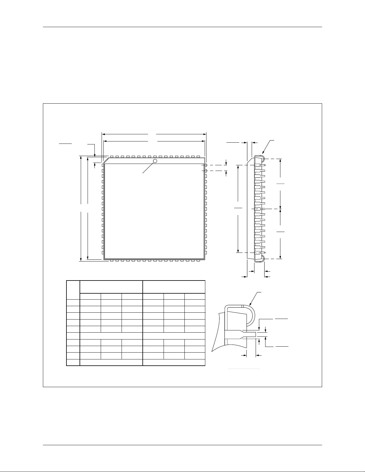
4.0 Mechanical/Electrical Specifications CN8330
4.4 Mechanical Specifications DS3/E3 Framer with 52 Mbps HDLC Controller
4.4 Mechanical Specifications
Figure 4-3. 68–Pin Plastic Leaded Chip Carrier (J-Bend)
68 PLCC
.042"
.048"
S
Y
M
B
O
L
X 45˚
A
A
1
D
1
D
D
2
D
3
E
1
E
E
2
E
3
EE
MIN.
.165
.090
.985
.950
.445
.985
.950
.445
D
D
1
PIN 1 IDENTIFIER
1
INCHES MILLIMETERS
NOM. NOM.
.800 REF. 20.32 REF.
.800 REF. 20.32 REF.
MAX.
.200
.130
.995
.958
.465
.995
.958
.465
MIN.
4.20
2.29
25.02
24.13
11.30
25.02
24.13
11.30
MAX.
5.08
3.30
25.27
24.33
11.81
25.27
24.33
11.81
.042"
.056"
.050" BSC.
.020" MIN.
DETAIL "A"
SEE DETAIL 'A'
D
2
E
2
D
3
E
3
D
2
E
2
1
A
A
.025"/.045" R
.026"
.032"
.013"
.021"
4-8 Conexant 100441E
Page 83
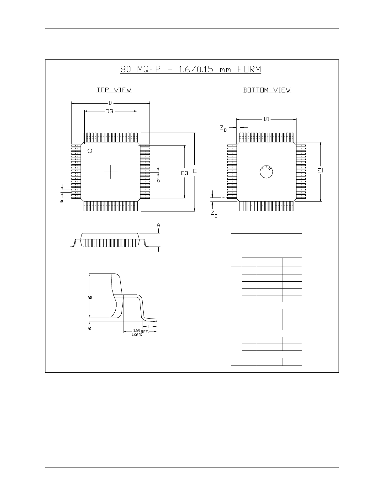
CN8330 4.0 Mechanical/Electrical Specifications
DS3/E3 Framer with 52 Mbps HDLC Controller
Figure 4-4. 80-Pin Metric Quad Flat Pack (MQFP)
4.4 Mechanical Specific a tio ns
S
Y
ALL DIMENSIONS IN
M
B
O
L
A
A1
A2
D
D1
D3
ZD
E
E1
E3
ZE
L
e
b
MILLIMETERS
MIN. NOM. MAX.
----
----
----
.70
----
2.25
0.25
2.0
17.20
14.00
12.35
0.825
17.20
14.00
12.35
0.825
.80
.65
.33
2.20
1.95
17.05
13.95
17.05
13.95
2.30
----
2.05
17.35
14.05
----
17.35
14.05
---.90
----
100441E Conexant 4-9
Page 84

4.0 Mechanical/Electrical Specifications CN8330
4.4 Mechanical Specifications DS3/E3 Framer with 52 Mbps HDLC Controller
4-10 Conexant 100441E
Page 85

A
Appendix A Multimegabit HDLC Formatter
A.1 Introduction
The CN8330 was designed as a DS3/E3 framer with both serial and parallel data
inputs. The circuit has an integral High-Level Data Link Control (HDLC)
interface that can be used without the insertion of DS3/E3 overhead bits. This
mode of operation is documented in this Appendix.
The transmitter is capable of formatting byte-or g anized data from the Payload
Parallel Data Link (PPDL) data port. The parallel data is formatted with idle
flags, zero stuffing for transparency, and a selectable 16- or 32-bit Frame Check
Sequence (FCS) according to ITU-T standard Q.921 or ISO 3309-1984. Options
are provided to allow the formatting of data for packet voice according to ANSI
standard T1.312-1991. Serial data can be transmitted at any rate up to 52 Mbps.
100441E Conexant A-1
Page 86
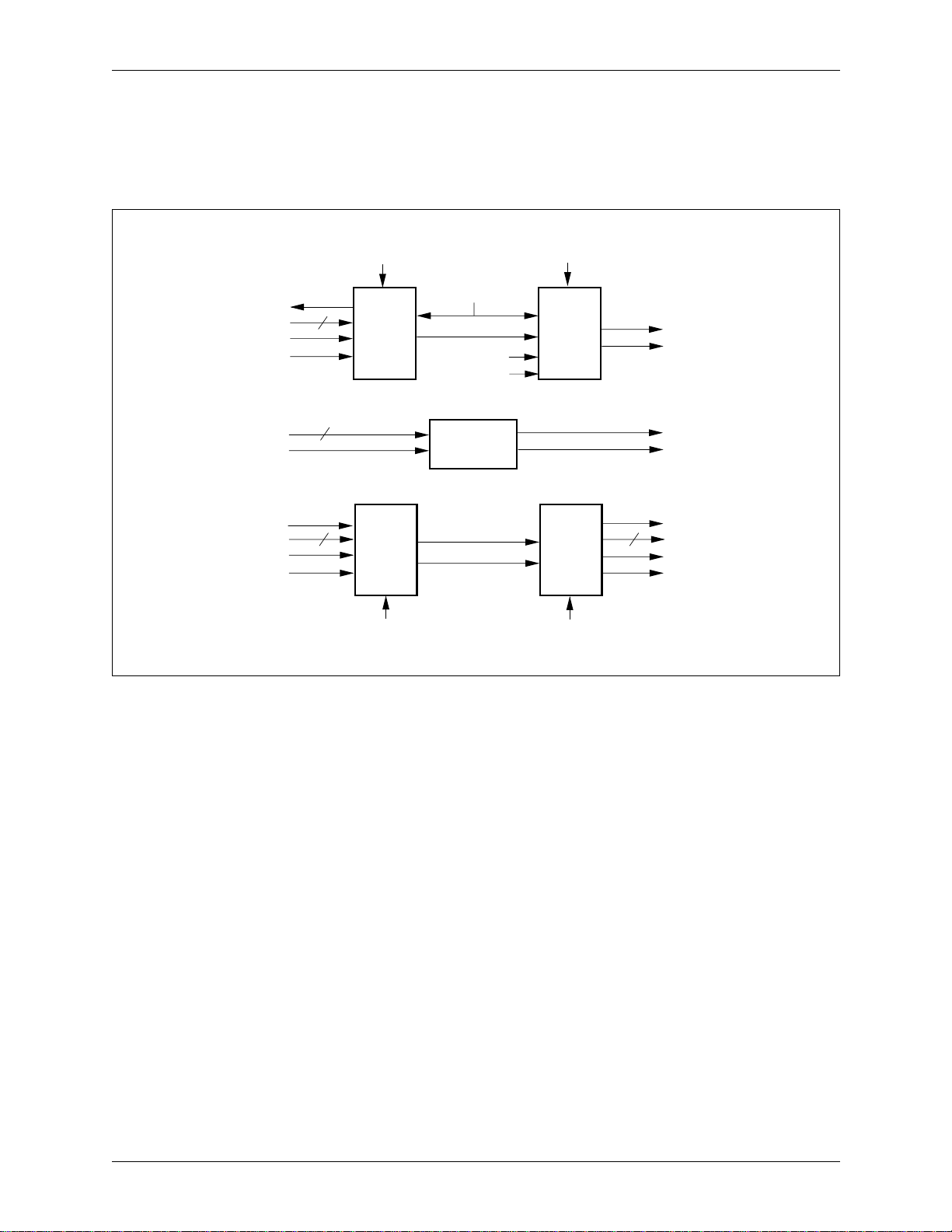
Appendix A Multimegabit HDLC Formatter CN8330
A.1 Introduction DS3/E3 Framer with 52 Mbps HDLC Controller
The receive r provides complementary operation, deriving byte-organized data
and HDLC protocol status including FCS checking at serial rates up to 52 Mbps.
Figure A-1 illustrates the major d a ta paths of the HDLC form atter.
Figure A-1. HDLC Formatter Block Di agram
Transmit Byte Clock
Transmit Data Byte
Send Message
Send FCS
Address/Data
Control
Transmit Data
Transmit Clock
Receive Data
Receive Clock
FCS
Mode
8
8
8 ClockM
HDLC
Transmit
on
off
Source
Loopback
Transmit Clock In
Receive Clock
Receive Data
Microprocessor
Interface
U
X
Data
Data
Line
Loopback
M
off
U
X
on
HDLC
Receive
FCS
Mode
Transmit Clock
Transmit Data
Loopbacks
FCS Mode
Receive Byte Clock
8
Receive Data Byte
Idle Status
FCS Status
A-2 Conexant 100441E
Page 87

CN8330 Appendix A Multimegabit HDLC Formatter
DS3/E3 Framer with 52 Mbps HDLC Controller
A.2 Block and Logic Diagrams
The transmit serial clock is applied to the TXCKI input of the HDLC transmit ter.
The circuit generates a byte clock and eith er idle code, a serialize d message byte,
an FCS sequence, or an abort sequence on the RXCCK/TXNRZ output pin in
response to control signal inputs. At the end of a message, the FCS is generated.
Either a 16- or 32-bit Cycle Redundancy Check (CRC) can be generated for the
FCS. A line loopback function that will loop the receive input directly to the
transmit output for end-to-end loopback is provided.
In the receive direction, serial data is taken from the receiver inputs RXPOS
and RXNEG, or, if source lo opba ck is set, f rom the transmitter output. The serial
clock is connected to the DS3CKI pi n on the HDLC recei ver. The receiver deri ves
bytes of data, a byte clock, idle channel, and valid FCS indications from the
received serial data. The source loopback function can be used to provide a
diagnostic test of the HDLC transmitter and receiver.
A microprocessor interface is required to configure the circuit for HDLC
operation and to control loopbacks and FCS options for the HDLC transmitter
and receiver. The control pins consist of the read and write strobes and a chip
select signal.
A.2 Block and Logic Diagrams
100441E Conexant A-3
Page 88
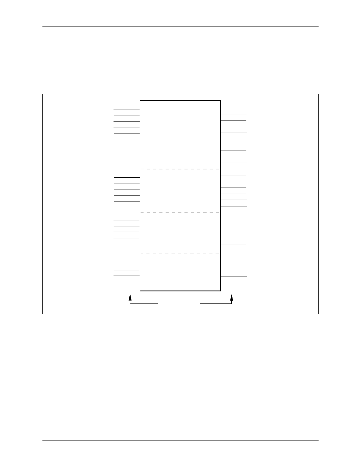
Appendix A Multimegabit HDLC Formatter CN8330
A.2 Block and Logic Diagrams DS3/E3 Framer with 52 Mbps HDLC Controller
Figure A-2 is a logic diagram showing the functional partitioning of the pins.
This diagram pertains only to HDLC mode operation , fo r which some of the pins
are reassigned from CN8330 framer functions, i.e., the transmit data output
comes from a pin (RXCCK/TXNRZ) assigned to the receiver in CN8330 framer
operation.
Figure A-2. HDLC Formatter Logic Diagram
Receive Data Input
Receive Data Input
Receive Clock Input
Ground
Ground
Transmit Clock Input
Ground
Transmit Byte Input
Send FCS Control
Send Message Control
Address Latch Enable
Chip Select
Read Strobe
Write Strobe
Address-Data Bus
Initialization Input
I/O
VCC
Ground
Ground
I
I
I
I
I
I
I
47–50, 53–56
I
I
I
I
I
I
I
I
I
I
I
13
RXPOS
14
RXNEG
15
DS3CKI
16
RXCKI
11
FIFEN
58
TXCKI
45
CBITI
TDAT[7:0]
43
SNDFCS
42
SNDMSG
67
ALE
64
CS
65
RD*
66
WR*
2–9
AD[7:0]
44
PPDLONLY
61
MON/MIC*
60
TESTI
19
INIT*
Receiver
Section
Transmitter
Section
Local Processor
Interface
Control and
Test
RXDAT
RXMSY
RXCLK
CBITO
TXNRZ
RDAT[7:0]
IDLE
VALFCS
VCO
RXBCK
TXBCK
TXCCK
TXPOS
TXNEG
TXSYO
TCLKO
CNTINT
DLINT
TESTO
20
21
22
37
38
34-22
24
25
12
23
57
46
40
39
59
18
62
63
41
Receive Serial Data Output
O
No Connect
O
Receive Clock Output
O
No Connect
O
Transmit Data Output
O
Receive Byte Output
O
Receive Idle Status
O
Receive FCS Status
O
No Connect
O
Receive Byte Clock
O
Transmit Byte Clock
O
No Connect
O
No Connect
O
No Connect
O
No Connect
O
Transmit Clock Output
O
O
No Connect
O
No Connect
O
No Connect
I = Input, O = Output
A-4 Conexant 100441E
Page 89
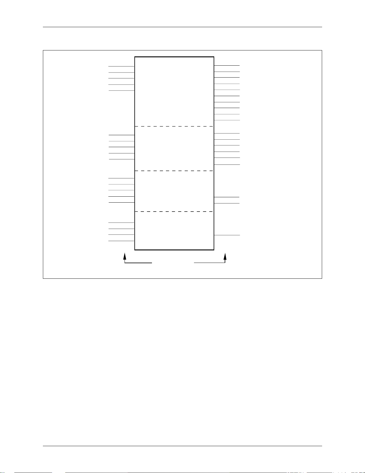
CN8330 Appendix A Multimegabit HDLC Formatter
DS3/E3 Framer with 52 Mbps HDLC Controller
Figure A-3. HDLC Formatter Logic Diagram - 80-Pin MQFP
5
6
7
8
3
56
42
39
38
69
66
67
68
73-80
RXPOS
RXNEG
DS3CKI
RXCKI
FIFEN
TXCKI
CBITI
TDAT[7:0]
SNDFCS
SNDMSG
ALE
CS
RD*
WR*
AD[7:0]
Receiver
Section
Transmitter
Section
Local Processor
Interface
Ground
Ground
Ground
I
I
I
I
I
I
I
I
I
I
I
I
I
I
I/O
Receive Data Input
Receive Data Input
Receive Clock Input
Transmit Clock Input
Transmit Byte Input
Send FCS Control
Send Message Control
Address Latch Enable
Chip Select
Read Strobe
Write Strobe
Address-Data Bus
44-47, 51-54
RXDAT
RXMSY
RXCLK
CBITO
TXNRZ
RDAT[7:0]
IDLE
VALFCS
VCO
RXBCK
TXBCK
TXCCK
TXPOS
TXNEG
TXSYO
TCLKO
CNTINT
DLINT
12
13
14
33
34
22-29
16
17
4
15
55
43
36
35
57
10
64
65
A.2 Block and Logic Diagrams
Receive Serial Data Output
O
No Connect
O
Receive Clock Output
O
No Connect
O
Transmit Data Output
O
Receive Byte Output
O
Receive Idle Status
O
Receive FCS Status
O
No Connect
O
Receive Byte Clock
O
Transmit Byte Clock
O
No Connect
O
No Connect
O
No Connect
O
No Connect
O
Transmit Clock Output
O
O
No Connect
O
No Connect
VCC
Ground
Ground
Initialization Input
41
I
I
I
I
PPDLONLY
63
MON/MIC*
58
TESTI
11
INIT*
Control and
Test
I = Input, O = Output
TESTO
37
O
No Connect
100441E Conexant A-5
Page 90
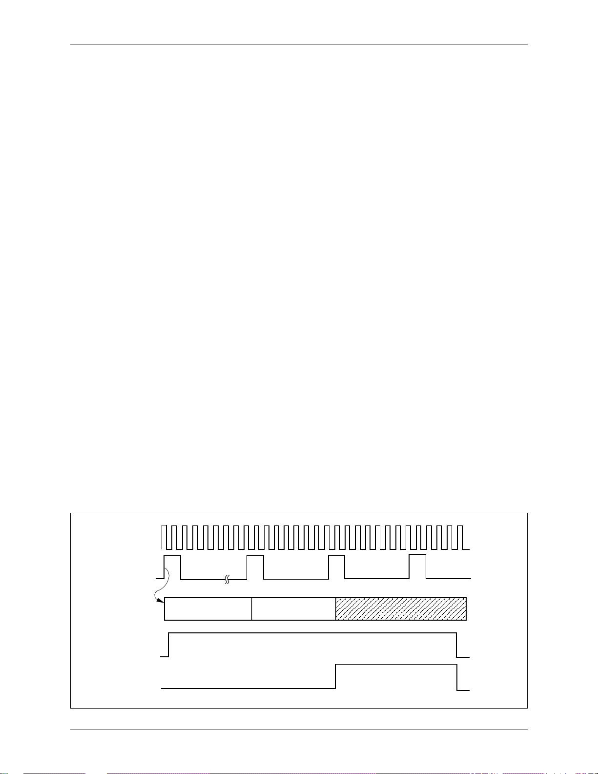
Appendix A Multimegabit HDLC Formatter CN8330
A.3 PPDL Transmitter DS3/E3 Framer with 52 Mbps HDLC Controller
A.3 PPDL Transmitter
The PPDL transmitter is enabled by setting the Parallel Data Enable bit [ParaEn;
CR04.3] in the Feature Control Register [CR04;0x04]. The PPDL formatter is
controlled by signals applied on the SNDMSG and SNDFCS pins. Byte-wide
data is provided on the TDAT[7:0]. Optional HDLC formatting with 16-bit or
32-bit FCSs are provided.
Transmitter operation is controlled by the SNDMSG and SNDFCS pins. If no
message is in pro gress (SNDMSG and SNDFCS both low), idle flags (01111110)
are continuously transmitted in the data stream. Setting SNDMSG high initiates
message transmission. Data bytes and control signals are provided in response to
the rising edge of the transmit byte clock TXBCK and are sampled internally after
the falling edge. The data and controls should be held for a full period of
TXBCK. The least significant bit of the transmitted bytes is applied to TDAT[0]
and the most significant to TDAT[7]; transmission is least significant bit first.
The transmitter performs automatic zero stuffing for transparency and FCS
calculation for the data. The message must be an integral number of bytes in
length. The FCS is 16 or 32 bits in length depending on the setting of the 32-bit
CRC Select control bit [CRC32;CR05.2] in the PPDL Control Register
[CR05;0x05]. If this bit is low, the FCS is calculated with the polynomial:
16+x12+x5
x
SNDFCS shown in Figure A-4 must be high for 4 cycles of the transmit byte
clock and the FCS is calculated with the polynomial:
+1. If a 32-bit CRC is selected by setting the CRC32 high, then
after the last data byte has been transmitted. SNDFCS should be high for 2 byte
clocks in 16-bit FCS mode and for 4 byte clocks in 32-bit FCS mode. An abort
sequence may be transmitte d by setting SNDFCS high w hile SNDMSG is set lo w.
Timing for the transmit operation is shown in Figure A-4.
Figure A-4. PPDL Transmitter Timing
TXCKI
TXBCK
TDAT[7:0]
SNDMSG
SNDFCS
32+x26+x23+x22+x16+x12+x11+x10+x8+x7+x5+x4+x2
x
+x+1
The FCS is transmitted by setting both the SNDMSG and SN DFCS pins high
Data
Data
A-6 Conexant 100441E
Page 91

CN8330 Appendix A Multimegabit HDLC Formatter
DS3/E3 Framer with 52 Mbps HDLC Controller
The transmit byte clock (TXBCK) is g enerated from the transmit c lock input
(TXCKI) and has a duty cycle of 25 percent. TXBCK will nominally be
one-eighth of the TXCKI frequency but is influenced by HDLC transparency bit
insertions. In the absence of any transparency bit insertions, there will be one
pulse on TXBCK for every eight clock cycles of the TXCKI input. When a
transparency bit is inserted into th e serial transmit data stream, the TXBCK
period will be lengthened to nine clock cycles of TXCKI (or 10 clock cycles if
two transparency bit insertions occur within the same octet interval). TXBCK is
present continuously even during the transmission of idle flags. The actual setup
times on TDAT[7:0], SNDMSG, and SNDFCS relative to the rising edge of
TXBCK are negative. Therefore, it is possible to read data and control from a
RAM or FIFO buffer with the rising edge. CN8330 will sample the data after the
falling edge. This allows FIFOs or RAMs with access ti m es of 35–40 ns to be
used.
FCS calculation can be limited to the first N bytes of the transmitted message
by setting the Limit Frame Check Sequence Calculation [LimitFCS;cr05.3]
control bit. In this mode, the FCS is calculated on t he first N bytes transmitted
after the opening flag and then held until the e nd of the message. It is then
appended to the end of the messag e in normal fashion. T he desired number N can
be from 1 to 16 (a value of 0 gives N = 16) and is loaded in the Frame Check
Sequence Calculation Count[3:0] [FCSCnt;CR05.7:4] control f ield. This allows
FCS calculation only on the header information in a T1 packet voice format.
A.3 PPDL Transmitter
A.3.1 PPDL Receiver
The PPDL receiver circuitry is activated when the ParaEn bit in the Feature
Control Register is set. The receiver performs idle flag detection, stuffed zero
deletion, and FCS checking on the incoming data stream. The recovered data
bytes are presented on RDAT[7:0] and are valid on both the rising and falling
edges of RXBCK; the least sign ificant bit is on RDAT[0] and the most signi ficant
bit is on RDAT[7]; the least significant bit is the first received from the serial
input. If the payload stream contains idle flags, the IDLE pin will b e hi gh an d t he
flags will be present on RDAT[7:0]. If a valid FCS is received at the end of the
message block, then the VALFCS pin will be active high while IDLE is high. At
the start of the next message, both indications will go low until the end of the
incoming message has been receiv ed. If a bad FCS is received, IDLE will go high
and VALFCS will remain low. If VALFCS goes high and IDLE does not, an abort
sequence was received in the data. If there is only one flag received between
incoming packets, there will be only one RXBCK pulse present while IDLE is
high. If CRC 32-bit is low, the FCS is checked with the polynomial:
16+x12+x5
x
+1
If a 32-bit CRC is selected b y setting CRC32 bit hig h, then the FCS is check ed
with the polynomial:
32+x26+x23+x22+x16+x12+x11+x10+x8+x7+x5+x4+x2
x
+x+1
100441E Conexant A-7
Page 92

Appendix A Multimegabit HDLC Formatter CN8330
A.3 PPDL Transmitter DS3/E3 Framer with 52 Mbps HDLC Controller
Timing for this operation is shown in Figure A-5. Shown are cases of a good
packet received, a packet received with a bad FCS, and an aborted packet. Each
packet is shown with one idle flag marking the end of the packet and the start of
the next packet. However, more than one flag can occur in the serial stream. The
output data will contain each occurrence of idle or abort flags with a pulse on
RXBCK.
The receive byte clock RXBCK is generated from the falling edge of the
receive serial clock input on DS3CKI and is present continuousl y like the transmit
byte clock. Nominally there will be one pulse on RXBCK for every eight clock
cycles on the receive serial clock. When an inserted transparency bit must be
deleted , th e RXBCK period will be l engthened b y one seri al clock c ycle. RXBCK
is present during the reception of FCS octets and idle flags. On a received
message with a valid 16-bit FCS, the la st 2 byte clocks prior to IDLE and
VALFCS going high will be the received FCS octets that were appended to the
end of the message by the transmitter. In 32-bit mode, the last four received octets
will be FCS octets. The R D AT[7:0], IDLE, and VALFCS outputs are valid at least
one serial clock cy cle period before the rising ed ge of RXB CK and are v ali d for at
least two serial clock cycle periods after the falling edge of RXBCK.
FCS checking can be limited to the first N bytes of the received message by
setting the LimitFCS control bit. In this mode, the FCS is checked only on the
first N bytes received after the opening flag and then held until the end of the
message. The locally calculated FCS is then compared to the last 2/4 bytes in the
message to determine if a valid FCS was received. The desired number N can be
from 1 to 16 (a value of 0 gives N=16) and is loaded in the FCSCnt control field.
This allows FCS checking only on the header information in a T1 packet vo i ce
format.
A-8 Conexant 100441E
Page 93
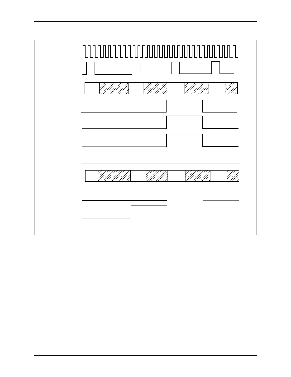
CN8330 Appendix A Multimegabit HDLC Formatter
DS3/E3 Framer with 52 Mbps HDLC Controller
Figure A-5. PPDL Receiver Timing
RXCLK
RXBCK
RDAT[7:0]
IDLE
Good Packet
VALFCS
IDLE
Packet w/Bad FCS
VALFCS
Data
FCS
Data
FCS
Flag
A.3 PPDL Transmitter
Data
RDAT[7:0]
IDLE
Aborted Packet
VALFCS
Data
Abort
Flag
Data
100441E Conexant A-9
Page 94
Appendix A Multimegabit HDLC Formatter CN8330
Control Registers DS3/E3 Framer with 52 Mbps HDLC Controller
Control Registers
0x00—Mode Control Register (CR00)
NOTE: Rsvd bits in Control Registers must be set to zero.
7 6 5 4 3 2 1 0
LineLp SourceLP Rsvd Rsvd Rsvd Rsvd Rsvd Rsvd
LineLp Line Loopback Enable—Set to enable the loopback in the external direction. This loopback
connects the recei v ed data stream before B3ZS/HDB3 decoding to the transmitter outpu ts. T he
received data is still presented to all receiver blocks and is present on the receiver output pins.
SourceLp Source Loopback Enable—Set to enable the loopback in the internal direction. This loopback
connects the encoded transmitter data and clock directly to the receiver. Transmission of data
on the line is not affected by this loopback.
0x04—Feature Control Register (CR04)
The Feature Control Register is provided to enable or disable miscellaneous features in the CN8330 Framer.
NOTE: Rsvd bits in Control Registers must be set to zero.
7 6 5 4 3 2 1 0
Rsvd Rsvd Rsvd Rsvd ParaEn Rsvd Rsvd Rsvd
ParaEn Parallel Data Enable—Set high to enable the PPDL transmitter and receiver as the source and
sink for data. Eight-bit data bytes are provided on the TDAT[7:0] and RDAT[7:0] buses for the
PPDL transmitter and receiver. This bit must be set to 1 for operation as an HDLC formatter.
A-10 Conexant 100441E
Page 95

CN8330 Appendix A Multimegabit HDLC Formatter
DS3/E3 Framer with 52 Mbps HDLC Controller
Control Registers
0x05—PPDL Control Register (CRO5)
The PPDL Control Register is provided to control the mode of operation of the PPDL transmitter and receiver.
NOTE: Rsvd bits in Control Registers must be set to zero.
7 6 5 4 3 2 1 0
FCSCnt[3] FCSCnt[2] FCSCnt[1] FCSCnt[0] LimitFCS CRC32 Rsvd Rsvd
FCSCnt[3:0] FCS Calculation Count—Determines the number of bytes over which the FCS is to be calcu-
lated. The number of bytes for calculation can be from 1 to 16 (a value of zero defaults to 16
bytes of calculation).
LimitFCS Li mit FCS Calcula tion—Set to enable FCS c alculation only on the first N bytes of an HDL C
frame where N is determined by the FCS calculate count field. If this bit is low, the FCS will
be calculated over all transmitted bytes.
CRC32 32-Bit CRC Select—Set high to enable 32-bit CRC generation and checking on the PPDL. If
this bit is low, then 16 -bit CRC generation and c he c king is enabled.
100441E Conexant A-11
Page 96

Appendix A Multimegabit HDLC Formatter CN8330
Control Registers DS3/E3 Framer with 52 Mbps HDLC Controller
A-12 Conexant 100441E
Page 97

B
Appendix B
This appendix describes the various non-conformances associated with this
device.
B.1 DS3CKI Clock Duty Cycle
Conexant recommends a 60/40 percent duty cycle maximum for the DS3CKI
input.
B.2 Overhead Bit Insertion in E3 Parallel Payload Mode
When the framer is operated in E3 Parallel Payload mode with external overhead
insertion enabled, the receive byte clock does not provide pulses where the
overhead bits are inserted.
Workaround: An external hardware circuit can be constructed to provide a
continuous byte clock synchronous to the receive byte clock. Contact the
Conexant applications department for circuit details.
100441E Conexant B-1
Page 98

Appendix B CN8330
B.3 HDLC Formatter Mode Support While Configured for E3 Framing DS3/E3 Framer with 52 Mbps HDLC Controller
B.3 HDLC Formatter Mode Support While Configured for E3 Framing
This mode was previously selected by configuring the following bits: CR00.3=1
(E3Frm), CR04.3 (ParaEn) and CR05.1=0 (DisPPDL).If this mode is selected, the
zero insertion function of the HDLC formatter incorrectly inserts an extra zero
when the transmitted HDLC packet contains stuffed zeros that overlap the 16-bit
E3 overhead. This transmitter malfunction causes the HDLC receiver to interpret
the extra zero as data which results in an FCS errored packet. This problem
prevents any customer from developing an E3 framed HDLC mode application.
Notice that parallel data still functions properly in E3 mode if CR05.1=1
(DisPPDL).
Workaround: By using two CN8330 devices with one operating in HDLC
formatter mode and another device exclusively in E3 mode same results can be
achieved.
B-2 Conexant 100441E
Page 99
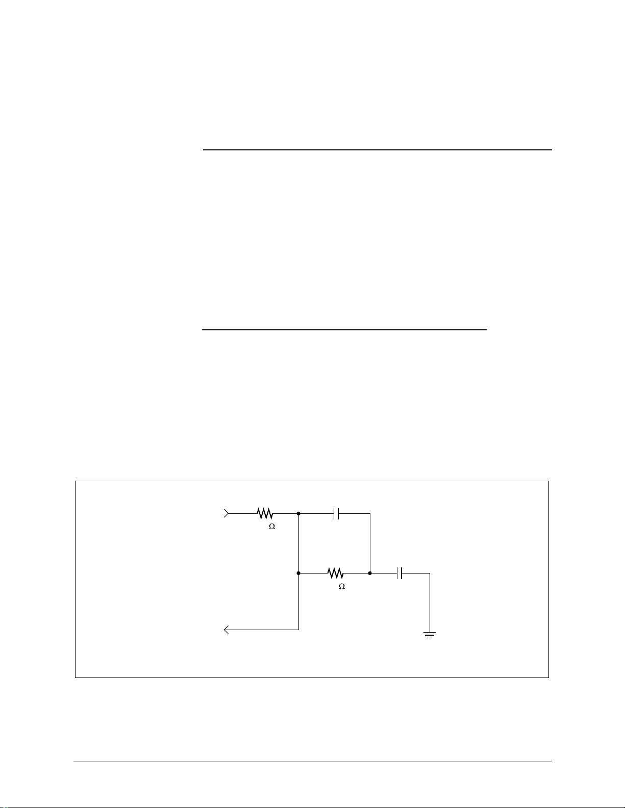
C
Appendix C
Here's what w e'v e recommended as a st arting point for those customers who need
a jitter attenuatio n PLL for TBR24 comp liance in E3 mode.
An external jitter attenuation PLL can be implemented for CN8330 with one
VCXO and a passive LPF (low pass filter). The VCO output from CN8330 is
passed through the LPF to create a control voltage input to the VCXO. The
VCXO output then connects to RXCKI (and optionally to TXCKI) input of
CN8330.
VCXO Specifications: T3 E3 Units
Center Frequency: 44.736 34.368 MHz
Frequency Accuracy: +/- 20 +/- 20 ppm
Frequency Pullability: +/- 200 +/- 200 ppm
Note: +/- 100 ppm frequency pullability may be adequate.
The LPF circuit is shown below with the RC time constants used to establish
the filter's cutoff frequencies as follows:
T1 = R1 x C2
T2 = R2 x C2
T3 = R2 x C1
From VCO
Output
To VCXO
Control
Input
R1 C1
1 M
10 nF
R2 C2
1 M
100 nF
GND
(Analog)
R and C values shown above are calculated for typical applications.
8330_001
100441E Conexant C-1
Page 100

Appendix C CN8330
DS3/E3 Framer with 52 Mbps HDLC Controller
The overall jitter transfer function also depends on the VCXO control
voltage/frequency conversion ratio (Ko) parameter measured in radians per
second per volt. In our PLL loop filter calculations, Ko equals approximately
400 for a VCXO with +/- 200 ppm pullability. Given Ko , a 10Hz brea k frequenc y
is calculated for R1=R2=500K. With a 10Hz break, attenuation at 100Hz is
around -12dB, barely sufficient to meet 0.4UI output jitter required with 1.5UI
input and 0.08UI intrinsic jitter.
For added margin, R1=R2=1M puts the break frequency at 7Hz.
Several CN8330 customers have tested the jitter attenuation PLL with
successfull results using R1=R2=1M. While this LPF should work for both T3
and E3 applications, we have not tested the PLL to comply with any regulatory or
interface requirements. LPF cutoff frequencies might have to be scaled to match
desired loop timing characteristics or to have the desired cutoff frequency. We
recommend all customers conduct performance evaluation and characterization
testing of the PLL before sending equipment for certification.
C-2 Conexant 100441E
 Loading...