

CALIFORNIA MICRO DEVICES
n
r
ubes
m
USB Peripheral Power Management
CMPWR160
Features
• 3.3V regulated output up to 500mA
• Quiescent current 35µA (typical)
• Shutdown mode current 7µA (typical)
• 30ms active LOW Power-On Reset (POR) pulse
• Thermal overload protection
• Foldback current limiting protection
• Reverse-current protection
• 8 pin SOIC power package
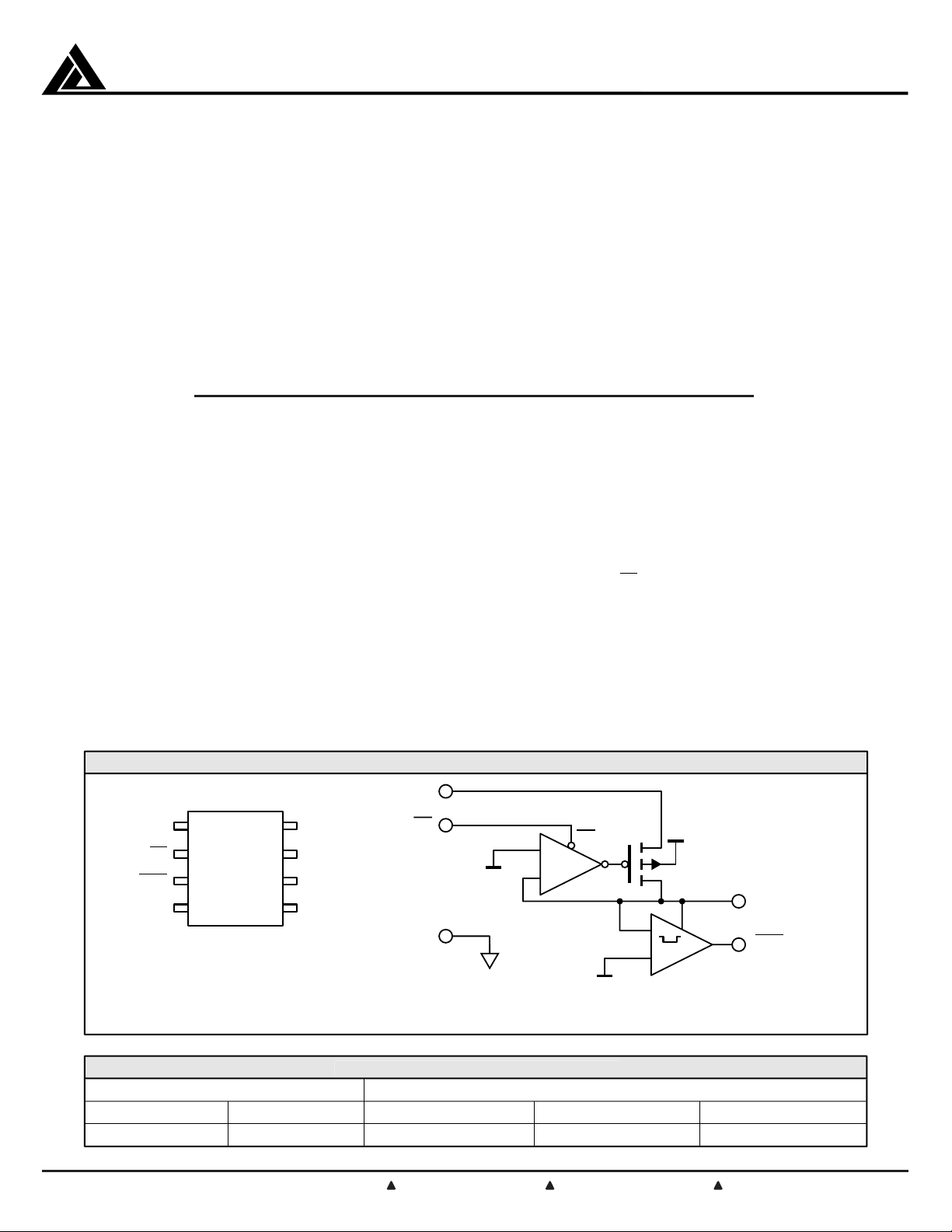
The SmartORTM CMPWR160 combines a Low Dropout
Regulator (LDO) with a Power-On Reset (POR) pulse
generator, and is intended for Universal Serial Bus
(USB) peripherals. To meet the specification requirements of both USB 1.0 and USB 2.0, the CMPWR160
draws a very low quiescent current (35µA), and delivers
up to 500mA of load current at a fixed 3.3V output.
The POR pulse (active LOW) has a typical duration of
30ms after the output has exceeded and stabilized
above 2.9V. Thus a new POR pulse is developed each
time the regulator power is interrupted and restored,
which occurs often on USB buses when cables are
connected (or disconnected) by the user. It is not
necessary to have a VCC supply for POR to operate,
allowing the CMPWR160 to work in Wired-ORed power
systems.
Applications
• Bus-powered USB peripherals
• Self-powered USB peripherals
• Portable/battery-powered devices
• Critical power monitoring, hot-insertion devices
When VCC is powered down, the device will automatically
enter reverse-current protection mode and maintain
isolation between V
tions that can use power from the USB port in addition to
internal batteries or an AC adapter supply (Wired-ORed
power systems). In the event of V
, the device will automatically enter shutdown mode
V
OUT
and fully isolate the V
A ShutDown input (
powered down on demand. While in shutdown mode the
POR circuitry will remain active, making the device
suitable for systems which contain backup or alternative
power sources.
The CMPWR160 is available in an 8-pin SOIC thermally
enhanced package, ideal for applications where space
is tight.
and VCC. This is useful for applica-
OUT
collapsing below
CC
power source from the output.
CC
SD
) forces the regulator to be
Block Diagra
V
CC
SD
V
GND
V
SD
POR
V
OUT
CC
Top View
1
2
3
4
CMPWR160
8 LEAD SOIC
8
GND
7
GND
6
GND
5
GND
Pin Diagram
Standard Part Ordering Informatio
Package Ordering Part Numbe
8 Power SOIC CMPWR160SA/T CMPWR160SA/R CMPWR160SA
©2000 California Micro Devices Corp. All rights reserved. SmartOR™ is a trademark of California Micro Devices Corporation.
12/5/2000
215 Topaz Street, Milpitas, California 95035 Tel: (408) 263-3214 Fax: (408) 263-7846 www.calmicro.com
Style T
SD
+
REF
3.3V
–
+
30ms
–
2.9V
Simplified Electrical Schematic
Tape & Reel Part Marking
V
OUT
3.3V/500mA
POR
C1571000
1
CALIFORNIA MICRO DEVICES
s
t
5.5
gs
g
t
)
000
s
)
T
I
500
35.30.465
Absolute Maximum Ratin
Parameter Ratin
ESD Protection (HBM
VCC/V
Voltage 6.0, GND –0.5 V
OUT
SD Logic Input Voltage V
POR Logic Output Voltage V
OUT
2
+ 0.5, GND –0.5 V
CC
+ 0.5, GND –0.5
Temperature: Storage –40 to 150
Power Dissipation
Operating Ambient 0 to 70
Operating Junction 0 to 125
Note 1
Internally Limited
Operating Condition
Parameter Range
4.2 to
Temperature (Ambient) 0 to 70
Load Current 0 to 500 mA
10 ± 10% µF
C
EXT
ni
V
˚
ni
C
˚
CMPWR160
C
Electrical Operating Characteristic
(over operating conditions unless specified otherwise
Symbol Parameter
Regulator Output Voltage
OUT
I
Regulator Current Limit 550 mA
LIM
I
S/C
V
R LOAD
V
R LINE
Regulator Dropout Voltage MIN VCC – V
V
DO
Quiescent Supply Current Regulator Enabled (No Load) 35 50 µA
I
Q
Shutdown Supply Current Regulator Disabled 7 10 µA
I
SD
VCC Pin Reverse Leakage V
I
RCC
V
IH SD
V
IL SD
V
POR
T
POR
R
POR
Short-Circuit Current Limit 300 mA
Load Regulation VCC = 5V, I
Line Regulation VCC = 4.2V to 5.5V, I
Shutdown High Detect VCC = 5V 3.0 V
Shutdown Low Detect VCC = 5V 1.0 V
POR Detect Threshold 4.2V < VCC < 5.5V 2.8 2.9 3.0 V
POR Pulse Duration 20 30 40 ms
POR Output Impedance After POR Threshold Detected 0.2 0.5 2 kΩ
T
T
Note 1: The SOIC package used is thermally enhanced through the use of a fused integral leadframe. The power rating is based on a printed
Shutdown Temperature 160
DISABLE
Thermal Hysteresis 20
HYST
circuit board heat spreading capability equivalent to 2 square inches of copper connected to the GND pins. Typical multi-layer boards
using power plane construction will provide this heat spreading ability without the need for additional dedicated copper area. (Please
consult with factory for thermal evaluation assistance.)
mA <
OUT
Sinking to GND/Sourcing from V
onditions
<
LOAD
LOAD
OUT
mA
= 5mA to 500mA 75 mV
= 5mA 2 mV
LOAD
for I
= 500mA 0.6 0.9 V
LOAD
.1
NI
= 3.3V, VCC = 0V 1 10 µA
CC
˚
˚
C
C
©2000 California Micro Devices Corp. All rights reserved. SmartOR™ is a trademark of California Micro Devices Corporation.
215 Topaz Street, Milpitas, California 95035 Tel: (408) 263-3214 Fax: (408) 263-7846 www.calmicro.com
2
12/5/2000
CALIFORNIA MICRO DEVICES
s
n
V
.
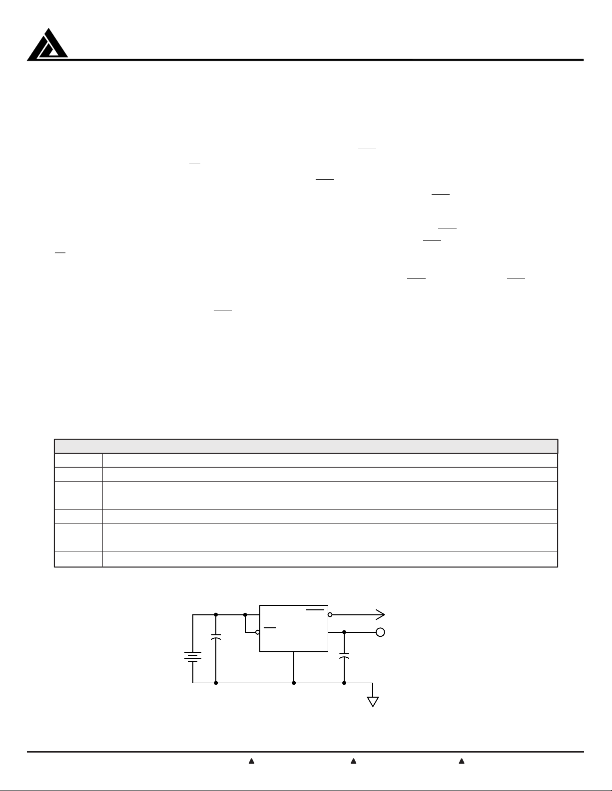
Interface Signals
CMPWR160
VCC is the input power source for the Low Drop Out
Regulator, capable of delivering 3.3V/500mA output
current even when the input is as low as 4.2V.
Internal loading on this pin is typically 35µA when the
regulator is enabled, which reduces to only 7µA when-
SD
ever the regulator is shutdown (
event of V
collapsing below V
CC
taken Low). In the
, the loading at VCC will
OUT
immediately reduce to less than 0.1µA.
If the V
pin is within a few inches of the main input
CC
filter, a capacitor may not be necessary. Otherwise an
input filter capacitor in the range of 1µF to 10µF will
ensure adequate filtering.
is the regulator shutdown input logic signal which is
SD
Active Low. This is a true CMOS input signal referenced
to V
supply. When the pin is tied High (VCC ) the
CC
regulator operates fully. When the pin is taken to GND,
the device enters shutdown mode and the regulator is
fully disabled. In this mode all critical
POR
circuitry
remains fully powered consuming less than 7µA (typical).
V
is the regulator output voltage used to power the
OUT
load. An output capacitor of 10µF is used to provide the
necessary phase compensation, thereby preventing
oscillation. The capacitor also helps to minimize the peak
output disturbance during line or load transients. Whenever V
collapses below the output the device immedi-
CC
ately enters reverse protection mode to prevent any
current flow back into the regulator pass transistor.
Under these conditions V
will also be used to provide
OUT
the necessary quiescent current for the internal reference and
POR
circuits. This ensures excellent start-up
characteristics for the regulator.
POR
is the Power-On-Reset output pin (Active Low).
When V
rises above the
OUT
POR
threshold voltage
(typically 2.9V), the pin is forced to logic low (GND). The
pin remains logic low for 30ms then it is forced logic high
(3.3V). If V
falls below the
OUT
during this 30ms interval
POR
threshold voltage
POR
will remain logic low. If it
falls below the voltage threshold and then recovers the
30ms time will reset.
If V
falls below the
OUT
POR
threshold voltage
POR
is
immediately forced to logic low.
The power-on reset circuitry is designed to remain active
under all conditions and will produce a valid output even
when V
is not present. A very low quiescent current
CC
(7µA typical) ensures continuous operation of the POR
circuit.
GND is the negative reference for all voltages. This
current that flows in the ground connection is very low
(35µA typical with the regulator enabled and 7µA typical
with the regulator disabled).
Pin Function
Symbol Descriptio
Positive supply input for regulator. When V falls below
the regulator is disabled
T
SD Shutdown control input signal (Active Low) to disable internal voltage regulator and current supply
to less than 7µA.
POR Power-On-Reset output signal is held Low until the output has been stable (>2.9V) for at least 30ms.
V
Regulator voltage ouput (3.3V) capable of delivering 500mA when device is enabled (SD is High).
OUT
Whenever the output exceeds 2.9V (TYP) the POR pulse is triggered.
GND Negative reference for all voltages
CMPWR160
V
CC
C
+
V
CC
5V
+
–
IN
1µF
SD
GND
POR
V
OUT
+
C
OUT
10µF
uP Reset
V
OUT
3.3V/500mA
GND
Typical Application Circuit
©2000 California Micro Devices Corp. All rights reserved. SmartOR™ is a trademark of California Micro Devices Corporation.
12/5/2000
215 Topaz Street, Milpitas, California 95035 Tel: (408) 263-3214 Fax: (408) 263-7846 www.calmicro.com
3

CALIFORNIA MICRO DEVICES
Typical DC Characteristics
Unless stated otherwise, all DC characteristics were
measured at room temperature with a nominal V
supply voltage of 5V and an output capacitance of 10µF.
Resistive load conditions were used.
Line Regulation Characteristics of the regulator are
shown in Figure 1. At maximum rated load conditions
(500mA), a 100mV drop in regulation occurs when the
line voltage has collapses below 3.8V. For light load
conditions (5mA), regulation is maintained for line
voltages as low as 3.3V.
CC
3.35
3.30
3.25
3.20
(V)
OUT
3.15
V
3.10
3.05
3.0 3.5 4.0
Figure 1. Line Regulation
5mA Load
VCC (V)
CMPWR160
500mA Load
4.5
5.0
Load Regulation performance is shown from zero to
maximum rated load in Figure 2. A 10% to 100% change
of rated load, results in an output voltage change of less
than 10mV. This translates into an effective output
impedance of approximately 0.02Ω.
Ground Current is shown across the entire range of
load conditions in Figure 3. The ground current increases
by 40µA across the range of load conditions. This
increase is due to the current limiting protective circuitry
becoming active.
(V)
OUT
V
3.40
3.35
3.30
3.25
3.20
0 200 400
Load Current (mA)
Figure 2. Load Regulation
100
80
60
40
600
Ground Current (µA)
20
©2000 California Micro Devices Corp. All rights reserved. SmartOR™ is a trademark of California Micro Devices Corporation.
215 Topaz Street, Milpitas, California 95035 Tel: (408) 263-3214 Fax: (408) 263-7846 www.calmicro.com
4
0
0 200 400
Load Current (mA)
Figure 3. Ground Current
600
12/5/2000

CALIFORNIA MICRO DEVICES
Typical DC Characteristics continued
CMPWR160
VCC Operating Current (no load, SD high) is shown
across a range of V
supply voltages with the regulator
CC
enabled in Figure 4. The graph shows that the operating
current is 35µA typical and changes by less than 1µA
across this range.
VCC Shutdown Current variation with the VCC supply
voltage is shown in Figure 5.
60
50
40
30
20
Supply Current (µA)
10
0
3.5 4.5 5.5
V
(V)
CC
Figure 4. VCC Operating Current (no load)
10
8
6
4
Supply Current (µA)
2
0
1.5 2.5 3.5
(V)
V
CC
Figure 5. VCC Shutdown Current
5.54.5
©2000 California Micro Devices Corp. All rights reserved. SmartOR™ is a trademark of California Micro Devices Corporation.
215 Topaz Street, Milpitas, California 95035 Tel: (408) 263-3214 Fax: (408) 263-7846 www.calmicro.com
12/5/2000
5

CALIFORNIA MICRO DEVICES
Typical Transient Characteristics
CMPWR160
The transient characterization test setup is shown in
Figure 6. It was the setup used for the transient tests
unless specified otherwise.
A maximum rated load current of 6.6Ω (500mA @ 3.3V)
was used during characterization along with a nominal
V
supply voltage of 5V DC, unless specified otherwise.
CC
The load transient characterization was done by switching between 6.6 and 660Ω load resistors. This switched
the load between 500 and 5mA respectively.
For the V
V
supply was ramped between 0 and 5V. Both the rise
CC
and fall times for the V
power-up and power-down characterizations
CC
power-up/down pulses were
CC
controlled to be 15ms.
CMPWR160
V
CC
V
CC
+
C1
10µF
C2
0.1µF
SD
In the line transient characterizations the V
voltage was controlled to step between 4.5 to 5.5V.
For the
tied to ground and the V
response characterization VCC and SD were
POR
voltage was directly driven
OUT
between 2.7 and 3.1V. This was done by connecting a
function generator directly to the output of the device.
These voltage values were picked because it drove V
directly across the typical
V
was tied to ground to show that the
CC
operate even when the V
threshold voltage of 2.9V.
POR
POR
supply voltage is not present.
CC
The oscilloscope traces show the full bandwidth response at the
SD
,
POR
, V
CC
and V
pins depending on
OUT
the characterization.
POR
V
OUT
GND
+
C3
0.1µF
C4
10µF
(500mA)
6.6Ω
supply
CC
circuitry will
POR
V
OUT
OUT
GND
Figure 6. Transient Characterization Test Setup
power-up Cold Start
V
CC
Figure 7 shows the output response during an initial V
power up with SD tied to VCC. When VCC reaches a
particular threshold, the regulator turns on. The uncharged output capacitor causes maximum inrush
current to flow. At this point the device sees the output
as a short circuit and the device enters a protective
current limiting mode. The output capacitor quickly
charges and V
below V
the inrush current stops flowing and the output
CC
rises with the input. V
rises. Once this voltage rises to just
OUT
continues to rise with the input
OUT
until it reaches 3.3V.
GND
CC
Tek Run Sample
25.0kS/s
1.00V
Ch2
V
CC
V
OUT
1.00V
M 2.00ms
(500mA Load)
280mV
Ch2
©2000 California Micro Devices Corp. All rights reserved. SmartOR™ is a trademark of California Micro Devices Corporation.
215 Topaz Street, Milpitas, California 95035 Tel: (408) 263-3214 Fax: (408) 263-7846 www.calmicro.com
6
Figure 7. VCC Power-up Cold Start
12/5/2000

CALIFORNIA MICRO DEVICES
CMPWR160
Typical Transient Characteristics continued
VCC Power down
Figure 8 shows the output response of the regulator
during a complete power down situation under full load
conditions with
Shutdown Transient Response
The transient response of the output voltage to the
pin is shown in Figure 9. The graph shows that a rising
edge on the
edge disables the regulator.
The rise and fall time for the output voltages are 100µs
and 200µs respectively.
SD
tied to VCC.
SD
pin enables the regulator and a falling
SD
Tek Run Sample
25.0kS/s
V
OUT
1.00V
Ch2
V
CC
1.00V
Figure 8. VCC Power Down
Tek 3 Acqs
2
25.0kS/s
SD
M 2.00ms
(500mA Load)
3.50V
Ch2
POR
Response
The transient response of the active low POR pin to V
is shown in Figure 10. When V
POR
threshold voltage (typically 2.9V), the pin is forced
rises above the
OUT
OUT
to logic low (0V). The pin remains at logic low for 30ms
then it is forced to logic high (3.3V). If V
threshold voltage during this 30ms interval
POR
falls below the
OUT
POR
will remain logic low. If it falls below the voltage threshold
and then recovers the 30ms time will reset.
When V
falls below the
OUT
POR
threshold voltage
POR
is
immediately forced to logic low.
V
is tied to ground to show that the
CC
work without V
present.
CC
POR
circuitry will
(500mA Load)
V
OUT
1.00V
Ch2
5.00V
M 200µs
Ch2
Figure 9. Shutdown Transient Response
V
POR
5.0kS/s
3.1V
OUT
2.7V
Tek Run Sample
2
3.0V
©2000 California Micro Devices Corp. All rights reserved. SmartOR™ is a trademark of California Micro Devices Corporation.
215 Topaz Street, Milpitas, California 95035 Tel: (408) 263-3214 Fax: (408) 263-7846 www.calmicro.com
12/5/2000
1.00V
Figure 10.
Ch2
200mV
POR
M 10.0ms
Ch2
Response
2.90V
7

CALIFORNIA MICRO DEVICES
Typical Transient Characteristics continued
Load Step response
Figure 11 shows the output voltage (Ch1) response of
the regulator during a step load change between 5mA
and 500mA (represented on Ch2). For the 5mA to
500mA transition an initial transient overshoot of 60mV
occurs and then the output settles to its final voltage
within 20µs. For the 500mA to 5mA transition there is
also an initial overshoot of 60mV however it takes
approximately 250µs to settle to its final voltage.
The overall DC voltage disturbance on the output is
approximately 25mV, which demonstrates the regulator
output impedance of 50mΩ.
V
offset = 3.3V
OUT
Tek Run Sample
1
250kS/s
500mA
Load
5mA
VOUT (offset = 3.3V)
CMPWR160
Line Step Response
Figure 12 shows the output response of the regulator to
a V
line voltage transient between 4.5V and 5.5V
CC
(1Vpp as shown on Ch2). The load condition during this
test is 5mA. The output response produces less than
10mV of disturbance on both edges indicating a line
rejection of better than 40dB at high frequencies.
V
offset = 3.3V
OUT
Reset response time with overdrive
Figure 13 shows the time it takes for the
reset when the output voltage is driven below the
POR
signal to
POR
trigger threshold by varying amounts. The amount the
voltage is driven below the POR trigger threshold is the
overdrive voltage.
Ch1
50.0mV
2.00V
Figure 11. Load Step Response
V
CC
4.5V
20.0mV
250kS/s
5.5V
(5mA Load)
V
OUT(offset = 3.3V)
M 200µs
500mV
Ch2
Tek 2 Acqs
2
Figure 12. Line Step Response
1000
100
Ch2
Ch2
1.60VM 200µs
5.00V
10
Turn Off Delay (µs)
Figure 13. Reset Response Time with Overdrive
©2000 California Micro Devices Corp. All rights reserved. SmartOR™ is a trademark of California Micro Devices Corporation.
215 Topaz Street, Milpitas, California 95035 Tel: (408) 263-3214 Fax: (408) 263-7846 www.calmicro.com
8
1
0 50 100 150 200
Overdrive (mV)
250 300
12/5/2000

CALIFORNIA MICRO DEVICES
Typical Thermal Characteristics
CMPWR160
Thermal dissipation of junction heat consists primarily of
two paths in series. The first path is the junction to the
case (θJC) thermal resistance which is defined by the
package style, and the second path is the case to
ambient (θ
) thermal resistance, which is dependent on
CA
board layout.
The overall junction to ambient (θ
) thermal resistance is
JA
equal to:
θ
= θJC + θ
JA
CA
For a given package style and board layout, the operating junction temperature is a function of junction power
dissipation P
, and the ambient temperature, resulting
JUNC
in the following thermal equation:
T
= T
JUNC
= T
AMB
AMB
+ P
+ P
JUNC
JUNC
(θ
(θJA)
JC
) + P
JUNC
(θCA )
The CMPWR160SA is housed in a thermally enhanced
package where all the GND pins (5 through 8) are
integral to the leadframe (fused leadframe). When the
device is mounted on a double sided printed circuit
board with two square inches of copper allocated for
“heat spreading”, the resulting θ
is 50°C/W.
JA
Based on a maximum power dissipation of
1.0W (2Vx500mA) with an ambient of 70°C the resulting
junction temperature will be:
T
JUNC
= T
AMB
+ P
JUNC
(θ
)
JA
= 70°C + 1.0W (50°C/W)
= 70°C + 50°C = 120°C
All thermal characteristics of the CMPWR160SA were
measured using a double sided board with two square
inches of copper area connected to the GND pins for
“heat spreading”.
Measurements showing performance up to junction
temperature of 125°C were performed under light load
conditions (5mA). This allows the ambient temperature to
be representative of the internal junction temperature.
Note: The use of multi-layer board construction with
power planes will further enhance the thermal performance of the package. In the event of no copper area
being dedicated for heat spreading, a multi-layer board
construction, using only the minimum size pad layout,
will typically provide the CMPWR160SA with an overall
θ
of 70°C/W which allows up to 780mW to be safely
JA
dissipated.
Output Voltage vs. Temperature
Figure 14 shows the regulator V
performance up to
OUT
the maximum rated junction temperature. A 125°C
variation in junction temperature from –25°C causes an
output voltage variation of about 50mV, reflecting
a voltage temperature coefficient of approximately
±50ppm/°C.
3.35
3.33
3.31
(v)
OUT
V
3.29
3.27
3.25
–25 25075
Figure 14. V
Temperature Variation (5mA)
OUT
50 100 125
Temperature (˚C)
©2000 California Micro Devices Corp. All rights reserved. SmartOR™ is a trademark of California Micro Devices Corporation.
215 Topaz Street, Milpitas, California 95035 Tel: (408) 263-3214 Fax: (408) 263-7846 www.calmicro.com
12/5/2000
9

CALIFORNIA MICRO DEVICES
Typical Thermal Characteristics continued
CMPWR160
Output Voltage (Rated) vs. Temperature
Figure 15 shows the regulator steady state performance
when fully loaded (500mA) from –25°C up to the rated
maximum temperature of 70°C. The output variation at
maximum load is approximately 20mV across the shown
operating temperature. This translates to a temperature
coefficient of approximately ±30ppm/°C.
POR
Voltage Threshold Temperature Variation
Figure 16 shows the
POR
threshold voltage variation
from –25°C up to the maximum rated junction temperature. The overall 150°C change in junction temperature
causes less than a 5mV variation in the
POR
threshold
voltage. This translates to a temperature coefficient of
±6ppm/°C.
The POR pulse duration does not vary with temperature.
3.34
3.32
3.30
(v)
OUT
V
3.28
3.26
3.24
–25 250
Figure 15. V
3.00
2.95
2.90
POR Threshold (v)
2.85
50
Temperature (˚C)
Temperature Variation (500mA)
OUT
3.24
VCC Supply Current Temperature Variation
Figure 17 shows the VCC supply current variation with
temperature from –25°C to the maximum rated junction
temperature with no load on the device. The supply
current changes less than 1µA over the entire 150°C
range shown in the plot.
Current (µA)
©2000 California Micro Devices Corp. All rights reserved. SmartOR™ is a trademark of California Micro Devices Corporation.
215 Topaz Street, Milpitas, California 95035 Tel: (408) 263-3214 Fax: (408) 263-7846 www.calmicro.com
10
–25 25075
Figure 16.
50 100 125
Temperature (˚C)
POR
Threshold
Temperature Variation
40
38
36
34
32
30
–25 25075
Figure 17. V
50 100 125
Temperature (˚C)
Supply Current
CC
vs. Temperature
12/5/2000
 Loading...