

Page 1
CALIFORNIA MICRO DEVICES
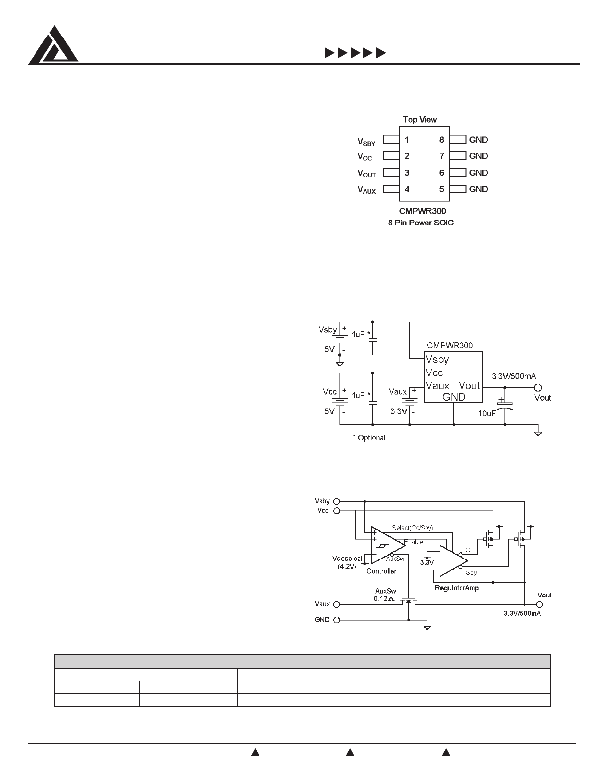
CMPWR300
500mA SmartORTM DUAL REGULATOR WITH V
Features
8-pin Power SOIC package
Continuous 3.3V output from three inputs
Complete Power Management solution
V
, V
Regulator supplies 500mA output
CC
SBY
Built-in hysteresis when selecting input supplies
Integrated switch has very low R
0.12Ω (typ.)
DS(ON)
Large Bypass Capacitors on inputs not required
Applications
PCI adapter cards with Wake-On-LAN
Network Interface Cards (NICs)
Multiple Power Systems
Systems with Standby Capabilities
Product Description
The CMPWR300 is a dual input regulator with V
switch ca-
AUX
pable of delivering 3.3V/500mA continuously. The output power
is provided from three independent input voltage sources on a
prioritized basis. Power is always taken in priority using the fol-
, V
lowing order V
, and V
CC
SBY
AUX
.
Pin Diagram
Typical Application Circuit
SWITCH
AUX
When V
ables the regulator and produces a stable 3.3V output at V
When only V
impedance direct connection (0.12Ω typ.) from V
(5V) or V
CC
is present, the device automatically en-
SBY
(3.3V) is present, the device provides a low
AUX
AUX
to V
OUT
OUT
All the necessary control circuitry needed to provide a smooth
and automatic transition between all three supplies has been
incorporated. This allows both V
and V
CC
to be dynamically
SBY
switched without loss of output voltage.
TS
RADNA
egakcaPrebmuNtraPgniredrO
sniPelytSgnikraMtraP
8rewoPCIOSAS003RWPMC
.
.
Simplified Electrical Schematic
NOITAMROFNIGNIREDROTRAPD
When placing an order please specify desired shipping: Tubes or Tape & Reel.
© 2000 Calirornia Micro Devices Corp. All rights reserved.
12/5/2000
215 Topaz Street, Milpitas, California 95035 Tel: (408) 263-3214 Fax: (408) 263-7846 www.calmicro.com
CMPWR300 is a trademark of California Micro Devices Corp.
C0621199
1
Page 2
CALIFORNIA MICRO DEVICES
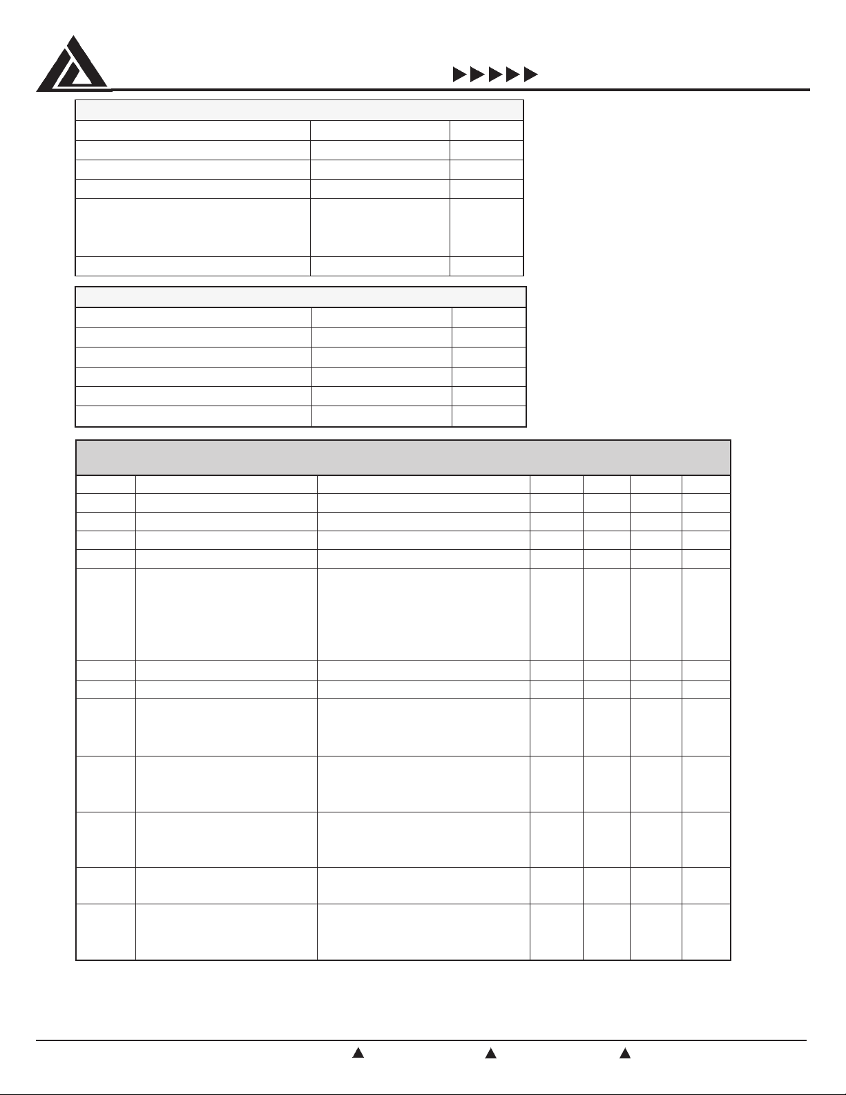
SGNITARMUMIXAMETULOSBA
retemaraPgnitaRtinU
)MBH(noitcetorPDSE0002V
V
V
CC
YBS
V
XUA
retemaraPegnaRtinU
V
V
,CC
YBS
V
XUA
tnerruCdaoL005ot0Am
C
TXE
lobmySretemaraPsnoitidnoCNIMPYTXAMTINU
V
TUO
I
TUO
V
DAOLR
V
ENILR
V
V
V
V
V
R
WS
I
C/S
I
CCR
I
YBSR
I
XUAR
I
CC
I
YBS
I
XUA
I
DNG
Note 1: The thermal resistance from junction to ambient (
Note 2: The hysteresis defines the maximum level of acceptable disturbance on
Note 3: Ground current consists of controller current and regulator current if enabled.
©2000 California Micro Devices Corp. All rights reserved.
2
V
LESCC
SEDCC
LESYBS
SEDYBS
TSYH
CC
V
CC
V
YBS
V
YBS
V
CC
V
YBS
V
V
CC
V
YBS
V
copper printed circuit board area connected to the GND pins for heat spreading, or equivalent.
215 Topaz Street, Milpitas, California 95035 Tel: (408) 263-3214 Fax: (408) 263-7846 www.calmicro.com
egatloVtupnI5.0-dnG,0.6+V
egatloVtupnI5.0-dnG,0.4+V
egnaRerutarepmeTegarotS051+ot04-
tneibmAgnitarepO07+ot0
noitcnuJgnitarepO521+ot0
1etoN
:noitapissiDrewoP
0.1W
SNOITIDNOCGNITAREPO
52.0±0.5V
3.0±3.3V
)tneibmA(erutarepmeT07+ot0
%01±01
egatloVtuptuOrotalugeRI>Am005
DAOL
tnerruCtuptuOrotalugeR 005008Am
noitalugeRdaoLV
noitalugeReniLV
I,V5=
CC
CC
DAOL
egatloVtceleS 05.406.4
egatloVtceleseDV
egatloVtceleSV
egatloVtceleseDV
2etoN
:egatloVsiseretsyH
ecnatsiseRhctiwSyrailixuAV
tnerruCtiucriCtrohSV
>V
YBS
<V
CC
XUA
YBS/CC
YBS/CC
roV
SEDYBS
SEDCC
tneserp09.302.4
VotseilppA
CC
V,V5=
TUO
egakaeLesreveRniPdnuorgotnekattupniylppusenO
egakaeLesreveRniPlamrontaniamersrehtoehtelihw505
XUA
Vnehw(
CC
Vnehw(
CC
XUA
:tnerruCdnuorG
egakaeLesreveRniPegatlov
tnerruCylppuSV
)tneserptonsiV
tnerruCylppuSV
)tneserptonsiV
tnerruCylppuSV
3etoN
V>
CC
V
TUO
YBS
V
TUO
CC
V
CC
/
V
CC
/
V
CC
I
,LESCC
DAOL
V>
SEDCC
V>
V>
SEDYBS
V>
Vro
VhtoB
CC
YBS
YBS
θ
V>
CC
CC
I
,LESYBS
DAOL
V>
V>
YBS
YBS
V>
YBS
TUO
Vdna
YBS<VTUO
Vdna
YBS
,V5=I
DAOL
,V5=I
DAOL
) must be less than 55° C/W. This is typically achieved with 2 square inches of
JA
CMPWR300
o
C
o
C
mF
SCITSIRETCARAHCGNITAREPOLACIRTCELE
)esiwrehtodeificepssselnusnoitidnocgnitareporevo(
Am0>531.303.3564.3V
Am005otAm05=02Vm
I,V5.5otV5.4=
XUA
Vdna
YBS
detcelesedera21.02.0
V0=0002Am
Am0=0.10.3
TUO
TUO
Am5=2Vm
DAOL
tneserp09.302.4V
05.406.4
noitceles03.0
Ω
µA
51.052.0Am
10.020.0
Am0=0.10.3
51.052.0Am
10.020.0
50.01.0Am
2.04.0
noitceledera51.003.0
Am0=0.10.3Am
Am005=2.15.3
V
during switching.
CC
12/5/2000
Page 3
CALIFORNIA MICRO DEVICES
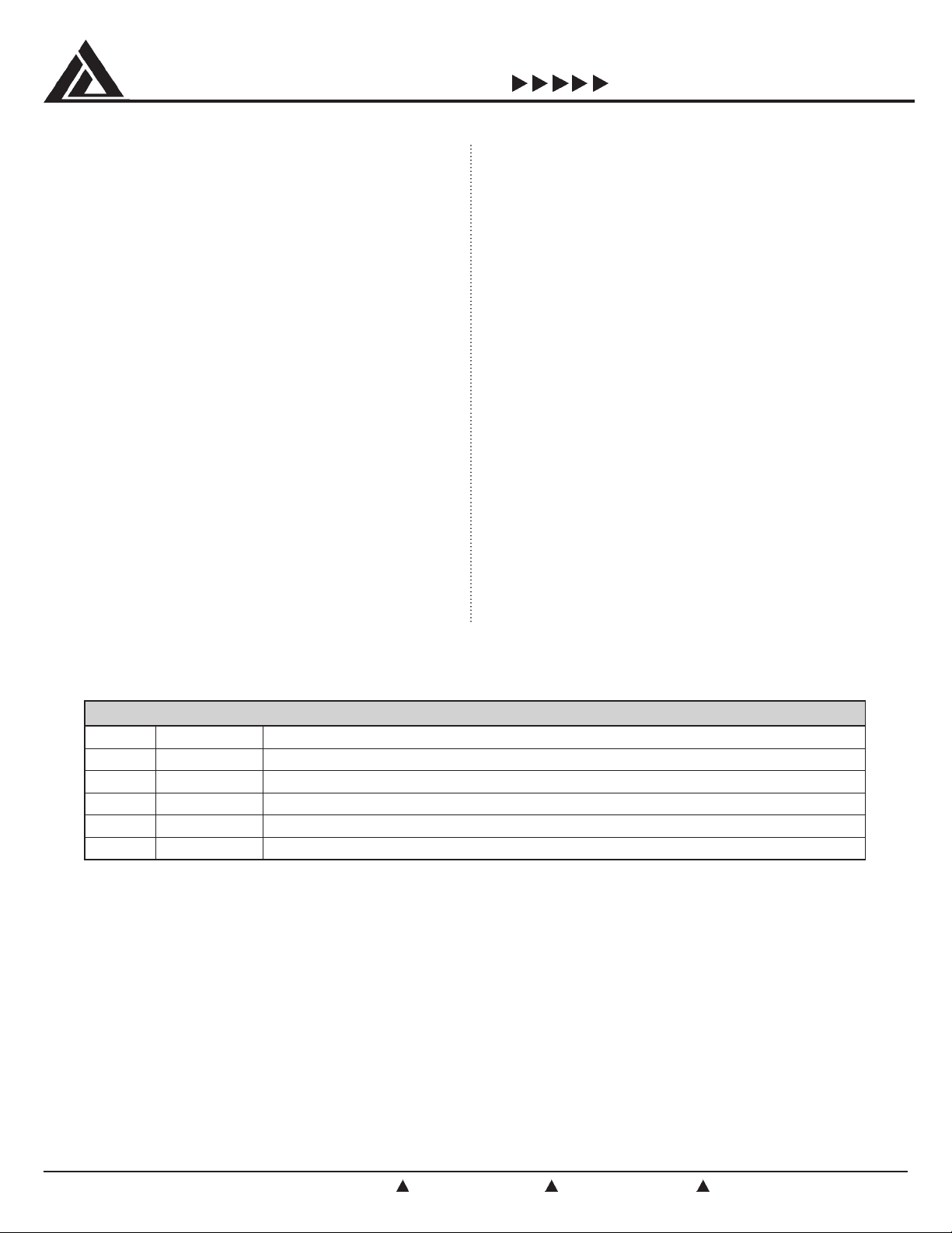
Interface Signals
V
is the primary power source which is given priority when
CC
present. If this connection is made within a few inches of
the main input filter, a bypass capacitor may not be necessary.
Otherwise a bypass filter capacitor in the range of 1µF to
10µF will ensure adequate filtering.
The voltage level on VCC is compared to an internal threshold
voltage to determine which power source is to be selected.
In order to prevent regulator dropout from occurring, the
threshold has been programmed to ensure VCC is deselected
prior to dropout, which prevents loss of output regulation
when switching between V
is set to 4.2V. Once V
voltage is immediately derived from the auxiliary power
source. To prevent chatter during this transition, the threshold
has a built-in hysteresis of 300mV which results in only V
being selected once the voltage level exceeds 4.50V
(typically).
V
is the standby 5V supply power source, which is given
SBY
priority when V
is not present. The internal regulator will
CC
remain enabled until such time that V
disable threshold level (4.2V typically). If the V
is made within a few inches of the main input filter, a bypass
capacitor may not be necessary. Otherwise a bypass filter
capacitor in the range of 1µF to 10µF will ensure adequate
filtering.
and V
CC
falls below this level, the output
CC
. Typically the threshold
SBY
falls below the
SBY
connection
SBY
CMPWR300
is the auxiliary low voltage power source. This supply
V
AUX
is only used when neither the V
these conditions an internal switch is enabled and provides
a very low impedance connection directly between V
and V
V
.
AUX
is the output voltage. Power is provided from the
OUT
regulator or via the low impedance auxiliary switch. This
output requires a capacitance of 10µF to ensure regulator
stability and minimize the peak output disturbance during
power supply changeover.
GND provides the reference for all voltages.
CC
nor V
CC
is available. Under
SBY
OUT
niPlobmySnoitpircseD
1V
2V
3V
4V
YBS
CC
TUO
XUA
8-5DNG.segatlovllarofecnerefeR
© 2000 Calirornia Micro Devices Corp. All rights reserved.
12/5/2000
215 Topaz Street, Milpitas, California 95035 Tel: (408) 263-3214 Fax: (408) 263-7846 www.calmicro.com
SLANGISECAFRETNI
Vnehwrotalugerroftupni)V5(egatlovylppusybdnatS
CC
.V2.4wolebsllaf
.rotalugerroftupni)V5(egatlovylppusyramirP
Vrehtienehwrotaluger)V3.3(tuptuoegatlovrotalugeR
Vro
CC
YBS
.tneserpsi
.hctiwsecnedepmiwolroftupni)V3.3(egatlovylppusyrailixuA
3
Page 4
CALIFORNIA MICRO DEVICES
CMPWR300
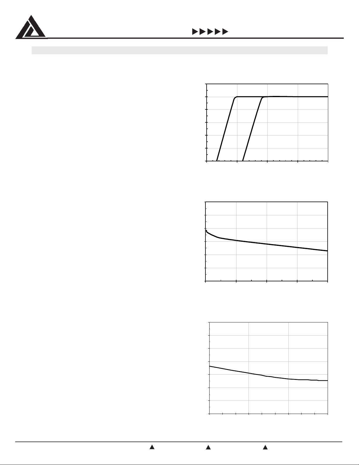
Typical DC Characteristics
Unless stated otherwise, all DC characteristics were measured at room temperature with a nominal VCC supply voltage of 5.0
volts and an output capacitance of 10µF.
Fig 1.1.
Line regulation of the regulator is shown here. At maximum
rated load conditions (500mA), a 100mV drop in regulation
occurs when the line voltage falls below 3.8V. For light load
conditions (100mA), regulation is maintained for line voltages
as low as 3.5V.
In normal operation the regulator is deselected at 4.2V, which
ensures a regulation output drop of less than 100mV is
maintained.
Fig 1.2.
Load regulation (pulse condition) performance is shown up
to and beyond the rated load. A change in load from 10%
to 100% of rated (50mA to 500mA) results in an output
voltage change of about 20mV. This translates into an
effective output impedance of less than 50mΩ.
3.35
100mA load
500mA load
3.0 3.5 4.0 4.5 5.0
Vout [V]
3.30
3.25
3.20
3.15
3.10
3.05
Vcc [V]
Fig 1.2. Load Regulation (pulse condition)
3.36
3.34
3.32
3.30
Fig 1.1. Line Regulation
Fig 1.3.
V
Switch Resistance is shown across a broad range of
AUX
supply level. From 2.7V and 3.6V, it only varies from
V
AUX
about 130mΩ down to 110mΩ.
©2000 California Micro Devices Corp. All rights reserved.
4
215 Topaz Street, Milpitas, California 95035 Tel: (408) 263-3214 Fax: (408) 263-7846 www.calmicro.com
3.28
Vout [V]
3.26
3.24
0 200 400 600 800
Load Current [mA]
Fig 1.3. Va u x S wi tch Resistance vs. Vaux
200
180
160
140
120
100
Re sistan ce [mOh m]
80
60
2.7 3 3.3 3.6
Vaux [V]
12/5/2000
Page 5

CALIFORNIA MICRO DEVICES
CMPWR300
Fig 1.4. Ground Current
Fig 1.4.
Ground Current is shown across the entire range of load
conditions. The ground current has minimal variation
across the range of load conditions and shows only a
slight increase at maximum load due to the current limit
protection circuitry.
Fig 1.5.
V
Supply Current of the device is shown across the
CC
entire V
range for both V
CC
present (3.3V) and absent
AUX
(0V).
[mA]
GND
I
10000
1000
2.0
1.5
1.0
0.5
0.0
0 100 200 300 400 500
Load Current [mA]
Fig 1. 5. Vcc Supply Current (No Load)
Vaux = 0V
In the absence of V
at approximately 1mA when V
, the supply current remains fixed
AUX
reaches the voltage level
CC
of about 2.5V. At this point the regulator is enabled and
a supply current of 1.0mA is conducted.
When V
10uA until V
powers the controller (0.15mA). When V
is present, the VCC supply current is less than
AUX
exceeds V
CC
, at which point VCC then
AUX
reaches V
CC
SELECT
the regulator is enabled.
[µA]
CC
I
100
V aux = 3.3V
,
10
12345
Vcc [V]
© 2000 Calirornia Micro Devices Corp. All rights reserved.
12/5/2000
215 Topaz Street, Milpitas, California 95035 Tel: (408) 263-3214 Fax: (408) 263-7846 www.calmicro.com
5
Page 6
CALIFORNIA MICRO DEVICES
Typical Transient Characteristics
CMPWR300
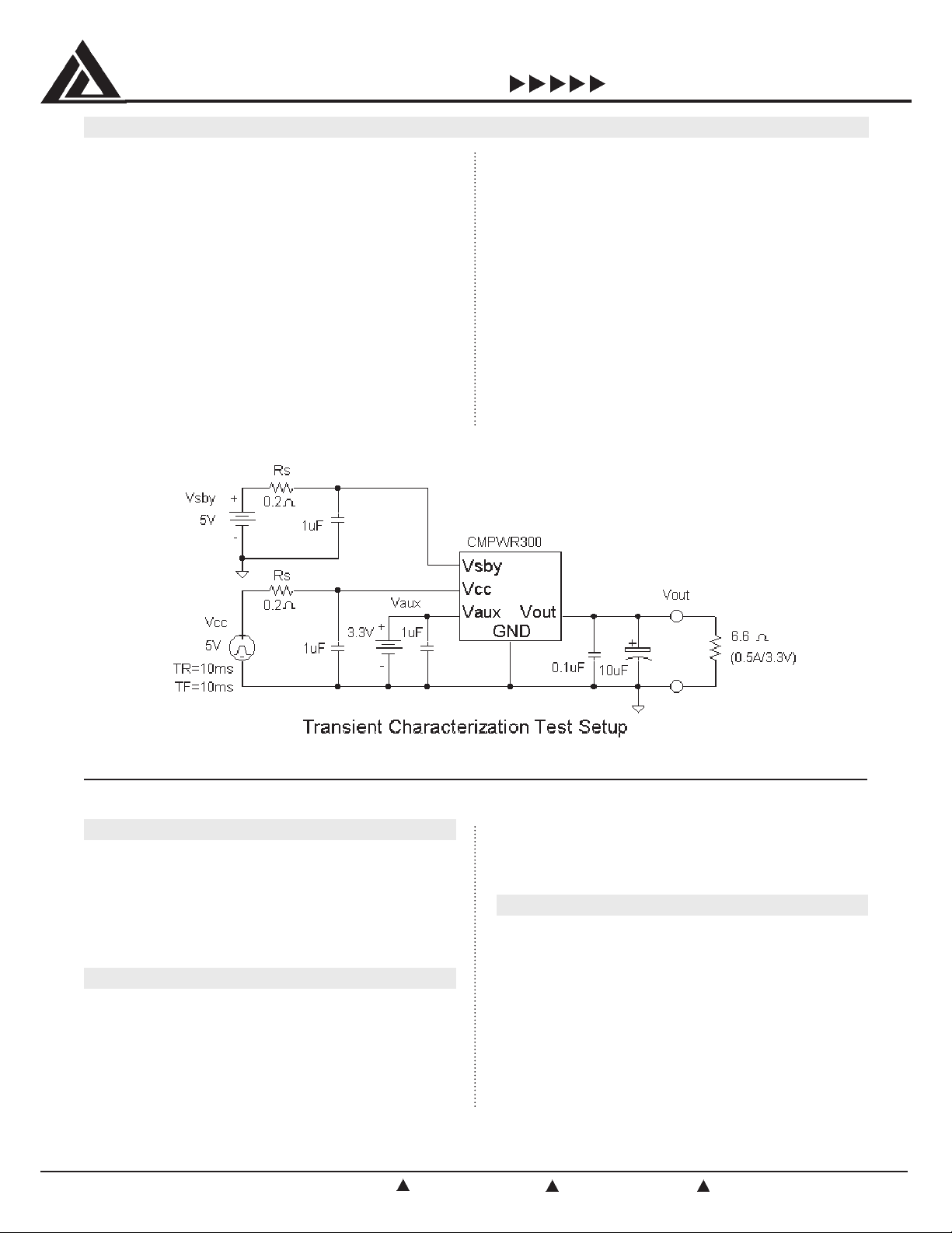
The transient characterization test setup shown below includes
the effective source impedance of the V
supply (RS). This
CC
was measured to be approximately 0.2Ω. It is recommended
that this effective source impedance be no greater than 0.25Ω
to ensure precise switching is maintained during VCC selection
and deselection.
Both the rise and fall times during V
power-up/down
CC
sequencing were controlled to be around 10 millisecond
duration. This is considered to represent worst case conditions
for most application circuits.
A maximum rated load current of 500mA was used during
characterization, unless specified otherwise.
During a selection or deselection transition the DC load current
is switching from V
. In addition to the normal load current there may also
V
CC
to VCC and vice versa, or from V
AUX
SBY
to
be an in-rush current for charging/discharging the load
capacitor. The total current pulse being applied to either
V
or VCC is equal to the sum of the dc load and the
AUX
corresponding in-rush current. Transient currents in excess
of one amp can readily occur for brief intervals when either
supply commences to power the load.
The oscilloscope traces of V
bandwidth response at the V
power-up/down show the full
CC
and V
CC
pins under full load
OUT
(500mA) conditions.
See Application note AP-211 for more details.
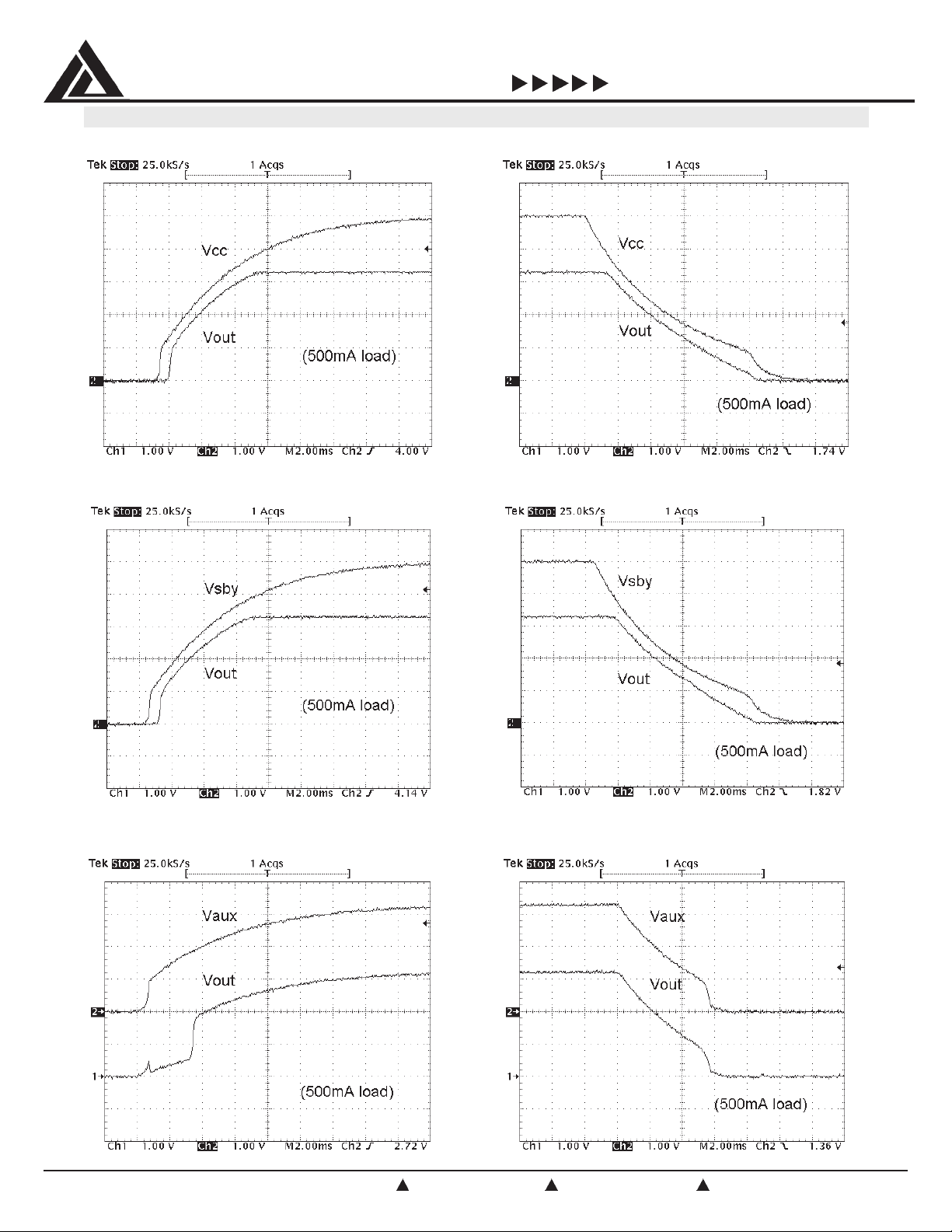
Cold Start and Full Power Down (Fig 2.1 to 2.6)
Cold start power up and power down from V
. The output voltage follows the input very smoothly
V
AUX
with no disturbance. As soon as the V
reaches about 2V, V
or V
V
CC
equals 3.8V. V
SBY
starts rising. It reaches 3.3V when
OUT
remains valid until VCC or V
OUT
CC or VSBY
drops below 3.8V.
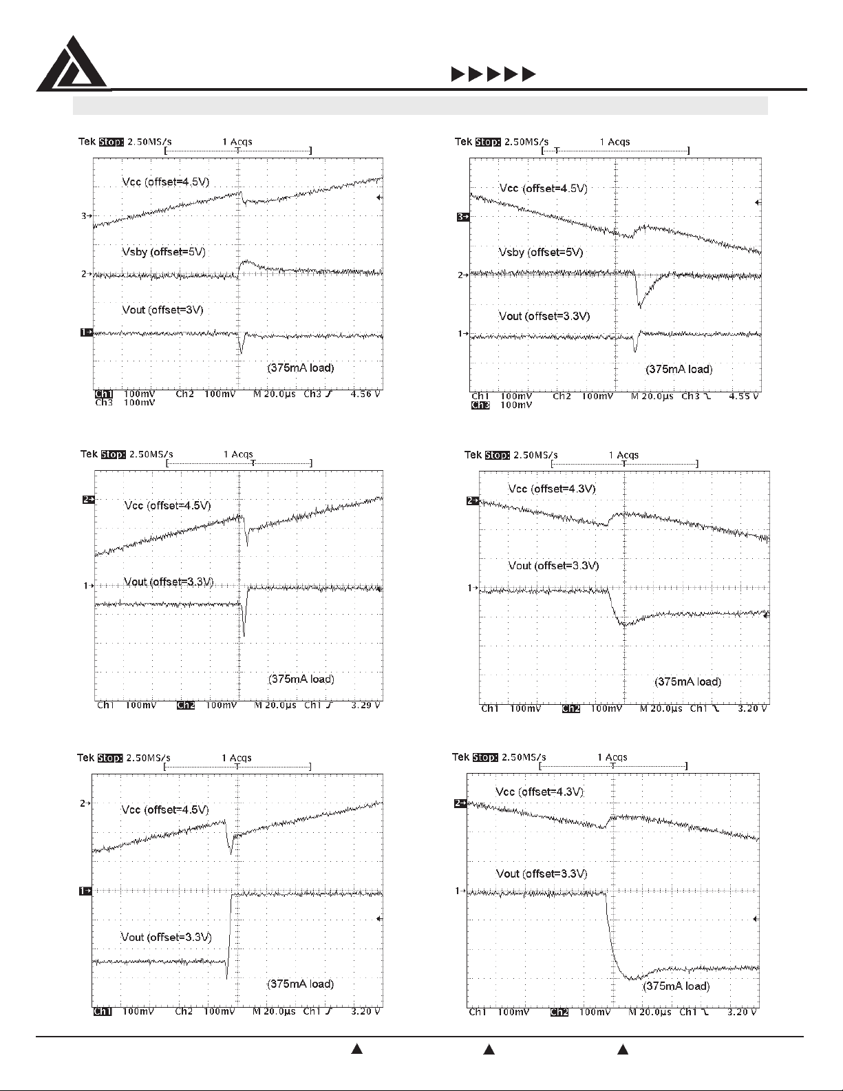
Power Changeover (Fig 2.7 to 2.12)
V
CC
Power transitions between the main V
and the standby or
CC
the auxiliary sources under 375mA load. The transition
between V
on V
OUT
and V
CC
.
Transitions between V
about 120mV on V
shows a small disturbance of 80mV
SBY
and V
CC
. During power up condition, V
OUT
show a disturbance of
AUX
experiences 100mV disturbance.
©2000 California Micro Devices Corp. All rights reserved.
6
215 Topaz Street, Milpitas, California 95035 Tel: (408) 263-3214 Fax: (408) 263-7846 www.calmicro.com
and
CC, VSBY
input voltage
SBY
This is due to the in-rush current during the power switching.
The built-in hysteresis of 300mV ensures the regulator
remains turned on throughout the transient.
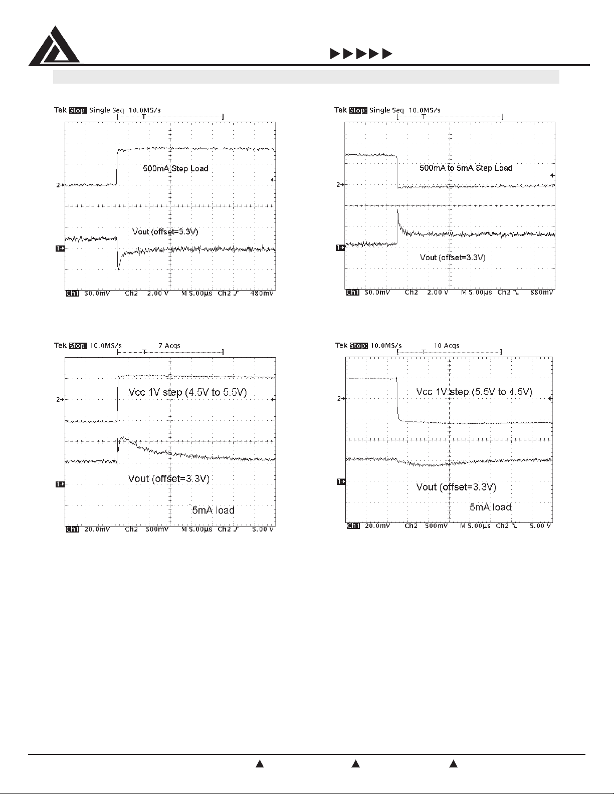
Load and Line Transient Response (Fig 2.13 to 2.16)
The load transient response shows a 5mA to 500mA step
load with minimal disturbance on V
of 80mV. An initial
OUT
transient overshoot of 80mV occurs and the output settles
to its final voltage within a few microseconds. The dc voltage
disturbance on the output is approximately 25mV, which
demonstrates the regulator output impedance of 50mW.
The line step response shows a small disturbance of 25mV
on the output when VCC steps from 4.5V to 5.5V. When
falling from 5.5V to 4.5V, the output is almost unchanged
CC
12/5/2000
Page 7
CALIFORNIA MICRO DEVICES
Typical Transient Characteristics - Cold Start and Full Power Down
CMPWR300
Fig 2.1 VCC cold start
Fig 2.3 V
cold start Fig 2.4 V
SBY
Fig 2.2 V
full power down
CC
full power down
SBY
Fig 2.5 V
© 2000 Calirornia Micro Devices Corp. All rights reserved.
12/5/2000
215 Topaz Street, Milpitas, California 95035 Tel: (408) 263-3214 Fax: (408) 263-7846 www.calmicro.com
AUX
cold start
Fig 2.6 V
full power down
AUX
7
Page 8
CALIFORNIA MICRO DEVICES
CMPWR300
Typical Transient Characteristics - V
Fig 2.7 VCC power up (V
Fig 2.9 V
power up (V
CC
Power Changeover
CC
= 5V)
SBY
= 3.3V) Fig 2.10 VCC power down (V
AUX
Fig 2.8 V
power down (V
CC
SBY
AUX
= 5V)
= 3.3V)
Fig 2.11 V
©2000 California Micro Devices Corp. All rights reserved.
8
215 Topaz Street, Milpitas, California 95035 Tel: (408) 263-3214 Fax: (408) 263-7846 www.calmicro.com
power up (V
CC
= 3.1V)
AUX
Fig 2.12 V
power down (V
CC
= 3.1V)
AUX
12/5/2000
Page 9
CALIFORNIA MICRO DEVICES
Typical Transient Characteristics - Load and Line Transient Response
CMPWR300
Fig 2.13 VCC Load Transient Response Rising
Fig 2.15 V
Load Step Response Rising Fig 2.16 VCC Load Step Response Falling
CC
Fig 2.14 V
Load Transient Response Falling
CC
© 2000 Calirornia Micro Devices Corp. All rights reserved.
12/5/2000
215 Topaz Street, Milpitas, California 95035 Tel: (408) 263-3214 Fax: (408) 263-7846 www.calmicro.com
9
Page 10

CALIFORNIA MICRO DEVICES
Typical Thermal Characteristics
CMPWR300
Thermal dissipation of junction heat consists primarily of
two paths in series. The first path is the junction to the case
) thermal resistance which is defined by the package style,
(θ
JC
and the second path is the case to ambient (θ
) thermal
CA
resistance, which is dependent on board layout.
The overall junction to ambient (θ
) thermal resistance is
JA
equal to:
= θJC + θ
θ
JA
CA
For a given package style and board layout, the operating
junction temperature is a function of junction power
dissipation P
, and the ambient temperature, resulting in
JUNC
the following thermal equation:
T
JUNC
= T
= T
AMB
AMB
+ P
+ P
JUNC
JUNC
(θ
(θ
JC
JA
) + P
)
JUNC
(θ
CA
)
The CMPWR300SA is housed in a thermally enhanced
package where the GND pins (5 through 8) are integral to
the leadframe (fused leadframe). When the device is mounted
on a double sided printed circuit board with two square
inches of copper allocated for heat spreading, the resulting
is 50°C/W.
θ
JA
Based on a maximum power dissipation of 1.0W (2Vx500mA)
with an ambient of 70°C the resulting junction temperature
will be:
T
JUNC
AMB
+ P
JUNC
(θ
)
JA
= T
= 70°C + 1.0W (50°C/W)
= 70°C + 50°C = 120°C
All thermal characteristics of the CMPWR300SA were
measured using a double sided board with two square inches
of copper area connected to the GND pins for heat
spreading.
Measurements showing performance up to junction
temperature of 125°C were performed under light load
conditions (5mA). This allows the ambient temperature to
be representative of the internal junction temperature.
Note: The use of multi-layer board construction with power
planes will further enhance the thermal performance of the
package. In the event of no copper area being dedicated for
heat spreading, a multi-layer board construction will typically
provide the CMPWR300SA with an overall θ
of 70°C/W
JA
which allows up to 780mW to be safely dissipated.
Fig 3.1. Output Voltage vs. Temperature.
This shows the regulator V
performance up to the
OUT
maximum rated junction temperature. The overall 125°C
variation in junction temperature causes an output voltage
change of about 30mV.
©2000 California Micro Devices Corp. All rights reserved.
10
215 Topaz Street, Milpitas, California 95035 Tel: (408) 263-3214 Fax: (408) 263-7846 www.calmicro.com
12/5/2000
Page 11

CALIFORNIA MICRO DEVICES
Typical Thermal Characteristics contd
Fig 3.2. Output Voltage (Rated) vs. Temperature. This
shows the regulator steady state performance when fully
loaded (500mA) in an ambient temperature up to the rated
maximum of 70°C. The output variation at maximum load is
below 10mV across the normal temperature operating.
Fig 3.3. Thresholds vs. Temperature.
This shows the regulator select/deselect threshold variation
up to the maximum rated junction temperature. The overall
125°C change in junction temperature causes a 30mV
variation in the select threshold voltage (regulator enable).
The deselect threshold level varies about 30mV over the
125°C change in junction temperature. This results in the
built-in hysteresis have a minimal variation of 40mV over
the entire operating junction temperature range. The hysteresis
increases with temperature up to 240mV at 125°C.
CMPWR300
Fig 3.2. Output Voltage (Rated) vs.
Temperature
3.320
3.310
3.300
Vout [V]
3.290
3.280
0 10203040506070
Ambient Temperature [° C]
Fig 3.3. Thre sholds vs. Te m pera ture
4.5
4.4
4.3
Threshold [V]
4.2
500mA load
Vselect
Vdeselect
Fig 3.4. V
This shows the V
Switch Resistance vs. Temperature.
AUX
switch ON resistance variation up to the
AUX
maximum rated junction temperature. The overall 125°C
change in junction temperature causes a 80mΩ variation in
the switch resistance. The switch resistance remains below
0.2Ω, even at a junction temperature of 125°C.
© 2000 Calirornia Micro Devices Corp. All rights reserved.
12/5/2000
215 Topaz Street, Milpitas, California 95035 Tel: (408) 263-3214 Fax: (408) 263-7846 www.calmicro.com
4.1
0 25 50 75 100 125 150
Junction Temperature [°C]
Fig 3.4. Vaux Switch Resistance vs.
200
160
120
80
Re sistan c e [mOh m]
40
0
0255075100125
Temperature
Junction Temperature [°C]
11
 Loading...