

Page 1
CMM2306
Features
❏ +17.5 dBm Output Power
❏ Low Current: 70 mA, Typ.
❏ 800 – 2700 MHz Operation
❏ Single +3V to +6V Supply
❏ Input and Output Matched to 50Ω, DC Blocked
❏ Low-Cost SOIC-8 Plastic Package
Applications
❏ Power Amplifier Drivers
❏ Diode-Ring Mixer Buffers
❏ PCS Medium Power Amplifiers
❏ Medium Power WLANs
❏ Base Station Receivers
Description
The Celeritek CMM2306 is a premium performance,
pin-for-pin compatible second source for the TriQuint®9132
and the Mini-Circuits®VNA. Providing higher gain and lower
noise figure than either of the existing standard amplifiers at
25% less drain current, the CMM2306 is an excellent choice
for power sensitive applications, while delivering more design
margin than either of the existing alternatives. This device
will drop into existing sockets and offers the same single supply, broadband, 50Ωmatched and DC blocked input and output features and performance, that the industry has come to
expect, with much higher efficiency and lower current.
Packaged in a low-cost surface mount SOIC-8 package, the CMM2306 offers superior performance to existing
alternatives at a competitive price.
Absolute Maximum Ratings
800 to 2700 MHz
Broadband DriverAmplifier
Parameter Rating Parameter Rating Parameter Rating
Drain Voltage (+Vd) +7 V Power Dissipation 1.0 W Operating Temperature -40°C to +80°C
Drain Current (Id) 150 mA Thermal Resistance 55°C/W Channel Temperature 175°C
RF Input Power 15 dBm Storage Temperature -65°C to +150°C Soldering Temperature 260°C for 5 Sec
Recommended Operating Conditions
Parameter Typ Units Parameter Typ Units
Drain Voltage (+Vd) 3.0 to 6.0 Volts Operating Temperature (PC Board) -40 to +70 °C
Electrical Characteristics
The following specifications are guaranteed at room temperature with drain voltage (+Vd) = 5.0 V ±5% at 2.5 GHz.
Parameter Condition Min Typ Max Units
Frequency Range 800 2700 MHz
Small Signal Gain 18.5 20 dB
Noise Figure 3.5 dB
Power Output @ 1 dB Compression 15.5 17 dBm
Output 3rd Order Intercept 27 dBm
Input Return Loss 8dB
Output Return Loss 10 dB
DC Supply Current 70 80 mA
Supply Voltage 35 6V
Product Specifications
January 1996
(1 of 4)
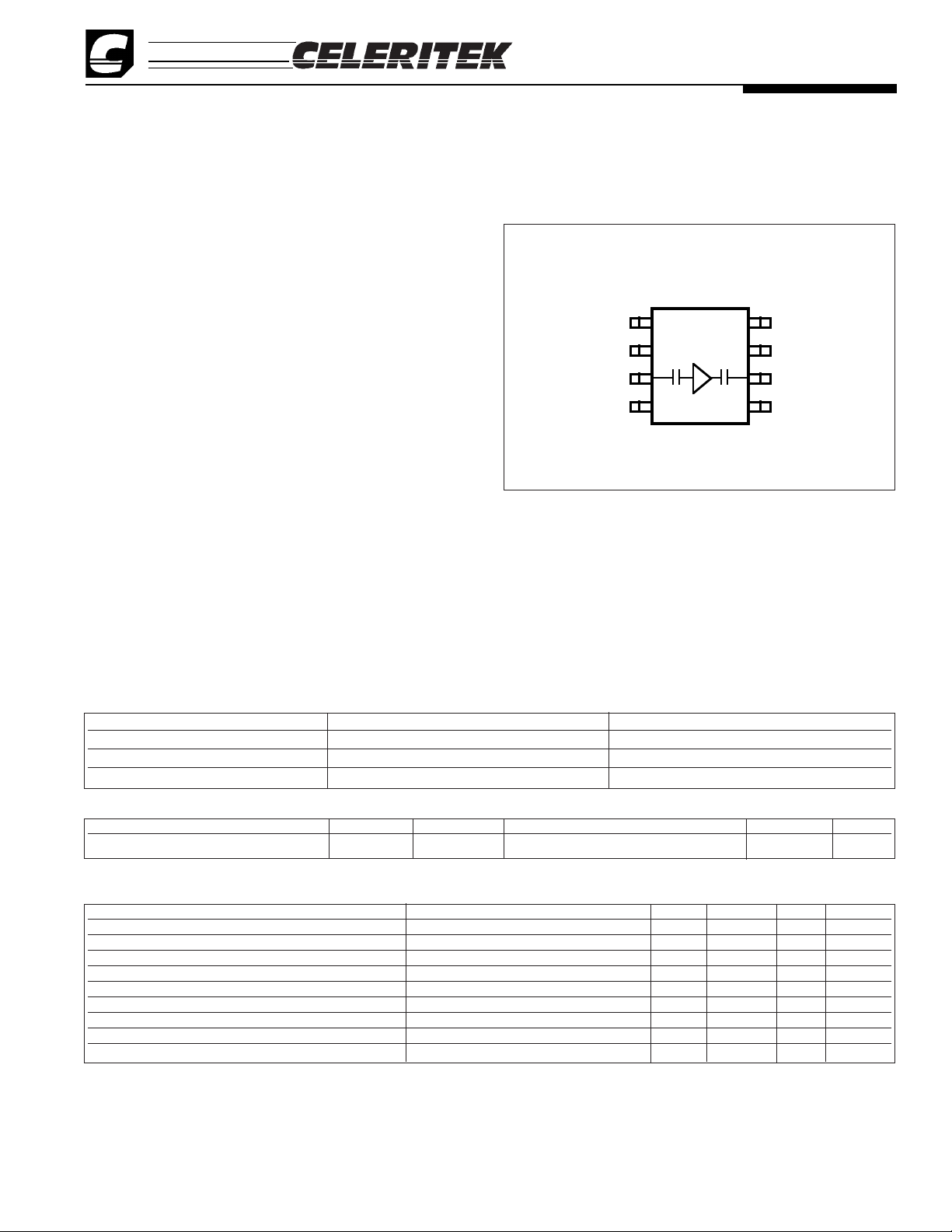
Vd 1
GND 2
RF IN 3
GND 4
8 GND
7 GND
6 RF OUT
5 GND
Functional Block Diagram
TriQuint and Mini-Circuits are trademarks of their respective corporations.
3236 Scott Boulevard Santa Clara, California 95054 Phone: (408) 986-5060 Fax: (408) 986-5095
Page 2
CMM2306
Product Specifications - January 1996
(2 of 4)
Pin # Name Description
1 +V
d
Drain voltage. Connect to positive supply.
2 GND Ground.
3 RF IN RF input (Internally DC blocked).
4 GND Ground.
5 GND Ground.
6 RF OUT RF output (Internally DC blocked).
7 GND Ground.
8 GND Ground.
Vd 1
GND 2
RF IN 3
GND 4
8 GND
7 GND
6 RF OUT
5 GND
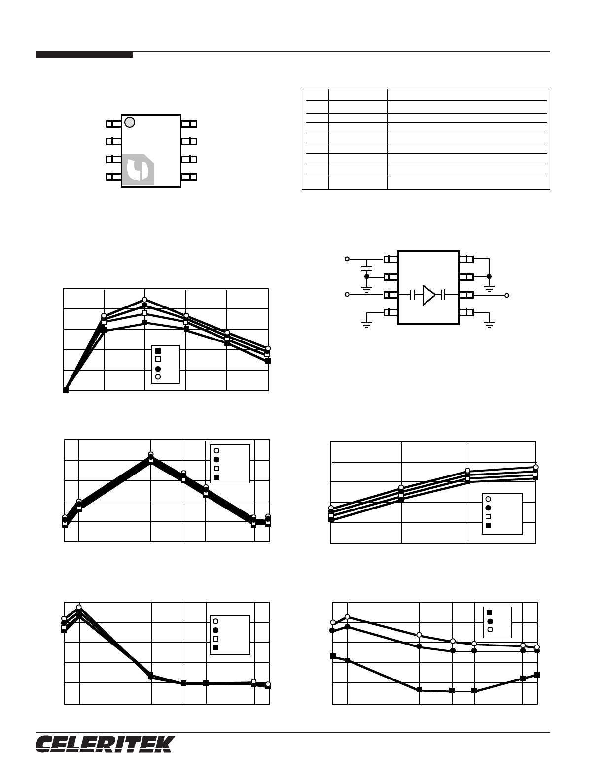
Connection Diagram and Pin Description
123 48765+5V
RF IN
0.01µF
RF OUT
Test Circuit Diagram
Typical Performance
The following typical performance parameters were tested in
the test circuit shown at room temperature and with a drain
voltage (+Vd) = 5 V, unless otherwise specified.
Frequency (MHz)
Gain vs Frequency vs V
d
Gain (dB)
101418222630500
1000
1500
2000
2500
3000
3V
4V
5V
6V
Frequency (MHz)
Gain vs Frequency vs Temperature @ 5V
Gain (dB)
1720232629
32
-20°C
0°C
+25°C
+70°C
800
900
1500
1800
2000
2500
2400
Frequency (MHz)
Power Output (P-1) vs Frequency vs Temperature @ 5V
Power Output (P-1) (dBm)
1617181920
21
-20°C
0°C
+25°C
+70°C
800
900
1500
1800
2000
2500
2400
Frequency (MHz)
Power Output (P-1) vs Frequency vs Vd @ 25°C
Power Output (P-1) (dBm)
91215182124800
900
1500
1800
2000
2500
2400
3V
5V
6V
Supply Voltage (Vd)
Gain vs Vd vs Temperature@ 1.8 GHz
Gain (dB)
202224262830345
6
-20°C
0°C
+25°C
+70°C
3236 Scott Boulevard, Santa Clara, California 95054
Phone: (408) 986-5060 Fax: (408) 986-5095
Page 3

Typical Performance (Continued)
CMM2306
Product Specifications - January 1996
(3 of 4)
Frequency (MHz)
Noise Figure vs Frequency vs Vd @ 25°C
Noise Figure (dB)
2.25
2.50
2.75
3.00
3.25
3.50
800
900
1500
1800
2000
2500
2400
3V
5V
6V
Frequency (MHz)
Noise Figure vs Frequency vs Temperature @ 5V
Noise Figure (dB)
2.25
2.50
2.75
3.00
3.25
3.50
800
900
1500
1800
2000
2500
2400
-20°C
+25°C
+70°C
Frequency (MHz)
OIP3 vs Frequency vs Temperature @ 5V
OIP3
151821242730800
900
1500
1800
2000
2500
2400
-20°C
0°C
+25°C
+70°C
Frequency (MHz)
OIP3 vs Frequency vs Vd @ 25°C
OIP3
151821242730800
900
1500
1800
2000
2500
2400
3V
5V
6V
Frequency (MHz)
S22 vs Frequency vs V
d
Output RL (S
22
)
-20
-16
-12-8-40500
1000
1500
2000
2500
3000
3V
4V
5V
6V
Frequency (MHz)
S11 vs Frequency vs V
d
Input RL (S11)
-20
-16
-12-8-40500
1000
1500
2000
2500
3000
3V
4V
5V
6V
Power In (dBm)
Power In vs Power Out & Efficiency
V
d = 4.8 V & Frequency = 1.88 GHz
Power Out (dBm)
0510152025-20
-14-8-2406121824
30
Efficiency (%)
Efficiency
Power Out
Frequency (MHz)
S12 vs Frequency vs V
d
Reverse Gain (S
22
)
-65
-55
-45
-35
-25
-15
500
1000
1500
2000
2500
3000
3V
4V
5V
6V
3236 Scott Boulevard Santa Clara, California 95054 Phone: (408) 986-5060 Fax: (408) 986-5095
Page 4

CMM2306
Product Specifications - January 1996
(4 of 4)
Physical Dimensions
Celeritek reserves the right to make changes without further notice to any products herein. Celeritek makes no warranty, representation or guarantee regarding the
suitability of its products for any particular purpose, nor does Celeritek assume any liability arising out of the application or use of any product or circuit, and specifically
disclaims any and all liability, including without limitation consequential or incidental damages. “Typical” parameters can and do vary in different applications. All operating
parameters, including “Typicals” must be validated for each customer application by customer’s technical experts. Celeritek does not convey any license under its patent
rights nor the rights of others. Celeritek products are not designed, intended, or authorized for use as components in systems intended for surgical implant into the body, or
other applications intended to support or sustain life, or for any other application in which the failure of the Celeritek product could create a situation where personal injury
or death may occur. Should Buyer purchase or use Celeritek products for any such unintended or unauthorized application, Buyer shall indemnify and hold Celeritek and
its officers, employees, subsidiaries, affiliates, and distributors harmless against all claims, costs, damages, and expenses, and reasonable attorney fees arising out of,
directly or indirectly, any claim of personal injury or death associated with such unintended or unauthorized use, even if such claim alleges that Celeritek was negligent
regarding the design or manufacture of the part. Celeritek is a registered trademark of Celeritek, Inc. Celeritek, Inc. is an Equal Opportunity/Affirmative Action Employer.
Ordering Information
The CMM2306 is available in a surface mount SOIC-8 plastic package.
Part Number for Ordering Package
CMM2306-AJ SOIC-8 surface mount narrow body plastic package
CMM2306-AJ-000T SOIC-8 package in tape and reel
Test Configuration and Evaluation
Celeritek tests the CMM2306 on an FR4 PC test
board. FR4 was chosen for its low loss characteristics at frequencies up to 2.5GHz. Plated through hole connections
from the top of the board to the backside ground plane minimizes inductance in the ground connections. These through
hole connections are as close as possible to each ground pin.
For evaluation purposes Celeritek offers a prototype
evaluation board (PB-CMM2306-AJ) for the CMM2306.
Please call the factory or a local representative for more
information.
Handling Precaution
Microwave devices are sensitive to electrostatic discharge. Proper precautions should be taken to avoid ESD
damage.
Adjacent Channel Power
π/4 DQPSK Modulation, Vd= 4.8 V
3236 Scott Boulevard, Santa Clara, California 95054
Phone: (408) 986-5060 Fax: (408) 986-5095
 Loading...