

Page 1
3236 Scott Boulevard Santa Clara, California 95054 Phone: (408) 986-5060 Fax: (408) 986-5095
CMM1530-LC
Features
❏ Operation as Low as 3.0V
❏ 38% Linear Power Added Efficiency
❏ +30 dBm Output Power (IS-136 TDMA Mode)
❏ +28.5 dBm Output Power (IS-98 CDMA Mode)
❏ 32 dB Gain at Operating Output
❏ Tested Under Digital Modulation
❏ New Low-Cost, Thermally Enhanced,
LCC-8 Package
❏ PHEMT Material Technology
Applications
❏ PCS Handsets
❏ PCS Base Stations
❏ Wireless Local Loop Subscriber Units
❏ CDMAone Handsets
Description
The CMM1530-LC is a linear power amplifier
intended for use in PCS handsets and wireless local loop subscriber units. The amplifier can be biased to meet the requirements of PCS-1900, IS-136 (TDMA), IS-98 (CDMA) or DCS1800 systems. It is a member of Celeritek’s new Triniti DX
Pro™ family of 3V power amplifier MMICs.
The CMM1530-LC is packaged in a low-cost, space
efficient, LCC-8 package that provides excellent electrical stability and low thermal resistance. The part requires minimal
external circuitry for bias and matching to reduce space and
cost.
This device is unconditionally stable under all source
and load impedances.
1.85 to 1.91 GHz
3.0V, 30 dBm, PCS/PCN
LCC-8 Power Amplifier
Advanced Product Information
November 2002
(1 of 4)
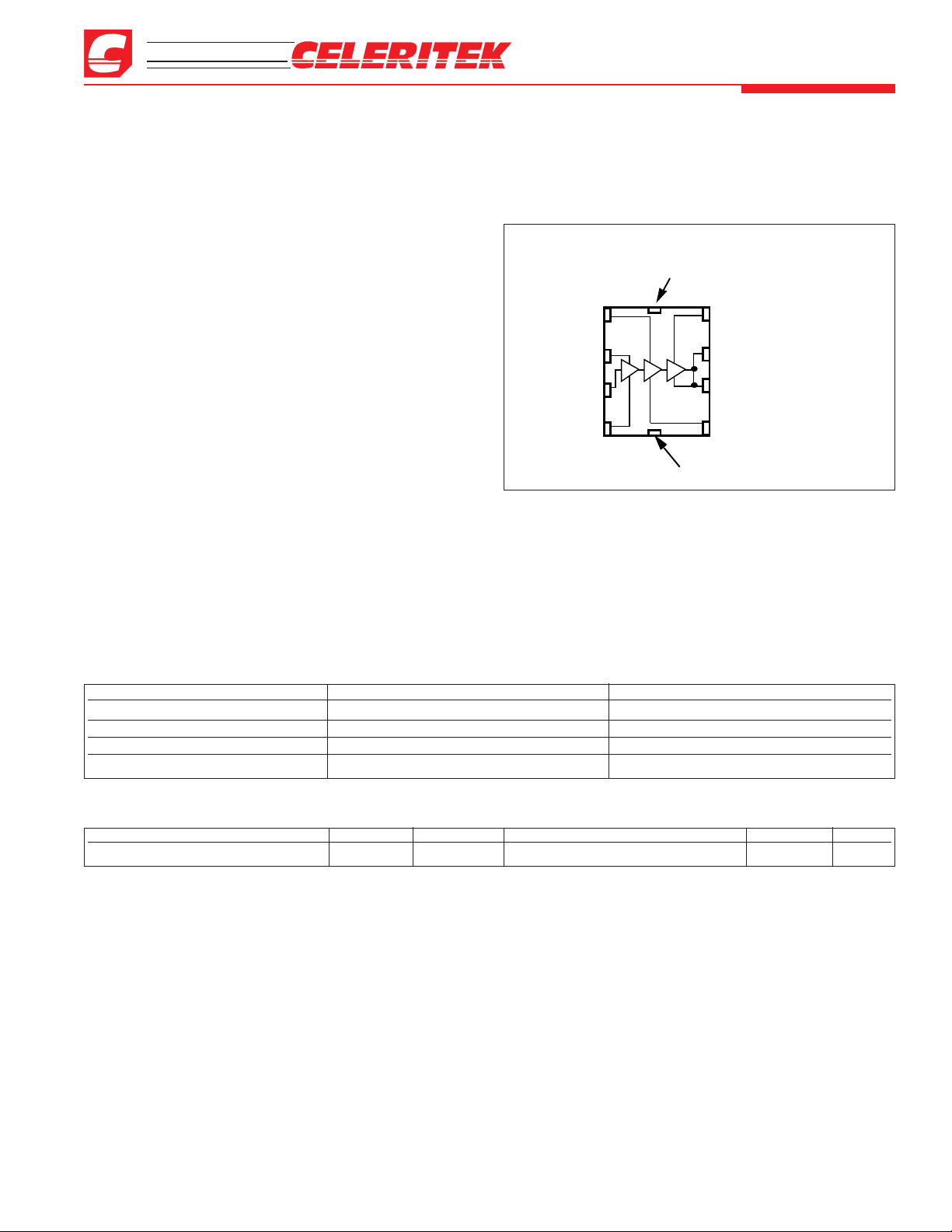
Ground Tab
Vg2 1
Vd1 4
Vg1 2
RF IN 3
7 RF OUT/V
d3
8 V
g3
5 V
d2
6 RF OUT/V
d3
Ground Tab
Functional Block Diagram
Absolute Maximum Ratings
Parameter Rating Parameter Rating Parameter Rating
Drain Voltage (+Vd) +5.5 V* Power Dissipation 5 W Operating Temperature -40°C to +90°C
Drain Current (Id) 1.8 A Thermal Resistance 20°C/W Channel Temperature 150°C
RF Input Power 3 dBm* Storage Temperature -65°C to +150°C Soldering Temperature 260°C for 5 Sec.
DC Gate Voltage (-Vg) -3.0 V*
Recommended Operating Conditions
Parameter Typ Units Parameter Typ Units
Drain Voltage (+Vd) 3.0 to 4.2 Volts Operating Temperature (PC Board) -30 to +80 °C
* Max (+Vd) and (-Vg) under linear operation. Max potential difference across the device at 1dB gain compression point (2V
d
+ |-Vg|) not to exceed the minimum breakdown voltage (Vbr) of +12V.
Application Information
The CMM1530-LC is a three stage amplifier that requires
a positive and a negative supply voltages for proper operation.
It is essential when turning on the device that the negative supply be applied before the positive supply. When turning the
device off, the positive supply should be removed before the
negative supply is removed.
The CMM1530-LC can be operated over a range of supply voltages and bias points. It is important that the maximum
power dissipation of the package be observed at all times and
that the maximum voltage across the device is not exceeded.
Circuit Design Considerations
Biasing Negative gate voltages are necessary to set the bias
currents of the three FET stages in the CMM1530-LC. The
first stage gate bias voltage is applied to Vg1 (Pin 2). The second stage gate bias voltage is applied to Vg2 (Pin 1), while the
third stage FET gate bias is applied to Vg3 (Pin 8). It is desirable to use one or more DACs (digital to analog converters)
along with appropriate divider networks, in order to adjust the
quiescent currents to within 10 mA of the target values. As an
example, for CDMA applications the target quiescent current
of the third FET is 85 mA, while those for the second and the
first FETs are 45 and 15 mA, respectively. The total quiescent
is 135 mA. It is also recommended that the quiescent currents
be set in the following sequence: the third stage FET is set
first, followed by the second stage FET, followed by the first
stage FET. The negative supply voltages control the quiescent
currents through each of the FETs and, therefore, control the
output power, adjacent channel power ratios, and the currents
at the full output power.
The positive supply voltages are applied to Pins 4, 5, 6
and 7.
– Continued on Page 2 –
Page 2
3236 Scott Boulevard, Santa Clara, California 95054
Phone: (408) 986-5060 Fax: (408) 986-5095
CMM1530-LC
Advanced Product Information - November 2002
(2 of 4)
Parameter Condition Min Typ Max Units
Frequency Range 1.85 1.91 GHz
Gain @ Digital power output 28 31 dB
Gain Ripple* 1805-1880 MHz & 1850-1910 MHz 1.5 dB
Gain Variation Over supply voltage 2 dB/V
Over temperature 0.03 dB/°C
Power Output Control Range Vdd = 0 V to +3.5 V 50 dB
Power Output Meets IS-136 TDMA mask +30.0 dBm
Meets IS-98 CDMA mask +28.5 dBm
Harmonics 2nd @ Digital power output, no output trapping, Po=+28.5 dBm -30 dBc
3rd @ Digital power output, no output trapping, Po=+28.5 dBm -40 dBc
Noise Power in Receive Band 30 kHz bandwidth -94 dBm
Linearity CDMA modulation @ +28.5 dBm Pout, 1.25 MHz offset -45 dBc/30KHz
TDMA modulation @ +30 dBm Pout - Adjacent -26 dBc
TDMA modulation @ +30 dBm Pout - Alternate -45 dBc
Spurious Signal VSWR = 3:1 in-band, VSWR = 10:1 out-of-band -80 dBc
Noise Figure 3.0 dB
Input Return Loss 10 dB
Output Return Loss 8dB
Efficiency (Vdd = 3.0 V) Pout = +30.0 dBm - TDMA 36 38 %
Pout = +28.5 dBm - CDMA 32 35 %
Positive Supply Current (Id) Pout IS-136 TDMA 750 mA
Pout IS-98 CDMA 595 mA
Quiescent Current (Iq) No RF CDMA mode 130 mA
No RF TDMA mode 200 mA
Negative Supply Current (-Ig) Includes external resistor divider 1.1 2.0 mA
Negative Supply Voltage (-Vg) Into external resistor divider -0.5 -0.8 -1.4 V
Electrical Characteristics
Unless otherwise specified, the following specifications are guaranteed at room temperature with drain voltage (+Vd) = 3.5 V in Celeritek test fixture.
* Specifications guaranteed over the temperature range of -20°C to +80°C
It is very important to provide adequate de-coupling
between the RF and DC signals in designing the DC bias circuit. Inadequate by-pass capacitance and inductance around the
DC supply lines can compromise the adjacent channel power
ratio (ACPR), or reduce power gain and/or create oscillations.
The recommend DC by-pass capacitance and low-pass in-line
inductance are shown in the evaluation board on Page 4.
Matching Circuits Output matching and input matching circuits are required to achieve the RF specifications in this data
sheet. The recommend matching circuits are identical to the
matching circuits for the evaluation board shown on Page 4.
For output power matching, one shunt capacitor along the
transmission line connected to Pins 6 and 7 as well as the bond
wire inside the package from the output leads to the output
FET are used to transform 50Ω impedance to the load line
resistance of the output FET. The placement and the value of
the capacitor are important in achieving the performance
desired. Matching circuits for the frequencies other than the
one shown can be achieved by changing the capacitor value
and the placement position of the capacitor. The device can be
designed to work from UHF to around 3 GHz.
Supply Ramping To obtain power ramping, gate supply control is recommend. Drain supply voltage ramping can also be
used.
Modulation When biased as specified, the CMM1530-LC
will achieve the required adjacent channel response for the
digital PCS system specified. Celeritek tests each product
under digital modulation to ensure correlation to customer
applications.
Thermal
1. The copper pad on the backside of the CMM1530-LC must
be soldered to the ground plane.
2. All 8 leads of the package must be soldered to the appropriate electrical connection.
– Continued from Page 1 –
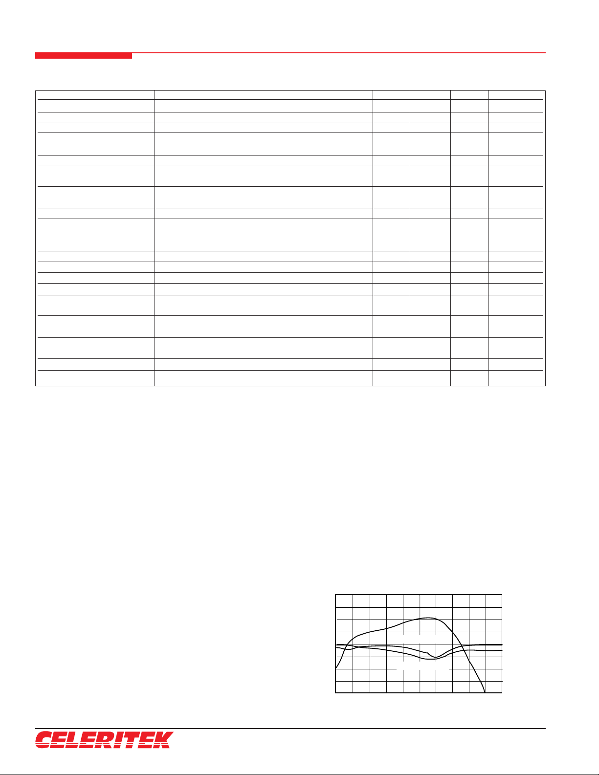
Wideband Gain & Return Loss
vs Frequency @ 3.5 V, +25°C
353025
20
Gain, dB
0.5
1.5
2.0
2.5
3.0
Frequency, GHz
-40
-30
-20
-10
0
Return Loss, dB
Gain
Input Return Loss
Output Return Loss
1.0
Typical Performance
Page 3

3236 Scott Boulevard Santa Clara, California 95054 Phone: (408) 986-5060 Fax: (408) 986-5095
CMM1530-LC
Advanced Product Information - November 2002 (3 of 4)
Typical Performance (Continued)
IS-98 CDMA Spectral Mask
(Vdd=3.5V, 1,880 MHz, Po=+28.5 dBm)
IS-136 TDMA Spectral Mask
(Vdd=3.5V, 1,880 MHz, Po=+30 dBm)
Gain & IS-136 TDMA Output Power
vs Frequency Over Voltage @ +25°C
Frequency, GHz
1.85
1.91
27
293032
Gain, dB
3.0 V
3.3 V
2.7 V
Power Out, dBm
3.0 V
3.3 V
2.7 V
TDMA Power Output and Efficiency vs Input Power
(3.0V, 1.91 GHz)
Input Output, dBm
0152535-13-117.5
Efficiency, %
Power Output, dBm
-10-7-4
52.5
35.0
Adjacent Chanel
Power Ratio, dBc
Id & IS-136 TDMA ACPR vs
Power Output (3.5V, 1.91 GHz)
Id, mA
-60
200
600
10001930
-40
-20
Adjacent channel power (worst case, Fc ±30 kHz)
Alternate channel power (worst case, Fc ±60 kHz)
21.75
24.5
27.25
Power Output, dBm (30 kHz BW)
Id
Id & IS-98 CDMA ACPR vs
Power Output (3.5V, 1.91 GHz)
Power Output, dBm (1.25 MHz BW)
-55
100
400
800
-50
-45
Adjacent channel power (worst case ±1.25 MHz)
Id, mA
0
28.5
7.125
14.5
21.625
Adjacent Chanel
Power Ratio, dBc/30 kHz
CDMA Power Output, 2nd and 3rd Harmonics
vs Input Power (3.5V, 1.91 GHz)
Input Output, dBm
-60152535-26.5
-2.5
-45
Harmonics, dBc
Power Output, dBm
5
-20.5
-14.5
-8.5
-30
2nd
3rd
Korean CDMA Spectral Mask
(Vdd=3.5V, 1,752 MHz, Po=+28.5 dBm)
Page 4

3236 Scott Boulevard, Santa Clara, California 95054
Phone: (408) 986-5060 Fax: (408) 986-5095
CMM1530-LC
Advanced Product Information - November 2002
(4 of 4)
Celeritek reserves the right to make changes without further notice to any products herein. Celeritek makes no warranty, representation or guarantee regarding the
suitability of its products for any particular purpose, nor does Celeritek assume any liability arising out of the application or use of any product or circuit, and specifically
disclaims any and all liability, including without limitation consequential or incidental damages. “Typical” parameters can and do vary in different applications. All operating
parameters, including “Typicals” must be validated for each customer application by customer’s technical experts. Celeritek does not convey any license under its patent
rights nor the rights of others. Celeritek products are not designed, intended, or authorized for use as components in systems intended for surgical implant into the body,
or other applications intended to support or sustain life, or for any other application in which the failure of the Celeritek product could create a situation where personal
injury or death may occur. Should Buyer purchase or use Celeritek products for any such unintended or unauthorized application, Buyer shall indemnify and hold Celeritek
and its officers, employees, subsidiaries, affiliates, and distributors harmless against all claims, costs, damages, and expenses, and reasonable attorney fees arising out
of, directly or indirectly, any claim of personal injury or death associated with such unintended or unauthorized use, even if such claim alleges that Celeritek was negligent
regarding the design or manufacture of the part. Celeritek is a registered trademark of Celeritek, Inc. Celeritek, Inc. is an Equal Opportunity/Affirmative Action Employer.
Ordering Information
The CMM1530-LC is available in a surface mount LCC-8 package and devices are available in tube or tape and reel.
Part Number for Ordering
Package
CMM1530-LC-00S0 LCC-8 CDMA surface mount power package in tube
CMM1530-LC-00T0 LCC-8 TDMA surface mount power package in tube
CMM1530-LC-00ST LCC-8 CDMA surface mount power package in tape and reel
CMM1530-LC-00TT LCC-8 TDMA surface mount power package in tape and reel
PB-CMM1530-LC-00S0 Evaluation Board with SMA connectors for CMM1530-LC-00S0 tested CDMA
PB-CMM1530-LC-00T0 Evaluation Board with SMA connectors for CMM1530-LC-00T0 tested TDMA
Physical Dimensions
Recommended Matching Topology
Note: This schematic represents the topology of the matching circuit recommended by Celeritek.
Evaluation Board Schematic
Board substrate:
ER = 4.60
Thickness = 0.031 in.
V
cc
TX
40 Ω 30°
@ 1.88 GHz
RF OUT
RF
IN
C1
10 µF
uuuu
uuuu
uuuu
C7
100 pF
C16
0.7 pF
50 Ω
15nH or 100 Ω
90° @ 1.88 GHz
C6
100 pF
C4
100 pF
C3
100 pF
C5
100 pF
C14
0.01 µF
C8
5600 pF
C12
0.01 µF
C9
5600 pF
C10
5600 pF
C11
0.01 µF
C2
10 µF
C13
0.01 µF
1.5 K
L2 47 nH
1.5 K
130
65
50 Ω
R5
51 K Ω
L1
47 nH
C15
3.3 pF
V
gg
1
2
3
45
6
7
8
CMM1530-LC
 Loading...