

Page 1
CM8562P
2A S
INK & SOURCE ADJUSTABLE LINEAR REGULATOR
GENERAL DESCRIPTION
The CM8562P is a low cost linear regulator designed to
provide a desired output voltage or termination voltage for
various applications by converting voltage supplies ranging
from 1V to 6.0V. The desired output voltage could be
programmable by two external voltage divider resistors.
The CM8562P is capable of sourcing or sinking up to 2A of
current while regulating an output VOUT voltage to within
2%(DDR-I) , 3% (DDR-ll) or less .
The CM8562P provides low profile 8-pin SOIC package to
save system space.
APPLICATIONS
Mother Board
PCI/AGP Graphics
Game/ Play Station
Set Top Box
FEATURES
Ideal for DDR-l、DDR-ll and DDR-lll
8-pin SOIC w/ power pad package
Source and sink up to 2A , no heat sink required
Integrated power MOSFETs
Programmable output voltage by external resistors
Output voltage could go down to 0.6V
Iccq at VCCA less than 500uA
Current limit protection and Short Circuit protection
Thermal shutdown protection
Shutdown for standby or suspend mode operation
Minimum external components
IPC
SCSI-III Bus terminator
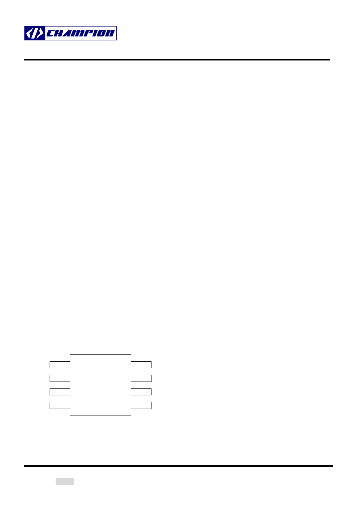
PIN CONFIGURATION
SOP-8 (S08)
Top View
1 8
2 7
3 6
4 5
VIN
GN D
GN D GN D
NC VCC A
VO U T R EF E N
2007/05/14 Rev. 0.5 Champion Microelectronic Corporation Page 1
Page 2
CM8562P
2A S
INK & SOURCE ADJUSTABLE LINEAR REGULATOR
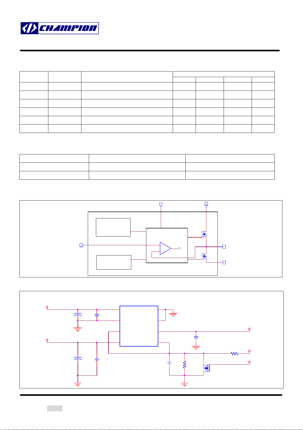
PIN DESCRIPTION
Pin No. Symbol Description
Min. Typ. Max. Unit
1 VIN Input Power 1 2.5/1.8/1.5 6 V
3 NC No Connection V
4 VOUT Output Voltage VCCA-1.9
5 REFEN
Reference Voltage Input and Chip Enable VCCA-1.9 V
6 VCCA Voltage supply for internal circuits 6 V
2,7,8 GND Ground
Operating Rating
ORDERING INFORMATION
Part Number Temperature Range Package
CM8562PIS 8-Pin SOP (S08)
CM8562PGIS* 8-Pin SOP (S08)
-40℃ to 85℃
-40℃ to 85℃
*Note : G : Suffix for Pb Free Product
BLOCK DIAGRAM
VCCA
VIN
Current Limit
Protection
REFEN
Thermal
APPLICATION CIRCUITS
VIN
CEin
200uF
VOUT
CEout
200uF
1
C3
4.7uF
2
1
C4
4.7uF
2
Control
U1 CM8562P
1
VIN
2
GND
3
NC
4 5
V TT REFEN
GND
GND
VCCA
104
8
7
6
+
-
C2
VOUT
GND
VCCA
1
C1
104
2
1
1
R2
2
100K
2
1
Q1
2 3
R1
100K
VIN
21
EN
2007/05/14 Rev. 0.5 Champion Microelectronic Corporation Page 2
Page 3
CM8562P
2A S
INK & SOURCE ADJUSTABLE LINEAR REGULATOR
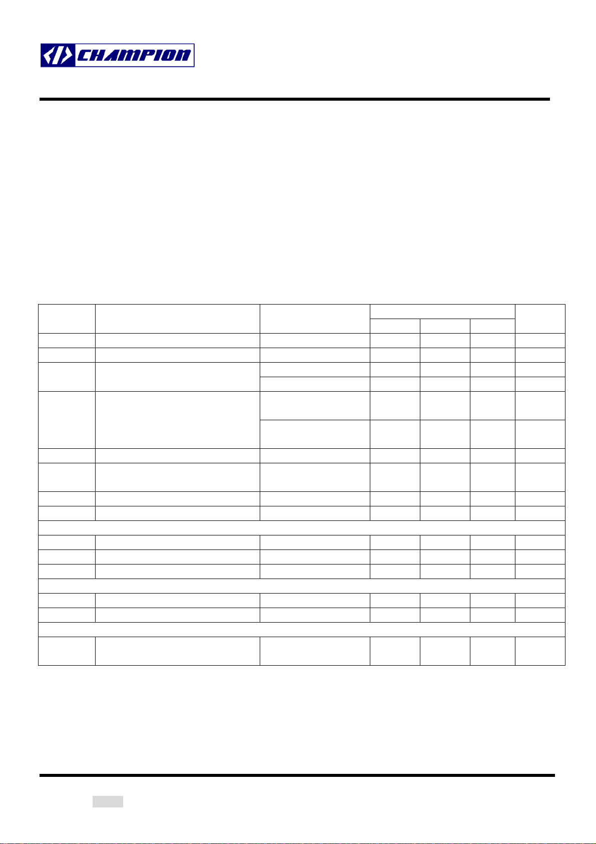
ABSOLUTE MAXIMUM RATINGS
Absolute maximum ratings are those values beyond which the device could be permanently damaged.
VIN, VCCA, VFB …................................…....……………..…..7V Lead Temperature (Soldering, 5 sec)……………….. 260°C
Output RMS Current, Source or Sink .....……………….......…...2A
Storage Temperature …….........................……. -65°C to 125°C
ELECTRICAL CHARACTERISTICS (Unless otherwise stated, these specifications apply T
VIN=+2.5V and VCCA=+3.3V, VREFEN=1.25V) maximum ratings are stress ratings only and functional device operation is not
implied. (Note 1)
Thermal Resistance(θ
Thermal Resistance(θ
)………..……… 14°C/W (PSOP-8)
JC
)…………………………… 75°C/W
JA
A
=25°C;
Symbol Parameter Test Conditions
V Output Offset Voltage I
OS OUT
I Operating Current at VIN No load, Cout=200uF 1 mA
OP
|ΔV
V Dropout Voltage
SHORT CIRCUIT PROTECTION
OVER THERMAL PROTECTION
REFEN FUNCTION
Note 1: Limits are guaranteed by 100% testing, sampling, or correlation with worst case test conditions
Note 2: VOS = VREFEN – VOUT
Note 3: Keep VCCA >= VIN and VCCA >=VREFEN + 1.9V on operation power on and power off sequences
Note 4: Guaranteed by design, not 100% test
|
LOAD
DROPOUT
I Quiescent Current at V At Room Temp. 190 230 μA
CCQ CCA
I Current in Shutdown Mode 90 110 μA
SHDN
V Input Voltage Range (Note 3) No Load 1 2.5/1.8 6 V
IN
V Input Voltage Range (Note 3) R = 10 Ohm 3.15 3.3 6 V
CCA L
I Current Limit 5 A
LIMIT
I Short Current Sinking 2 A
SC,VIN
I Short Current Sourcing 2 A
SC,GND
THSD Thermal Shutdown Temperature 3.15V<=VCCA<=6V 125 150 155
Thermal Shutdown Hysteresis 25 30 35
REFEN Threshold
Load Regulation (DDR I/II)
VREFEN < VCCA – 1.9V
=0A (Note 2) -20 20 mV
IL: 0A -> 2A 0.8/1.2 2/3 %
I
: 0A -> -2A 0.8/1.2 2/3 %
L
VCCA>VOUT+1.9V
Iout=2A
VCCA>VOUT+1.9V
Iout=1.5A
REFEN<0.2V, RL = 10
Ohm
VREFEN < VIN
Min. Typ. Max.
0.4 0.5 0.6 V
CM8562P
0.3 0.4 V
0.2 0.25 V
Unit
℃
℃
2007/05/14 Rev. 0.5 Champion Microelectronic Corporation Page 3
Page 4

CM8562P
2A S
INK & SOURCE ADJUSTABLE LINEAR REGULATOR
FUNCTIONAL DESCRIPTION
INPUTS The CM8562P is a linear regulator that is capable of sinking
and sourcing 2A of current without an external heat sink. The input voltage pins (VIN) determine the output voltages
The CM8562P integrates power MOSFETs that are capable
of source and sink 2A of current while maintaining excellent
voltage regulation. The output voltage can be regulated within
3% or less by using the external feedback. Separate voltage
supply inputs have been added to fit applications with various
power supplies for the databus and power buses.
The output voltage pins (VOUT) are tied to the databus,
address, or clock lines via an external inductor. Output voltage
is determined by the VIN.
(VOUT). At CM8562P, the desired output voltage could be
programmable by two external voltage divider resistors. VIN is
suggested to connect to VDDQ of memory module for better
tracking with memory VDDQ.
OTHER SUPPLY VOLTAGES
VCCA provide the voltage supply to the logic section and
internal error amplifiers of CM8562P. OUTPUTS
2007/05/14 Rev. 0.5 Champion Microelectronic Corporation Page 4
Page 5

CM8562P
2A S
INK & SOURCE ADJUSTABLE LINEAR REGULATOR
DIFFERENT HEATSINK AREA
Thermal Resistance vs. Different Cooper Area Layout Design
Dog-Bone Layout
Minimum Footprint , θ
Copper Area = 30mm
Copper Area = 70mm
= 75℃/W
JA
2
, θJA = 54℃/W
2
, θ
= 49℃/W
JA
2
Copper Area = 10mm
Copper Area = 50mm
, θJA = 64℃/W
2
, θ
JA
= 51℃/W
2007/05/14 Rev. 0.5 Champion Microelectronic Corporation Page 5
Page 6
CM8562P
2A S
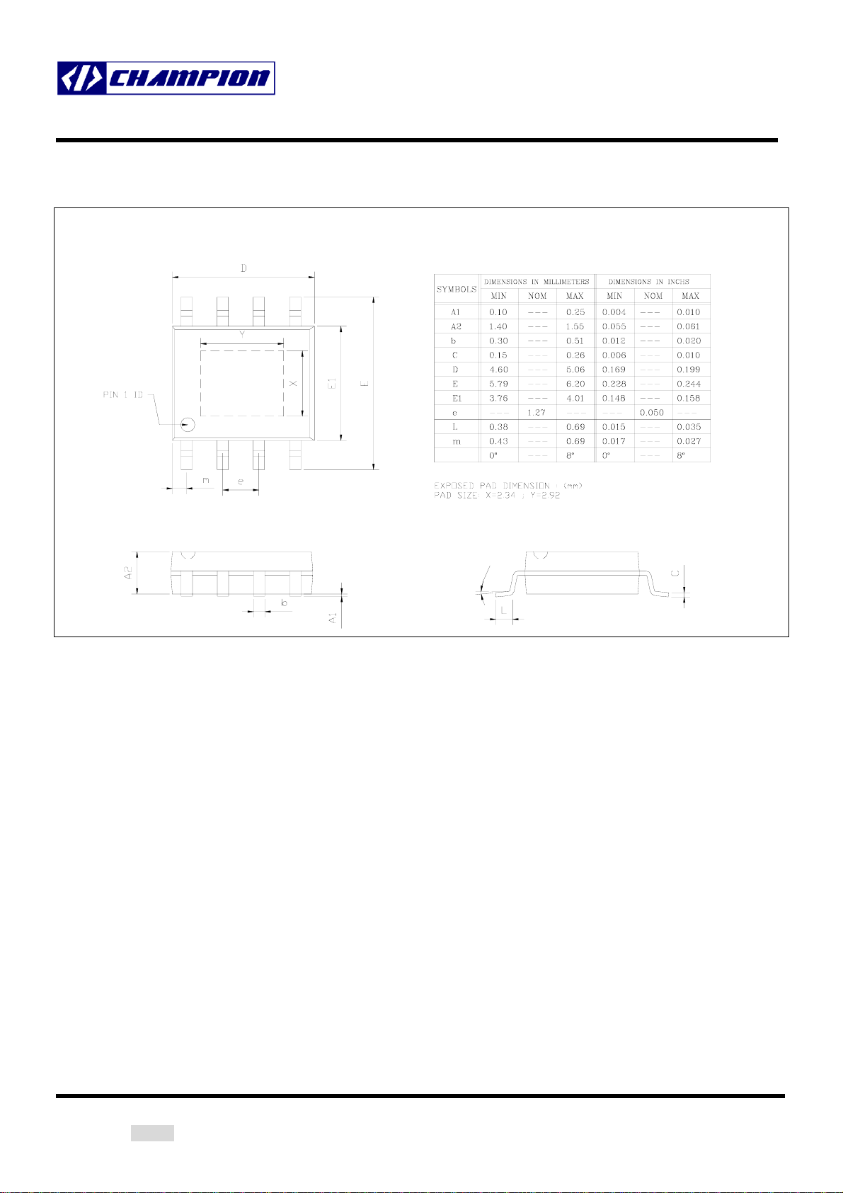
PACKAGE DIMENSION
INK & SOURCE ADJUSTABLE LINEAR REGULATOR
8-Pin SOP w/ Power Pad (PS08)
θ
θ
2007/05/14 Rev. 0.5 Champion Microelectronic Corporation Page 6
Page 7
CM8562P
2A S
INK & SOURCE ADJUSTABLE LINEAR REGULATOR
IMPORTANT NOTICE
Champion Microelectronic Corporation (CMC) reserves the right to make changes to its products or to discontinue
any integrated circuit product or service without notice, and advises its customers to obtain the latest version of
relevant information to verify, before placing orders, that the information being relied on is current.
A few applications using integrated circuit products may involve potential risks of death, personal injury, or severe
property or environmental damage. CMC integrated circuit products are not designed, intended, authorized, or
warranted to be suitable for use in life-support applications, devices or systems or other critical applications. Use of
CMC products in such applications is understood to be fully at the risk of the customer. In order to minimize risks
associated with the customer’s applications, the customer should provide adequate design and operating
safeguards.
HsinChu Headquarter Sales & Marketing
5F, No. 11, Park Avenue II, 7F-6, No.32, Sec. 1, Chenggong Rd.,
Science-Based Industrial Park, Nangang District, Taipei City 115, Taiwan
HsinChu City, Taiwan 300
T E L : +886-3-567 9979 T E L : +886-2-2788 0558
FA X: +886-3-567 9909 F A X : +886-2-2788 2985
http://www.champion-micro.com
2007/05/14 Rev. 0.5 Champion Microelectronic Corporation Page 7
 Loading...