

Page 1
CH1837A/7F/8A Data Access Arrangement Module
V.34bis High Speed DAA Module
INTRODUCTION
The Cermetek CH1837A/F Data Access Arrangement
(DAA) is designed to meet the performance
requirements of 33.6Kbps modems, such as V.34bis,
for embedded applications. The CH1837A/F meets or
exceeds the requirements for V.34 and can be used in
lower speed applications as well. The isolation voltage
and surge protection meets, as a minimum, North
American UL1950 Edition 3 (USA) and CSA C22.2
950 (Canada) requirements. Further, the CH1837A/F
has been tested to meet FCC Part 68 and is Canadian
DOT CSA CS-03 Part I approvable.
The CH1837A/F is compatible with all popular V.34bis
modem/fax chip sets. Application examples are
included in this datasheet. The CH1837A/F offers a
Quick-to-Market DAA solution for high performance
modem designs.
The CH1837A/F is exceptionally well suited for voiceover-data (VoIP) and other internet-based telephony
and data communication applications.
For those applications not requiring a two to four wire
hybrid converter circuit, the CH1838A provides all the
features of the CH1837A/F (except the hybrid
converter) while offering some cost savings. Note that
the CH1838A is a special order product only. Consult
Cermetek for availability and delivery.
FEATURES
• Low Profile
• Complete DAA function
• Compatible with most popular V.34bis modem chip
sets
• Ring detection circuitry included
• Built-in 2-wire to 4-wire conversion circuitry
(CH1837A/F only)
• UL1950 Edition 3 Listed and CSA C22.2 950
Compliant
• 1500 VAC RMS Isolation
• 2122V peak surge protection
• +5V low power operation
• Differential transmission, VoIP applications
• Compatible with V.34bis, V.32bis, V.32, V.22bis,
and V.22
• FCC Part 68 (USA) and DOT CSA CS-03 Part I
(Canada) Approvable
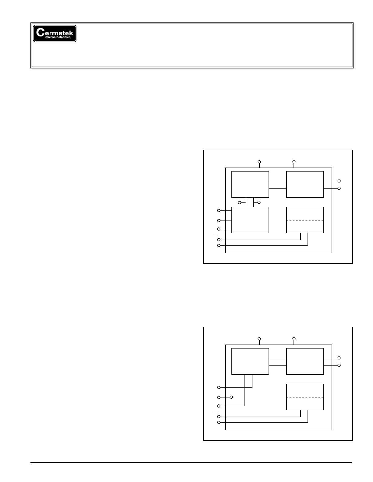
DESCRIPTION OF FUNCTIONAL BLOCKS
AND DISCUSSION OF BASIC OPERATIONS
Figure 1 contains a functional block drawing of the
CH1837A/F. Each CH1837A/F product consists of:
1) Isolation barrier.
2) Off-Hook Switch/Ring Detect circuit.
3) PSTN Line Surge and High Voltage Protection
circuitry.
4) 2-to-4 Wire Conversion circuit.
Vcc VND
ISOLATION
XMIT+
XMIT-
RCV
RI
OFFHK
T1
HYBRID
2W/4W
CONVERTER
T2
Figure 1. Function Block Diagram of CH1837A/F.
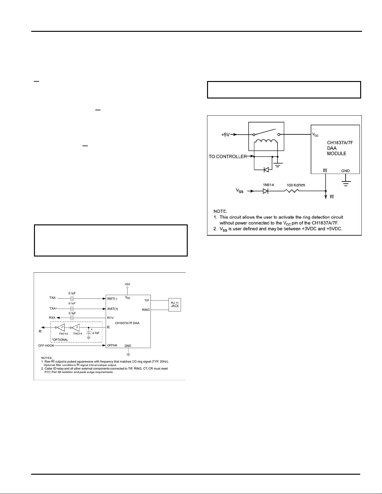
Figure 2 contains a functional block drawing of the
CH1838A. Each CH1838A product consists of:
1) Isolation Barrier.
2) Off-hook Switch/Ring Detect circuit.
3) PSTN Line surge and High Voltage Protection
Circuitry.
Vcc VND
ISOLATION
T2
N/C
T1
RI
OFFHK
N/C
Figure 2. Function Block Diagram of CH1838A.
SURGE AND
PROTECTION
CIRCUITRY
OFF HOOK
RING DET.
SURGE AND
PROTECTION
CIRCUITRY
OFF HOOK
RING DET.
TIP
RING
TIP
RING
2002 Cermetek Microelectronics, Inc. Page 1 Document No. 607-0014 Revision C2 (12/02)
Page 2
Cermetek Microelectronics, Inc. CH1837A/7F/8A Data Access Arrangement Module
Ring Detection. To announce an incoming call, the
telephone company’s central office (CO) applies an
AC ringing signal to the PSTN line. The
CH1837A/7F/8A is designed to detect this signal. The
CH1837A/7F/8A uses the AC ring signal to produce a
square wave pulse train output at the CH1837A/7F/8A
RI pin. This pulse train is the same frequency as the
incoming AC ring signal and is typically 20 Hz. Figure
3 shows external filtering which may be employed to
provide an envelope indication of the ring signal using
the CH1837A/7F/8A RI output. The ring detection
When the OFFHK input is TTL High, the
CH1837A/7F/8A is Off-Hook. The Off-Hook state
indicates to the CO that the CH1837A/7F/8A is either
answering a call or preparing to place a call.
OFFHK Input: Active HIGH
OFFHK active Current: 5mA
circuit in the CH1837A/7F/8A family is designed to
deter false indications caused by pulse dialing or noise
on the PSTN line.
Additionally, the RI output of the CH1837A/7F/8A is
diode protected thereby allowing an external pull-up
resistor (R>100k ohms) to +5V to be utilized to
activate the ring detection circuit when the
CH1837A/7F/8A is not connected to power. This can
be handy for designs in which power consumption is of
concern. When circuited in this manner, there is
virtually no current draw until a ring signal is present.
Refer to Figure 4.
RI Output: Opt coupler, 30KΩ pull-up, Active
LOW
Square wave 15-68HZ (TIP. 20Hz)
Sensitivity: 38Vrms across TIP and RING
Figure 4. Low Power Ring Detection Circuit.
2-Wire to 4-Wire Hybrid Converter (CH1837A/F
only). This circuit block performs two functions:
1. It applies the XMIT signal to the PSTN line, and
2. It subtracts the XMIT signal from the total signal
present on the PSTN line thereby deriving the
RCV signal.
The accuracy of the RCV signal derivation depends on
how closely the impedance of the PSTN line matches
an ideal 600 Ohms. Generally, a small amount of the
XMIT signal will appear at RCV due to the non-ideal
nature of the PSTN line impedance. The ratio of the
applied XMIT signal to the received XMIT signal is
called Trans-Hybrid Rejection, or Trans-Hybrid Loss.
PSTN Line Isolation and Surge/Peak Voltage
Protection. The Public Switched Telephone Network
(PSTN) line isolation barrier circuitry provides isolation
Figure 3. Typical Application.
Hook Switch Control.
The OFFHK input is used to toggle the
CH1837A/7F/8A from On-Hook to Off-Hook and back
to On-Hook.
When the OFFHK input is TTL Low, the
CH1837A/7F/8A is On-Hook. The On-Hook state
indicates to the CO that the CH1837A/7F/8A is ready
to receive calls.
and the required surge and high voltage protection.
This circuitry effectively isolates the user’s equipment
from both the PSTN line and the CO. The
CH1837A/7F/8A has been designed to meet both FCC
Part 68 (USA) and DOT CSA CS-03 Part I (Canada)
isolation and surge requirements when circuited as
indicated in Figure 5. Among the more critical
parameters, the PSTN isolation barrier will provide at
least 1500VAC RMS isolation and 2122V peak surge
protection. The CH1837A/7F/8A is also UL1950
Edition 3 listed and meets CSA C222-950 test
conditions when connected as indicated in Figure 5.
2002 Cermetek Microelectronics, Inc. Page 2 Document No. 607-0014 Revision C2 (12/02)
Page 3

Cermetek Microelectronics, Inc. CH1837A/7F/8A Data Access Arrangement Module
TRANSMIT SIGNALS
The CH1837A/7F/8A does not attenuate the transmit
signal before it applies the signal across tip and ring.
Therefore, a transmit signal of –9dBm applied to XMIT
will comply with the FCC Part 68 requirement for data
signals across Tip and Ring.
CH1837A/F. The user presents all outgoing transmit
signals to the XMIT(-) pin with respect to GND for
single ended operation or between XMIT(-) and
XMIT (+) for differential operation. This signal must be
AC coupled through a 0.1µF capacitor present on both
the XMIT(-) and XMIT(+) pins as shown in Figure 3.
For single-ended operation, the outgoing analog signal
is applied to the XMIT(-) pin with respect to GND. This
signal must be AC coupled using a 0.1µF capacitor as
shown in Figure 3. In single ended signal operation,
the XMIT(+) pin must be connected to GND through a
0.1µF capacitor.
CH1838A. All incoming and outgoing signals are
presented between T1 and T2. The user must provide
an external hybrid conversion circuit and/or control the
flow of the transmit and receive signals into/from the
CH1838A.
RECEIVE SIGNALS
The incoming analog signal appears across TIP and
RING. The CH1837A/7F/8A does not amplify the
receive signal. Receive signals can vary from a
maximum strength of -9dBm to below -50dBm.
CH1837A/F. The CH1837A/F derives the incoming
signal and presents it at RCV with respect to GND.
The user must AC couple RCV through a 0.1µF
capacitor as indicated in Figure 3.
CH1838A. The CH1838A presents the incoming
signal between T1 and T2. The user must provide an
external hybrid conversion circuit and/or control the
flow of the transmit and receive signals into/from the
CH1838A.
Attenuation: 0.0dN
Input Impedance: 150KΩ
Typical Input Signal: 0dBm or 0.775Vrms with the
Signal referenced to GND and
AC coupled
UL RECOGNITION
To further protect the end product containing the
CH1837A/7F/8A from field failures caused by large
transients present on poor quality PSTN lines and to
maintain UL recognition, an additional level of external
transient protection is required. Refer to Figure 5 for
mandatory additional protection circuitry.
DESIGN CONSIDERATIONS
The CH1837A/7F/8A DAA includes circuitry that
couples the modem signals to the PSTN line and
provides the FCC required voltage isolation and surge
protection when circuited per Figure 5 herein.
Cermetek offers the following end product design
guidelines as suggestions only. These guidelines are
intended to facilitate the usage of Cermetek DAA
modules and to assist the user with FCC certification
of their end product.
1. Mount the DAA in the final assembly so that it is
isolated from exposure to any hazardous voltages
within the assembly. Adequate separation and
restraint of cables and cords must be provided.
2. Connect to the PSTN line through a standard FCC
approved RJ-11C jack or equivalent. For RJ-11,
use the two center pins.
3. All PCB traces from the CH1837A/7F/8A TIP and
RING pins must be at least 0.1 inch spacing from
all other traces or other conducting material. The
purpose for this spacing is to maintain 1500 VC
isolation between the incoming PSTN line and the
other traces. PSTN related PCB Traces should
have a width of 0.020 inches or greater.
4. TIP and RING PCB traces should be as short as
possible and should be oriented to prevent direct
or induced coupling with other signals present on
the PCB.
5. The CH1837A/7F/8A processes signals in the
millivolt range. Even though the CH1837A/7F/8A
is designed to handle noise in the power supply,
steps should be taken to assure that the noise
level does not exceed 50 mV peak-to-peak.
Particular attention should be paid to both the
power supply and the ground line PCB traces.
6. For data calls, FCC Part 68 rules require silence
on the PSTN line for at least 2 seconds after a
data call has been completed to allow central
offices to exchange billing information. Further,
Part 68 specifies that the transmit level must not
exceed -9dBm.
7. For voice calls, the FCC rules require that the end
product must meet the requirements of Part 68 for
Out-of-Band Energy, and DTMF Transmit Levels.
2002 Cermetek Microelectronics, Inc. Page 3 Document No. 607-0014 Revision C2 (12/02)
Page 4

Cermetek Microelectronics, Inc. CH1837A/7F/8A Data Access Arrangement Module
HANDLING AND ASSEMBLY
RECOMMENDATIONS
The CH1837A/7F/8A DAA Module contains staticsensitive components and should only be handled by
personnel and in areas that are properly protected
against static discharge. Industry standard ESD and
EOS procedures and precautions should be observed
when handling CH1837A/7F/8A products.
DOT (CANADA) REGISTRATION
The CH1837A/7F/8A DAA meets or exceeds the
hazardous voltage, surge and leakage requirements of
the FCC when circuited per the requirements of Figure
5 herein. Although the FCC and DOT requirements
are virtually identical, it is recommended that for
applications that connect to Canadian PSTN lines, a
Canadian test house/consultant be retained to ensure
compliance of the end product.
MOUNTING THE DAA
There are two mounting techniques recommended for
physically connecting the CH1837A/7F/8A DAA to a
PCB:
1. Direct soldering.
2. Sockets.
Direct Soldering. The CH1837A/7F/8A may be wave
soldered onto a circuit card. All CH1837A/7F/8A
products are hermetically sealed and will not be
harmed by industry standard wave soldering
processes.
To avoid the problems of flux contamination, hand
soldering is preferred to wave soldering. When
cleaning, use only demonized water.
Socketing. The socketing approach to mounting
eliminates cleaning and desoldering concerns. When
the socket is used, it must make a solid connection to
all pins. Failure to do so will cause unreliable or
intermittent operation.
When using sockets, steps should be taken to assure
that the DAA module remains tightly seated in the
socket after the end product is shipped. It is
recommended that some type of mechanical restraint
be provided to keep the CH1837A/7F/8A seated to
avoid any possibility that the CH1837A/7F/8A works
loose during shipment. See Application Note # 130,
Summary of Recommended Suppliers
recommended socket manufacturers.
for a list of
FCC (USA) REGISTRATION
Because the CH1837A/7F/8A already meets the FCC
requirements for Part 68 registration for High Voltage
Isolation and Surge Protection when circuited per the
requirements of Figure 5 herein, certification of the end
product containing the CH1837A/7F/8A DAA is
normally quite simple. The process involves testing
the end system for compliance and submitting the test
data to the FCC for review.
Typically, independent FCC approved testing labs are
contracted to perform the required tests on the end
product and to submit the required paperwork to the
FCC. If desired, Cermetek can assist with the
Registration activity.
2002 Cermetek Microelectronics, Inc. Page 4 Document No. 607-0014 Revision C2 (12/02)
Page 5

Cermetek Microelectronics, Inc. CH1837A/7F/8A Data Access Arrangement Module
Table 1. CH1837A/F Pin Description.
PIN I/O CH1837A/F FUNCTION
1 I/O TIP TIP. Direct PSTN line connection.
2 I/O RING RING. Direct PSTN line connection.
3 I OFFHK OFF-HOOK. Used to toggle CH1837A/F product between On-Hook and Off-Hook.
When set LOW, CH1837A/F is On-Hook. When set HIGH, CH1837A/F is set OffHook to answer or place a call. See Note 1.
4 O RI RING INDICATION. Indicates the presence of a ring signal between TIP and RING
pins. RI output is a square wave coincident with the incoming AC ring signal. The
RI square wave output can be conditioned to produce an envelope of the incoming
AC ring signal by using the circuit in Figure 4. See Notes 2 and 3.
5 O RCV RECEIVE. Audio output signal with respect to GND. AC couple RCV through
0.1µF capacitor to eliminate any DC offset.
6 I XMIT(-)
TRANSMIT(+). Audio input signal. AC couple through 0.1µF capacitor. The
CH1837A/F can be used in differential mode with XMIT(+) or in single ended mode
with respect to GND.
7 I VCC
POWER SUPPLY. +5V±5%. Supply line noise should be less than 50mV peak to
peak.
8 I XMIT(+) TRANSMIT(-). Audio input signal for CH1837A/Fwhen used in differential mode
only. Connect to GND through 0.1µF capacity when CH1837A/F used in single
ended input via PIN 8.
9 I GND GROUND. Supply line noise should be less than 50mV peak to peak.
Note:
1. When answering incoming calls in response to a ring indication on RI, internal degradation may occur if OFFHK
is set HIGH before RI returns to its HIGH state.
2. For CH1837A, the RI output is 2X the frequency of the incoming ring signal.
3. For CH1837F, the RI output is 1X the frequency of the incoming ring signal.
Table 2. CH1838A Pin Description.
PIN I/O CH1838A FUNCTION
1 I/O TIP TIP. Direct PSTN line connection.
2 I/O RING RING. Direct PSTN line connection.
3 I OFFHK OFF-HOOK. Used to toggle CH18378 product between On-Hook and Off-Hook.
When set LOW, CH1838 is On-Hook. When set HIGH, CH1838 is set Off-Hook to
answer or place a call. See Note 1.
4 O RI RING INDICATION. Indicates the presence of a ring signal between TIP and
RING pins. RI output is a square wave coincident with the incoming AC ring
signal. The RI square wave output can be conditioned to produce an envelope of
the incoming AC ring signal by using the circuit in Figure 4. The RI output is 2X
the frequency of the incoming ring signal.
5 I/O T1 RECEIVE. Audio input and output signal with respect to T2.
6 N/C N/C AUDIO INPUT/OUTPUT. Internally not connected. Either let float or connect to
GND.
7 I VCC
POWER SUPPLY. +5V±5%. Supply line noise should be less than 50mV peak to
peak.
8 I/O T2 AUDIO INPUT/OUTPUT. Audio input and output signal with respect to T1.
9 I GND GROUND. Supply line noise should be less than 50mV peak to peak.
Note:
1. When answering incoming calls in response to a ring indicator on RI, internal degradation may occur if OFFHK
is set HIGH before RI returns to its HIGH state.
2002 Cermetek Microelectronics, Inc. Page 5 Document No. 607-0014 Revision C2 (12/02)
Page 6

Cermetek Microelectronics, Inc. CH1837A/7F/8A Data Access Arrangement Module
Table 3. CH1837A/7F/8A Electrical Specifications.
Parameter Conditions Min. Typ. Max. Units
Logic
Input HIGH
Input LOW
Input Leakage HIGH
Input Leakage LOW
Output HIGH
Output LOW
IOH=0.05mA
IOL=2.0mA
2.4
3.0
0.4
500
-500
0.4
V
V
µA
µA
V
V
Isolation Protection
Between TIP and
CH1837A/7F/8A
1500
VAC RMS
RING
Surge Protection
Between TIP and
CH1837A/7F/8A
2212
V
Peak
RING
Transmission Insertion Loss Attenuation between the transmitter input
PSTN line at 1.8kHz with 600ohms
-0.8 0
+0.8
dB
termination (flat from 300-4kHz)
Frequency Response
(Ref=1800Hz Transit)
200-4kHz
-0.3
+0.3
dBm
Distortion Noise-Transmit -10dBm transmit power (600Hz) -82 dBm
Receive Gain Gain between PSTN line and receive output
-0.5 0 +0.5 dB
at 1800Hz with 600 ohm resistive termination
(flat from 300-4kHz)
Receive Frequency Response
(Ref = 1800Hz Receive)
Receive 2nd/3rd/4th
200-4kHz
-0.3
+0.3
dBm
-10dB at TIP and RING -82 dBm
Harmonic Distortion
Noise-Receive 400Hz-4kHz -82 dBm
PSTN Line Input Impedance At 1800Hz 550 600 650 Ohm
On-Hook Impedance 10 20 mOhms
Loop Current 48VDC from TIP to RING. 20 100 mA
Longitudinal Balance OH=0 (On-Hook)
OH=1 (Off-Hook)
Return Loss
1kHz 25 dBm
66
66
dBm
dbm
(Zref=600ohm, 2.16µF)
Trans-Hybrid Loss Attenuation between the transmitter input
22 25 dB
and receiver output at 1kHz with 600ohm
complex termination
Transmit Input Impedance At 1800Hz 120 150 200 kOhm
Receive Output Impedance At 1800Hz 10 100 Ohms
Ring Select Sensitivity AC voltage between TIP and RING 38 V
rms
Hook Switch Control Current Drive capable of sourcing current 4 mA
Weight 20 gm
Supply Current
V
=+5VDC±5%, Off-Hook
CC
V
=+5VDC±5%, On-Hook
CC
5 8 mA
mA
Ringer Equivalence Type A 0.2A REN
2002 Cermetek Microelectronics, Inc. Page 6 Document No. 607-0014 Revision C2 (12/02)
Page 7

Cermetek Microelectronics, Inc. CH1837A/7F/8A Data Access Arrangement Module
Figure 5. PSTN Line Interface.
1. Currently Limiting PSTN Protection Line
Device.
Currently limiting devices are mandatory to meet
UL safety standards. For FCC Part 68 approval,
the current limiting components identified as F1
and F2 in dashed Box #1 must also survive FCC
Part 68 surge testing. Refer to Cermetek
Application Note #126, Supplemental PSTN Line
Protection, for more details. Refer to Application
Note # 130, Summary of Recommend Suppliers,
for a list of suppliers and associated part numbers.
A. A Polyfuse (rated at 0.15 amps) is preferred
because it resets automatically upon removal
of the current flow. Non-resettable devices
are also acceptable. Refer to Application Note
#130 for a complete list of recommended
vendors and associated part numbers.
B. Resistors (10Ω carbon film or 1/8 watt
minimum) may be used in Canada, as Canada
has no requirements that PSTN equipment be
operational after a Type B surge test.
C. Although CSA CS-03 Part 1 (Canada) follows
the requirements of FCC Part 68 (USA),
Cermetek recommends contacting DOT
(Canada) and/or a certified independent lab to
verify compliance. For Canada, use either
10Ω resistors (carbon film or SMD parts 1/8
watt minimum) as described in paragraph B
above.
2. Over Voltage and Lightning Protection.
A. The required UL1950 and FCC Part 68 surge
protection (identified as D1 in dashed Box 2)
must be supplied externally. The purchaser
must include some form of surge protection as
described herein to obtain FCC Part 68
3. EMI/RFI Suppression.
approval and to maintain UL1950 Edition 3
listing.
B. In most environments, 2 terminal surge
suppressors are adequate. For severe
environments, use an external 3 terminal
device (as indicated in Figure 5) with an earth
ground.
Additional suppression, if required, may be added
as described below in Sections 3A-3B without
adversely affecting FCC Part 68 approval or
UL1950 listing.
A. To provide adequate EMI/RFI suppression,
the capacitor/inductor network contained in
dashed Box #3 should be located as close to
the RJ11 Jack as possible. Further, this
network should be provided with an excellent
ground path to the chassis.
B. Capacitors C1 and C2 should not exceed
0.005µf. They must have a rating of 1.5KV
and typically are 0.001µf ± 20%. Inductors L1
and L2 may be either individual inductors or a
dual inductor. Refer to Application Note #130
for a complete list of recommended vendors
and associated part numbers. For UL
applications, choose capacitors and inductors
that are UL 1950 listed. The actual values of
the components used may vary depending on
the end product design.
2002 Cermetek Microelectronics, Inc. Page 7 Document No. 607-0014 Revision C2 (12/02)
Page 8

Cermetek Microelectronics, Inc. CH1837A/7F/8A Data Access Arrangement Module
Table 4. Summary CH1837A/7F/8A Product Features.
Model Summary of Features Operating Temperature
CH1837A 33.6kbps DAA, 2-to-4 Wire Conversion, FCC Part 68 Compliant, UL 1950
0°C to +70°C
Edition 3 Listed. RI is 2X the incoming ring frequency.
CH1837F 33.6kbps DAA, 2-to-4 Wire Conversion, FCC Part 68 Compliant, UL 1950
0°C to +70°C
Edition 3 Listed. RI is 1X the incoming ring frequency.
CH1838A 33.6kbps DAA, FCC Part 68 Compliant, UL 1950 Edition 3 Listed Special
0°C to +70°C
Order Option to Standard CH1837A/F product.
Notes:
1. Pins are 0.010 inches X 0.020 inches.
*2. Nominal pin length is 0.200 inches for CH1837A/8A.
*3 Nominal pin length is 0.155 inches for CH1837F.
4. Nominal case tolerance ± 0.02 inches.
5. Nominal pin tolerance ± 0.03 inches.
Figure 6. Physical Dimensions.
Cermetek reserves the right to make changes in specifications at any time and without notice. The information furnished by
Cermetek in this publication is believed to be accurate and reliable. However, Cermetek assumes no responsibility for its use, or for
any infringements of patents or other rights of third parties resulting from its use. No license is granted under any patents or patent
rights of Cermetek.
406 TASMAN DRIVE | SUNNYVALE CA 94089 | LOCAL: 408-752-5000 | TOLL FREE: 1-800-882-6271 | FAX: 408-752-5004
CERMETEK WEB SITE:
iModem Network WEB SITE:
http://www.cermetek.com | EMAIL: sales@cermetek.com
http://press4service.cermetek.com/ or https://press4service.alanet.net/
Printed in U.S.A
2002 Cermetek Microelectronics, Inc. Page 8 Document No. 607-0014 Revision C2 (12/02)
Page 9

Cermetek Microelectronics, Inc. CH1837A/7F/8A Data Access Arrangement Module
2002 Cermetek Microelectronics, Inc. Page 9 Document No. 607-0014 Revision C2 (12/02)
 Loading...