

Page 1
CH1817
Family of Low Profile DAA Modules
INTRODUCTION FEATURES
The CH1817 is a Family of Low Profile Data Access
Arrangement (DAA) Modules. They are compatible
with all modem chip sets. These devices have been
tested to meet or exceed FCC Part 68 requirements
and are Canadian DOC approvable. They are also
recognized by Underwriters Laboratories to UL 1459
Specifications.
The CH1817 modules are ultra small (1.0” x 1.0”
x0.35”) affording an easy integration into spacesensitive designs, including laptop and hand-held
computer based products. The CH1817 family of
products may be socketed or mounted directly onto a
Printed Circuit Board (PCB). The telephone line
connection is made through TIP and RING to an RJ-11
jack or equivalent.
The CH1817 is intended for use with FAX/modem chip
sets that have a data throughput of up through
V.32bis. For High Speed Applications, Cermetek
recommends the CH1837A.
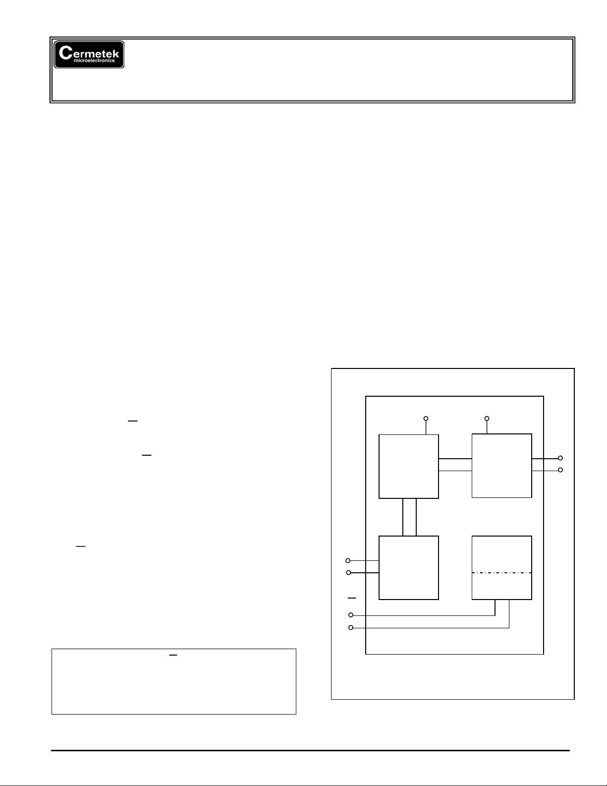
FUNCTIONAL DESCRIPTION
Ring Detection. Referring to the block diagram in
Figure 1, incoming ring detection is performed by the
CH1817 and the RI pin is set Low during the 2 second
(typical) ring period and is restored to High for the 4
seconds (typical) between rings. During incoming ring
signal activity, the RI output is pulsed at the same
frequency as the ringing signal, typically 20Hz. Figure
2 contains additional external circuitry which may be
used to provide an envelope indication of the ring
signal. The internal ring detection circuit is designed
to deter false indications due to pulse dialing or noise
on the line.
The RI output of the CH1817 is diode protected.
Therefore, an external pull-up resistor (R>100Kohm)
to +5V may be utilized to activate the ring detection
circuit when the CH1817 is not connected to power.
This can be handy in designs where power
consumption is of concern. When circuited in this
manner, there is virtually no current draw until a ring
signal is present.
• Low Profile, Ultra small size: 1.0” x 1.0” x 0.35”
• Complete DAA function
• Ring detection
• Built-in 2-wire to 4-wire conversion
• Lightweight
• Multimedia compatible
• +5V operation
• 1000 VAC isolation
• 800 Volt surge protection
• V.32bis/14,400bps, applications
• UL1459 recognized
• CH1817-L: Low power consumption and Common
mode noise rejection filter
• CH1817-LM (special order): Reduced transmit
attenuation
• CH1817-D: Differential transmission input and 0dB
transmission insertion loss.
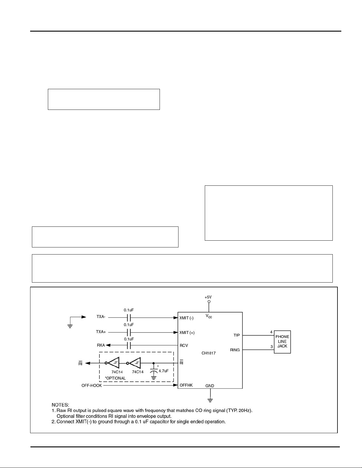
ISOLATION
XMIT
RCV
RI
OFFHK
CONVERTER
VCC
HYBRID
2W/4W
GND
SURGE
AND
PROTECTION
CIRCUITRY
OFF-HOOK
SWITCH
RING DET.
TIP
RING
RI
Output: Active low
Opto coupler, 30KΩ pull-up
Square wave: 15-68Hz (Typ. 20Hz)
Sensitivity: 38Vrms across Tip & Ring
Figure 1. CH1817 DAA Functional Block Diagram.
2002 Cermetek Microelectronics, Inc. Page 1 Document No. 607-0007 Revision B (01/02)
Page 2
Cermetek Microelectronics, Inc. CH1817 Family of Low Profile DAA Modules
Hook Switch. The OFFHK input is used to control the
on-hook and off-hook status of the CH1817. When
OFFHK is low, the CH1817 is in the On-Hook State.
This indicates to the CO that the CH1817 is ready to
receive calls. When OFFHK is high, the CH1817
allows the CO supplied loop current to flow, indicating
either it is answering a call or preparing to place a call.
OFFHK
Input: Active High
Active Current: 4mA
2-Wire To 4-Wire Hybrid Converter. This block has
TRANSMIT SIGNAL
The outgoing analog signal to be transmitted through
the phone line should be applied to the XMIT pin (with
respect to GND) and must be AC coupled as shown in
Figure 2. For the CH1817-D a XMIT (+) and XMIT (-)
pins provide a differential input. The CH1817-L
attenuates the transmit signal by 9.5dB, 0dB for the –D
option. Therefore, a transmit signal of 0dBm for the –L
option (-9.5 dB for –D) applied to XMIT will comply
with the FCC Part 68 requirement for data signals of –
9dBm across TIP and RING.
two functions: RECEIVE SIGNAL
1. It applies the XMIT signal to the phone line.
2. It subtracts the desired signal from the total
outgoing signal on the phone line to derive the
RCV signal.
The accuracy of this derivation depends on how
closely the impedance of the phone line matches 600
Ohms. Generally, a small amount of the XMIT signal
will appear at RCV. The ratio of the applied XMIT
signal to the received XMIT signal is called TransHybrid Rejection, or Trans-Hybrid Loss. On a 600Ω
phone line, the CH1817 DAAs have very high transhybrid rejection, typically 23 dB.
NOTE
The FCC requires that the DTMF tone not exceed
0dBm.
The incoming analog signal appearing between TIP
and RING is presented at RCV with respect to GND
and must be AC coupled to the user equipment
receive input. The CH1817 does not gain the receive
signal. Receive signals can vary from a maximum
strength of –9dBm to below –50dBm.
RCV
Gain: 0dB
Out impedance: 100Ω
Typical Output Signal:
-9dBm to –50dBm
2.5Vrms to 0.27mVrms
Signal referenced to GND
AC coupling required
XMIT CH1817-D CH1817-L CH1817-DM CH1817-LM Attenuation 0dBm 9.5dBm 6.5dBm 6.5dBm Input Impedance
150KΩ 150KΩ 150KΩ 150KΩ
Figure 2. Typical CH1817 Application.
2002 Cermetek Microelectronics, Inc. Page 2 Document No. 607-0007 Revision B (01/02)
Page 3
Cermetek Microelectronics, Inc. CH1817 Family of Low Profile DAA Modules
Table 1. CH1817 Family Pin Description.
Pin Name I/O Function
1
TIP
I/O TIP. Direct telephone line connection.
2
3
4
5
6
7
RING
OFFHK
RI
RCV
XMIT(-)
or
N/C
VCC
I/O RING. Direct telephone line connection.
I
OFF HOOK. When set LOW, the CH1817 is placed On-Hook. When set HIGH, the
CH1817 is placed Off-Hook to answer or place a call. This input can also be used
for pulse dialing. NOTE: When answering incoming calls in response to a ring
indication on RI, internal relay contact degradation may occur if OFFHK is set HIGH
before RI returns to its HIGH state.
O
RING INDICATION. It is asserted LOW by the CH1817 during the 2 second ON
portion of the incoming AC Ring Signal and is asserted HIGH during the 4 second
idle period between rings. An envelope of the AC ring signal may be created using
the application circuit shown in Figure 2.
O
RECEIVE. This provides the signal or audio output with respect to ground and must
be AC coupled with a 0.1µF capacitor to eliminate DC offset.
I
TRANSMIT SIGNAL (-). Input a differential AC coupled audio signal with respect to
or
XMIT(+), CH1817-D versions only. All others, No Connection. For single ended
-
operation of CH1817-D, connect this pin to ground through a 0.1µF capacitor.
I
POWER SUPPLY. +5V ± 5%
8
XMIT(+)
I
TRANSMIT SIGNAL (+). Input an AC coupled audio signal with respect to ground.
Input a differential signal with respect to XMIT(-) for the CH1817-D versions only.
9
GND
I
Ground. Must be connected to signal ground. Note: Noise should be less than
25mV peak-to-peak.
2002 Cermetek Microelectronics, Inc. Page 3 Document No. 607-0007 Revision B (01/02)
Page 4

Cermetek Microelectronics, Inc. CH1817 Family of Low Profile DAA Modules
CH1817-L: LOW POWER
The L Family is a Low Power version of the CH1817
DAA. When Off-Hook, this DAA draws only 4mA
through Vcc. When On-Hook, the L Family can be
configured so that the Ring Detection circuit can be
activated by a pull-up resistor on RI while Vcc has
been disconnected from the power supply, thus
making the On-Hook power consumption virtually zero
(See Figure 4).
CH1817-D: 0 dB XMIT ATTENUATION
The D option has 0.0 dB insertion loss (typical) with
respect to a differential input between XMIT (-) and
XMIT (+). This allows the maximum signal strength of
–9dBm to be input while maintaining FCC compliance.
To use the CH1817-D as single end input device,
ground the XMIT (-) pin through a 0.1uF capacitor.
MOUNTING THE DAA
The DAA can be soldered directly to the host circuit
card or installed in sockets. To avoid the problems of
contamination, hand soldering is preferred to wave
soldering. When hand cleaning use only deionized
water; when wave soldering use washless flux.
DESIGN CONSIDERATIONS
The CH1817 DAA includes circuits that couple the
modem signals to the phone line and provides FCC
required isolation and protection. The FCC
registration process by the host product can be
minimized provided that the following guidelines are
followed.
1. The mounting of the DAA in the final assembly
must be made so that it is isolated from exposure to
any hazardous voltages within the assembly.
Adequate separation and restraint of cables and
cords must be provided.
2. Connection to the phone line should be made
through a standard FCC approved RJ-11C jack or
equivalent.
3. Circuit board traces from the DAA’s TIP and RING
pins must exceed 0.1 inch spacing from all other
5. The DAA Module is a sensitive subsystem that
should be treated as any other integrated
component. Pay special attention to the power
supply to the DAA. The device handles signals in
the millivolt range. Even though it is designed to
handle noise in the power supply, steps should be
taken to assure the noise level does not exceed
50mV peak-peak.
6. For data calls, Part 68 rules require silence on the
phone line for at least 2 seconds after a data call
has been completed to allow central offices to
exchange billing information and specifies the
transmit level must not exceed -9dBm. The FCC
rules also require that for voice calls the final
system meet the requirements of Part 68 for Out-of
Band Energy, and DTMF Transmit Levels.
Because the CH1817 already meets FCC
requirements for Part 68 registration for High
Voltage isolation and Surge Protection, the
certification of the product is normally a simple
process that often can be completed directly with
the FCC. If desired, independent testing labs are
available that can test the system and submit the
required paperwork to the FCC for approval.
Cermetek can assist with the registration.
7. The CH1817 DAA as is meets or exceeds the
hazardous voltage, surge and leakage
requirements of the FCC. For applications that
connect to Canadian phone lines, governed by the
DOC (Department of Communications) and to
further protect the CH1817 from field failure on
excessively poor quality lines and to maintain UL
recognition, a higher level of transient protection is
required, thereby making mandatory the circuit
consisting of two fuses and one varistor as shown
in Figure 3. Adding these three devices will not
affect FCC registration. Components L1, L2, C1,
C2 are optional and serve two purposes. First, they
restrict high frequency signals from reaching the
phone line and thereby add EMI protection.
Second, they protect against externally generated
RFI from degrading the modem’s ability to operate
on proper carrier signals. Adding these devices will
not affect FCC, DOC, or UL registration.
traces or other conducting material. The purpose
for this pacing is to maintain 1000 VAC isolation
between the phone line and the other traces.
Traces should have a nominal width of 0.020
inches or greater.
4. TIP and RING traces should be as short as
possible and should be oriented to prevent direct or
induced coupling with other signals on the host
circuit card.
2002 Cermetek Microelectronics, Inc. Page 4 Document No. 607-0007 Revision B (01/02)
Page 5

Cermetek Microelectronics, Inc. CH1817 Family of Low Profile DAA Modules
Figure 3. Telephone Line Interface.
1. RJ-11 Jacks must be provided by one of the
vendors on the list. Refer to Application Note
#130, Summary of Recommended Suppliers
.
2. Current Line Device: F1 and F2 – 1.25amp.
A. UL 1459 must use a current limit device. A
Poly Fuse is recommended as this device
resets automatically after each power surge.
B. Resistors (10ohm carbon film or SMD 1/8W
minimum) may be used for non UL
applications.
3. Over Voltage and Lightning Protection.
A. DOC (Canada) may require external current
limiting devices. Use 1ohm resistors (carbon
film or SMD parts 1/8W minimum) in each lead
(TIP and RING). You may substitute fuses or
the Poly Fuse described in Section 2.
Figure 4. Low Power Ring Detection.
B. For lightning prone areas where there are
more than 2 storms per year, provide an earth
ground connection and use a three terminal
sidactor or similar device that provides metallic
and longitudinal protection. This must also
include the current protection in Section 2.
4. EMI/RFI Suppression.
The capacitor/ inductor network should be located
as close to the RJ-11 Jack as possible with an
excellent ground path to the chassis. Capacitors
C1 and C2 should not exceed 0.005µF. They
must have a rating of 1.5KV and typically have a
value of 0.001µF ± 20%. Inductors L1 and L2 are
ferrite cylinders and provide attenuation to high
frequencies from system level components
external to the CH1817. The required values must
be empirically determined for each product design
2002 Cermetek Microelectronics, Inc. Page 5 Document No. 607-0007 Revision B (01/02)
Page 6

Cermetek Microelectronics, Inc. CH1817 Family of Low Profile DAA Modules
Table 2. CH1817 DAA Electrical Specifications.
V
=+5VDC ± 5%, TA=0° to 55°C
CC
Parameter Conditions Min. Typ. Max. Units
Supply Current Off-Hook
Off-Hook
Transmission
Insertion Loss
Attenuation between transmit input and telephone line at
1800Hz with 600Ohm termination:
CH1817-L measured XMIT(+) with respect to GND
CH1817-DM measured XMIT(-) with respect to XMIT(+)
CH1817-LM measured XMIT(+) with respect to GND
CH1817-D measured XMIT(-) with respect to XMIT(+)
Receive Gain Gain between telephone line and receive output at
4
0.6
9.0
6.0
6.0
-0.5
9.5
6.5
6.5
0.0
6
1.5
10.0
7.0
7.0
0.5
mA
mA
dBm
dBm
dBm
dBm
-0.5 0.0 0.5 dBm
1800Hz with 600Ohm termination
Telephone Line
At 1800Hz 550 600 650 Ohm
Input Impedance
Trans-Hybrid Loss Attenuation between the transmitter input and receiver
18 23 dBm
output at 1800Hz with 600Ohm termination
Transmit Input
At 1800Hz 120 150 200 kOhm
Impedance
Receive Output
At 1800Hz 100 1000 Ohm
Impedance
Ring Detect
AC voltage between Tip and Ring 38 V
rms
Sensitivity
Ringer Equivalency
Type “A” 0.2 A
Number (REN)
Hook Switch Control
4 mA
Current
Loop current 20 80 mA
Weight 10 gm
Figure 6. Pin Connections.
2002 Cermetek Microelectronics, Inc. Page 6 Document No. 607-0007 Revision B (01/02)
Page 7

Cermetek Microelectronics, Inc. CH1817 Family of Low Profile DAA Modules
Figure 7. Mechanical Specifications.
Table 2. Product Family Summary.
Model Summary of Features Operating Temperature
CH1817D UL1459 Listed, XMIT attenuated by 0.0dBm, Differential input
CH1817L UL1459 Listed, XMIT attenuated by 9.5dBm, Single ended input
CH1817LM UL1459 Listed, XMIT attenuated by 6.5dBm, Single ended input
CH1817DM UL1459 Listed, XMIT attenuated by 6.5dBm, Differential input
CH1817ET* UL1459 Listed, XMIT attenuated by 9.5dBm, Single ended input
CH1817LET* UL1459 Listed, XMIT attenuated by 9.5dBm, Single ended input
0°C to 55°C
0°C to 55°C
0°C to 55°C
0°C to 55°C
-40°C to 85°C
-40°C to 85°C
*Available upon special order only. Contact factory for details.
Cermetek reserves the right to make changes in specifications at any time and without notice. The information furnished by Cermetek
in this publication is believed to be accurate and reliable. However, no responsibility is assumed by Cermetek for its use, or for any
infringements of patents or other rights of third parties resulting from its use. No license is granted under any patents or patent rights
of Cermetek.
406 TASMAN DRIVE | SUNNYVALE CA 94089 | LOCAL: 408-752-5000 | TOLL FREE: 1-800-882-6271 | FAX: 408-752-5004
WEB SITE: http:/www.cermetek.com
2002 Cermetek Microelectronics, Inc. Page 7 Document No. 607-0007 Revision B (01/02)
| EMAIL: sales@cermetek.com
Printed in U.S.A
 Loading...