

Page 1

TL/F/10907
CGS74B2525 1-to-8 Minimum Skew Clock Driver
September 1995
CGS74B2525
1-to-8 Minimum Skew Clock Driver
General Description
This minimum skew clock driver is designed for Clock Generation and Support (CGS) applications operating well
above 20 MHz (33 MHz, 50 MHz). The device guarantees
minimum output skew across the outputs of a given device
and also from device-to-device. Skew parameters are also
provided as a means to measure duty cycle requirements as
those found in high speed clocking systems. The ’B2525 is
a minimum skew clock driver with one input driving eight
outputs specifically designed for signal generation and clock
distribution applications.
Features
Y
Clock Generation and Support (CGS) DeviceÐIdeal for
high frequency signal generation or clock distribution
applications
Y
CGS74B version features National’s Advanced Bipolar
FAST
É
LSI process
Y
1-to-8 low skew clock distribution
Y
600 ps pin-to-pin output skew
Y
Specifications for device-to-device variation of propagation delay
Y
Specification for transition skew to meet duty cycle
requirements
Y
Center pin VCCand GND configuration to minimize high
speed switching noise
Y
Current sourcing 48 mA and current sinking of 64 mA
Y
Low dynamic power consumption above 20 MHz
Y
Guaranteed 4 kV ESD protection
Logic Symbol
TL/F/10907– 1
Connection Diagram
Pin Assignment
for DIP and SOIC
TL/F/10907– 2
FASTÉand TRI-STATEÉare registered trademarks of National Semiconductor Corporation.
C
1995 National Semiconductor Corporation RRD-B30M115/Printed in U. S. A.
Page 2

Functional Description
Pin Description
Pin Names Description
CLK Clock Input
O
0–O7
Outputs
Truth Table
Inputs Outputs
CLK O0–O
7
LL
HH
TL/F/10907– 5
2
Page 3

Absolute Maximum Ratings (Note 1)
If Military/Aerospace specified devices are required,
please contact the National Semiconductor Sales
Office/Distributors for availability and specifications.
Supply Voltage (V
CC
) 7.0V
Input Voltage (VI) 7.0V
Operating Free Air Temperature 0
§
Ctoa70§C
Storage Temperature Range
b
65§Ctoa150§C
Junction Temperature (iJA)
Plastic (N) Package 104
§
C/W
JEDEC SOIC (M) Package 120
§
C/W
Recommended Operating
Conditions
Supply Voltage (VCC) 4.5V to 5.5V
Input Rise and Fall Times 9.6 ns max
(0.8V to 2.0V)
Free Air Operating Temperature (T
A
)0
§
Ctoa70§C
Note 1: The Absolute Maximum Ratings are those values beyond which the
safety of the device cannot be guaranteed. The device should not be operated at these limits. The parametric values defined in the DC and AC Electrical
Characteristics tables are not guaranteed at the absolute maximum ratings.
The Recommended Operating Conditions will define the conditions for actual device operation.
DC Electrical Characteristics
over recommended operating conditions unless specified otherwise. All typical values are measured at V
CC
e
5V, T
A
e
25§C.
Symbol Parameter Conditions Min Typ Max Units
V
IK
Input Clamp Voltage V
CC
e
4.5V, I
I
eb
18 mA
b
1.2 V
V
IH
Minimum Input
2.0 V
High Level Voltage
V
IL
Maximum Input
0.8 V
Low Level Voltage
V
OH
High Level Output I
OH
eb
3 mA, V
CC
e
4.5V 2.4
Voltage
I
OH
eb
48 mA, V
CC
e
4.5V 2.0 V
V
OL
Low Level Output V
CC
e
4.5V, I
OL
e
64 mA
0.35 0.5 V
Voltage
I
I
Input Current
@
V
CC
e
5.5V, V
IH
e
7V
0.1 mA
Max Input Voltage
I
IH
High Level Input Current V
CC
e
5.5V, V
IH
e
2.7V 20 mA
I
IL
Low Level Input Current V
CC
e
5.5V, V
IH
e
0.4V
b
0.5 mA
I
O
Output Drive Current V
CC
e
5.5V, V
O
e
2.25V
b
50
b
150 mA
I
CC
Supply Current V
CC
e
5.5V Outputs High 8 15 mA
Outputs Low 32 42 mA
C
IN
Input Capacitance V
CC
e
5V 5 pF
3
Page 4

AC Electrical Characteristics
Over recommended operating conditions unless specified otherwise.
CGS74B2525
Symbol Parameter
V
CC
e
4.5V to 5.5V
Units
R
L
e
500X,C
L
e
50 pF
Min Typ Max
t
PLH
Propagation Delay 2 3.0 4.8
ns
t
PHL
CLK to O
n
2 3.0 4.8
Extended AC Electrical Characteristics
Over recommended operating conditions unless specified otherwise.
Symbol Parameter
CGS74B2525
Units
V
CC
e
4.5V to 5.5V
R
L
e
500X,C
L
e
50 pF,
T
A
e
0§Cto70§C
Min Typ Max
f
max
Maximum Operating Frequency 50 MHz
t
OSHL
Maximum Skew Common Edge
Output-to-Output Variation 150 600 ps
(Note 2)
t
OSLH
Maximum Skew Common Edge
Output-to-Output Variation 150 600 ps
(Note 2)
t
OST
Maximum Skew Opposite Edge
Output-to-Output Variation 0.7 1.5 ns
(Note 2)
t
PV
Maximum Skew
Part-to-Part Variation Skew 1.75 ns
(Note 3)
t
PS
Maximum Skew
Pin (Signal) Transition Variation 0.6 1.5 ns
(Note 2)
t
rise,
Maximum Rise/Fall Time 1.6 ns
t
fall
(from 0.8V to 2.0V/2.0V to 0.8V) 1.4 ns
Note 2: Output-to-Output Skew is defined as the absolute value of the difference between the actual propagation delay for any outputs within the same packaged
device. The specifications apply to any outputs switching in the same direction either HIGH to LOW (t
OSHL
) or LOW to HIGH (t
OSLH
) or in opposite directions both
HL and LH (t
OST
). Parameters t
OST
and tPSguaranteed by design. t
OSHL
and t
OSLH
are characterized and guaranteed by design@1 MHz.
Note 3: Part-to-part skew is defined as the absolute value of the difference between the propagation delay for any outputs from device to device. The parameter is
specified for a given set of conditions (i.e., capacitive load, V
CC
, temperature,Ýof outputs switching, etc.). Parameter guaranteed by design.
Note 4: Load capacitance includes the test jig.
4
Page 5

Timing Diagrams
TL/F/10907– 16
TL/F/10907– 17
Test Circuit
TL/F/10907– 18
RLis 500X
C
L
is 50 pF for all prop delays and skew measurements
5
Page 6

Ordering Information
The device number is used to form part of a simplified purchasing code where the package type and temperature range are
defined as follows:
TL/F/10907– 19
6
Page 7
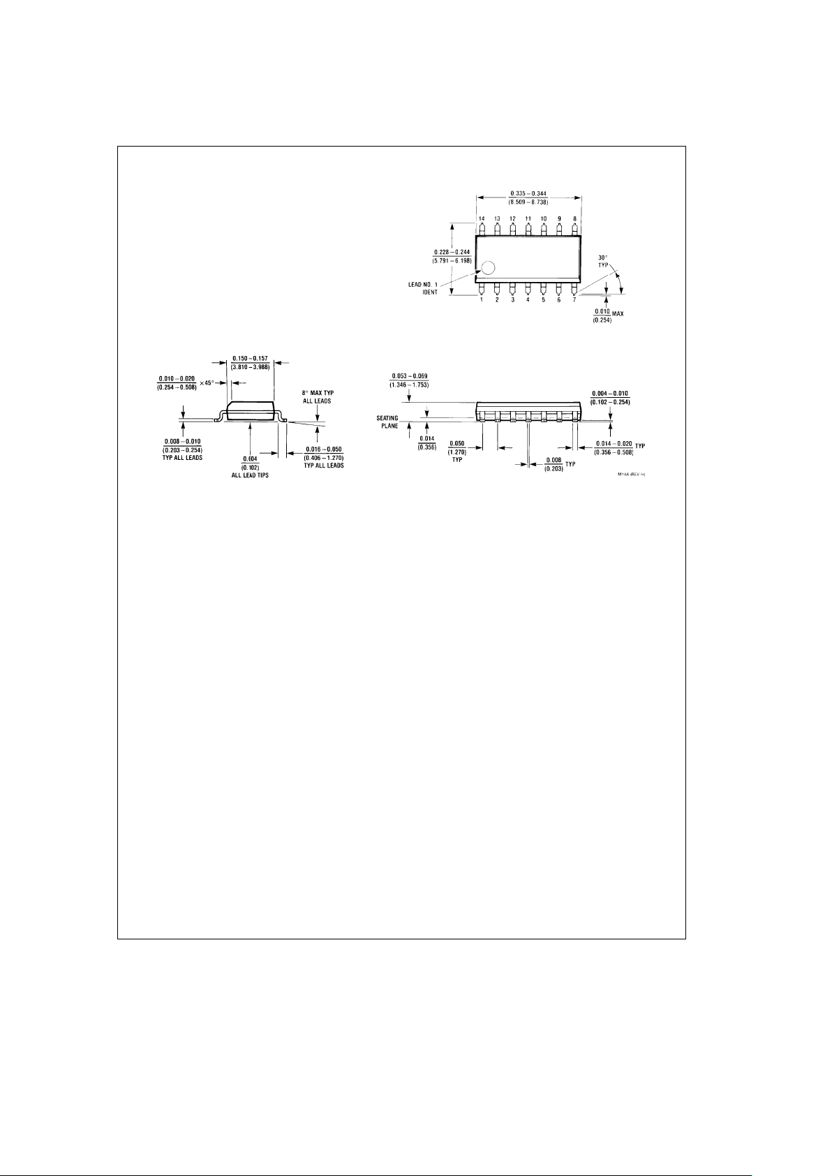
Physical Dimensions inches (millimeters)
14-Lead Small Outline Integrated Circuit
NS Package Number M14A
7
Page 8

CGS74B2525 1-to-8 Minimum Skew Clock Driver
Physical Dimensions inches (millimeters) (Continued)
14-Lead Plastic Dual-In-Line Package
NS Package Number N14A
LIFE SUPPORT POLICY
NATIONAL’S PRODUCTS ARE NOT AUTHORIZED FOR USE AS CRITICAL COMPONENTS IN LIFE SUPPORT
DEVICES OR SYSTEMS WITHOUT THE EXPRESS WRITTEN APPROVAL OF THE PRESIDENT OF NATIONAL
SEMICONDUCTOR CORPORATION. As used herein:
1. Life support devices or systems are devices or 2. A critical component is any component of a life
systems which, (a) are intended for surgical implant support device or system whose failure to perform can
into the body, or (b) support or sustain life, and whose be reasonably expected to cause the failure of the life
failure to perform, when properly used in accordance support device or system, or to affect its safety or
with instructions for use provided in the labeling, can effectiveness.
be reasonably expected to result in a significant injury
to the user.
National Semiconductor National Semiconductor National Semiconductor National Semiconductor
Corporation Europe Hong Kong Ltd. Japan Ltd.
1111 West Bardin Road Fax: (
a
49) 0-180-530 85 86 13th Floor, Straight Block, Tel: 81-043-299-2309
Arlington, TX 76017 Email: cnjwge@tevm2.nsc.com Ocean Centre, 5 Canton Rd. Fax: 81-043-299-2408
Tel: 1(800) 272-9959 Deutsch Tel: (
a
49) 0-180-530 85 85 Tsimshatsui, Kowloon
Fax: 1(800) 737-7018 English Tel: (
a
49) 0-180-532 78 32 Hong Kong
Fran3ais Tel: (
a
49) 0-180-532 93 58 Tel: (852) 2737-1600
Italiano Tel: (
a
49) 0-180-534 16 80 Fax: (852) 2736-9960
National does not assume any responsibility for use of any circuitry described, no circuit patent licenses are implied and National reserves the right at any time without notice to change said circuitry and specifications.
 Loading...