

Page 1
GaAs FET CFY 25
● Low noise
● High gain
● For front-end amplifiers
● lon-implanted planar structure
● All gold metallization
ESD: Electrostatic discharge sensitive device, observe handling precautions!
Type Ordering Code
Marking
(tape and reel)
CFY 25-17
CFY 25-20
CFY 25-23
C 5
C 6
C 7
Q62703-F106
Q62703-F107
Q62703-F108
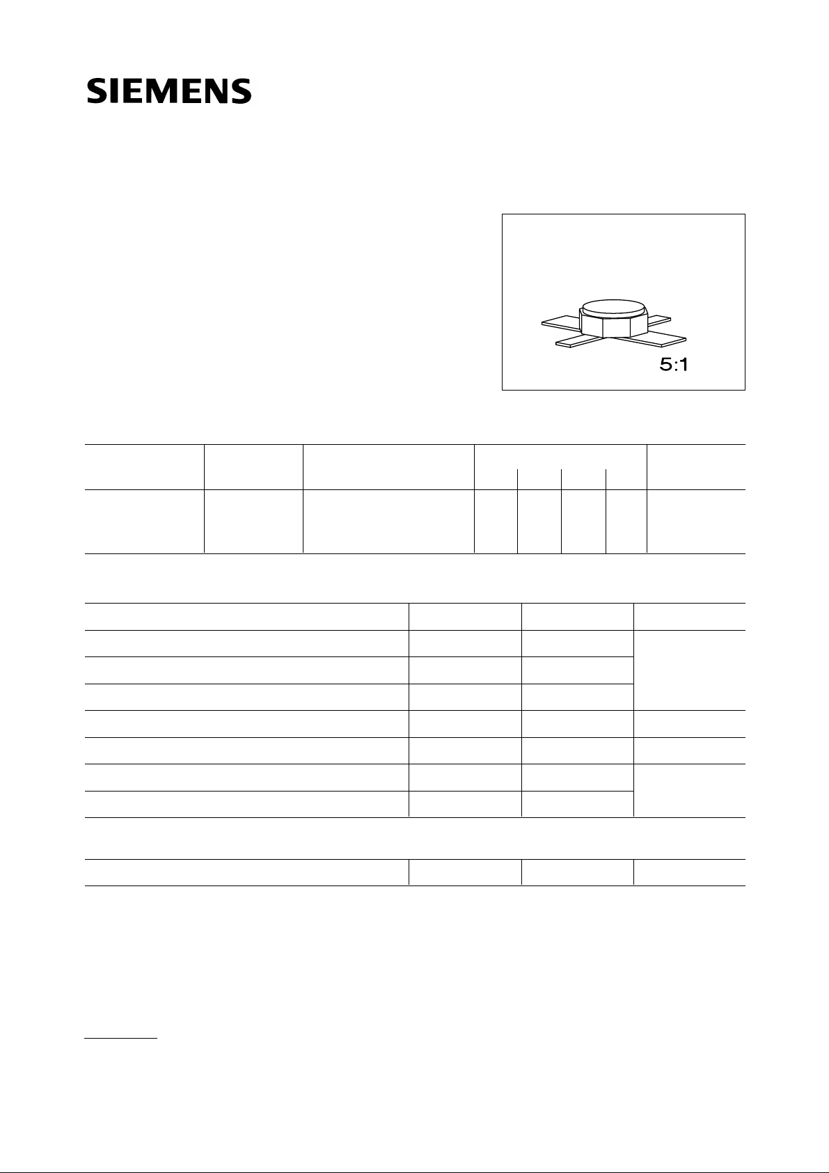
Pin Configuration
1 2 3
D S G
4
S
Package
Micro-X
Maximum Ratings
Parameter Symbol Values Unit
Drain-source voltage V
DS 5V
Drain-gate voltage VDG 7
Gate-source voltage V
GS – 5 … + 0
Drain current ID 80 mA
Total power dissipation, T
S ≤ 56 ˚C
2)
Ptot 250 mW
Channel temperature Tch 150 ˚C
Storage temperature range T
stg – 65 … + 150
1)
Thermal Resistance
Channel - soldering point
1)
For detailed information see chapter Package Outlines.
2)
TS is measured on the source lead at the soldering point to the pcb.
2)
Rth chS 375 K/W
Semiconductor Group 1
07.94
Page 2
Electrical Characteristics
A = 25 ˚C, unless otherwise specified.
at T
CFY 25
Parameter Symbol
I
DSS 15 30 60
DS = 3 V, VGS = 0
V
V
p – 0.3 – 1.0 – 3.0
ID = 1 mA, VDS = 3 V
I
G – 0.1 2
D = 15 mA, VDS = 3 V
I
g
m 30 40 –
D = 15 mA, VDS = 3 V
I
F
DS = 15 mA, VDS = 3 V, f= 12 GHz CFY25-17
I
CFY25-20
CFY25-23
Associated gain
DS = 15 mA, VDS = 3 V, f= 12 GHz CFY25-17
I
G
a
CFY25-20
CFY25-23
min. typ. max.
–
–
–
9
8.5
8.5
1.6
1.9
2.2
9.5
9
9
1.7
2.0
2.3
–
–
–
UnitValues
mADrain-source saturation current
VPinch-off voltage
µAGate leakage current
mSTransconductance
dBNoise figure
Semiconductor Group 2
Page 3

CFY 25
Total power dissipation Ptot = f (TS; TA*)
* Package mounted on alumina
Output characteristics ID = f (VDS)
Transfer characteristics I
DS = 3 V
V
D = f (VG)
Semiconductor Group 3
Page 4

Common Source Noise Parameters
Γ
f
Fmin Ga RN NF50 Ω
opt
CFY 25
r
N
G(F
50 Ω)
GHz dB dB MAG ANG Ω –dB
–
dB
ID = 15 mA, VDS = 3.0 V, Z0 = 50 Ω
2
4
6
8
10
12
14
0.60
0.77
1.00
1.25
1.55
1.77
2.15
18.5
14.6
12.4
11.0
9.8
9.0
8.1
0.70
0.59
0.50
0.47
0.45
0.43
0.41
31
63
103
140
174
– 156
– 130
29
21
13
7.3
5.6
7.1
18
0.580
0.420
0.260
0.146
0.112
0.142
0.360
0.10
0.14
0.19
0.23
0.28
0.29
0.46
2.0
1.8
1.8
2.0
2.4
2.5
3.0
11.4
10.5
9.3
8.2
7.3
6.4
5.8
Source impedance for min. noise figure
D = 15 mA, VDS = 3 V
I
Circles of constant noise figure
D = 15 mA, VDS = 3 V, f = 12 GHz
I
Semiconductor Group 4
Page 5

CFY 25
Minimum noise figure Fmin = f (f)
Associated gain G
D = 15 mA, VDS = 3 V, ZSopt
I
a = f (f)
Minimum noise figure Fmin = f (ID)
Associated gain G
DS = 3 V, f = 12 GHz, ZSopt
V
a = f (ID)
Semiconductor Group 5
Page 6

Common Source S Parameters
CFY 25
fS
11 S21 S12 S22
GHz MAG ANG MAG ANG MAG ANG MAG ANG
ID = 15 mA, VDS = 3 V, Z0 = 50 Ω
1.0
2.0
3.0
4.0
5.0
6.0
7.0
8.0
9.0
10.0
11.0
12.0
13.0
14.0
15.0
16.0
17.0
18.0
0.99
0.96
0.91
0.86
0.81
0.77
0.74
0.70
0.68
0.67
0.67
0.66
0.66
0.66
0.66
0.66
0.66
0.66
– 21
– 42
– 67
– 87
– 107
– 125
– 145
– 165
178
161
146
132
117
103
90
77
63
47
3.83
3.73
3.55
3.34
3.10
2.92
2.74
2.57
2.42
2.31
2.20
2.10
2.02
1.94
1.90
1.84
1.80
1.78
161
141
121
103
86
70
54
37
23
– 4
– 17
– 31
– 44
– 57
– 70
– 84
– 99
0.026
0.049
0.069
0.083
0.093
0.100
0.105
0.107
0.108
9
0.109
0.110
0.110
0.110
0.112
0.115
0.119
0.125
0.132
75
61
45
33
21
11
– 9
– 17
– 24
– 30
– 36
– 42
– 49
– 55
– 63
– 72
– 83
0.68
0.66
0.63
0.59
0.56
0.52
1
0.48
0.45
0.42
0.41
0.39
0.37
0.36
0.35
0.34
0.33
0.32
0.31
– 13
– 27
– 41
– 55
– 66
– 77
– 89
– 102
– 112
– 124
– 134
– 145
– 158
– 169
180
165
151
136
S11, S22
ID = 15 mA, VDS = 3 V, Z0 = 50 Ω
S12, S21
ID = 15 mA, VDS = 3 V, Z0 = 50 Ω
Semiconductor Group 6
 Loading...