

Page 1
µ m × 90 µ
SM8223A
NIPPON PRECISION CIRCUITS INC.
FSK Decoder and DTMF Receiver IC
OVERVIEW
The SM8223A is a FSK (Frequency shift keying) decoder and DTMF (Dual tone multi-frequency) receiver IC.
It is fabricated using a CMOS process and features a power-down function for low power dissipation operation. The FSK decoder and DTMF receiver have the same performance characteristics as dedicated ICs that
perform the same functions, with the added benefit of an FSK decoder/DTMF receiver auto-select function
using the telephone tip/ring input signal. It also features a ring (call signal) signal detection circuit, making for
easy construction of low power dissipation, high-performance analog telephone-related applications.
FEATURES
■
Both FSK signal caller-ID information services
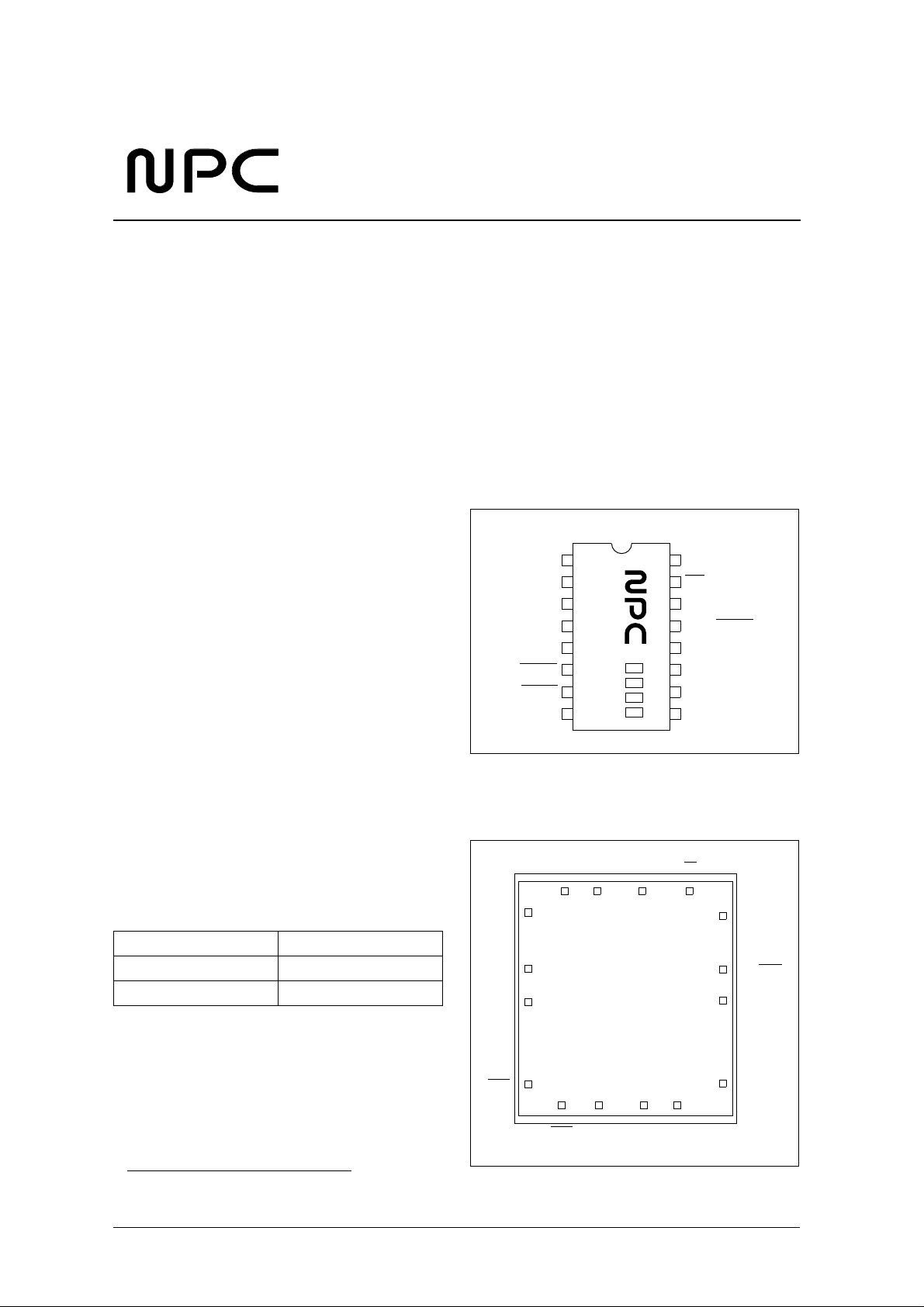
PINOUT
(Top view)
and DTMF signal caller-ID information services
supported
■
FSK decoder/DTMF receiver auto-select function
■
Ring (call signal) signal detection circuit built-in
■
Serial I/O
■
Input gain adjustment circuit built-in
■
Power-down mode
■
Single supply operation: 3.0V ± 10%
■
3.579545MHz external crystal oscillator frequency
■
Molybdenum-gate CMOS process
TIP
RING
GS
AGND
RDIN
RDRC
RDET
PDWN
1
SM8223AP
8
16
9
VDD
DV
DOUT
FSK/DTMF
IC
OSCIN
OSCOUT
GND
APPLICATIONS
1
■
Telephones, fax machines and modems that support caller-ID information services
■
Adapters for caller-ID information service functions
■
Telephones, fax machines and modems that support remote operation functions
ORDERING INFORMATION
De vice Pack ag e
SM8223A 16-pin DIP
CF8223A Chip
PINOUT
(Unit: µ m)
GS
AGND
RDIN
RDRC
(0, 0)
RING TIP VDD DV
PDWN GND OSCOUT
RDET
Pad size : 9 0
m
1. Auto-select function operates if the FSK signal conforms to the Bellcore GR-30-CORE standard.
(2810, 3160)
DOUT
FSK/DTMF
IC
OSCIN
NIPPON PRECISION CIRCUITS—1
Page 2
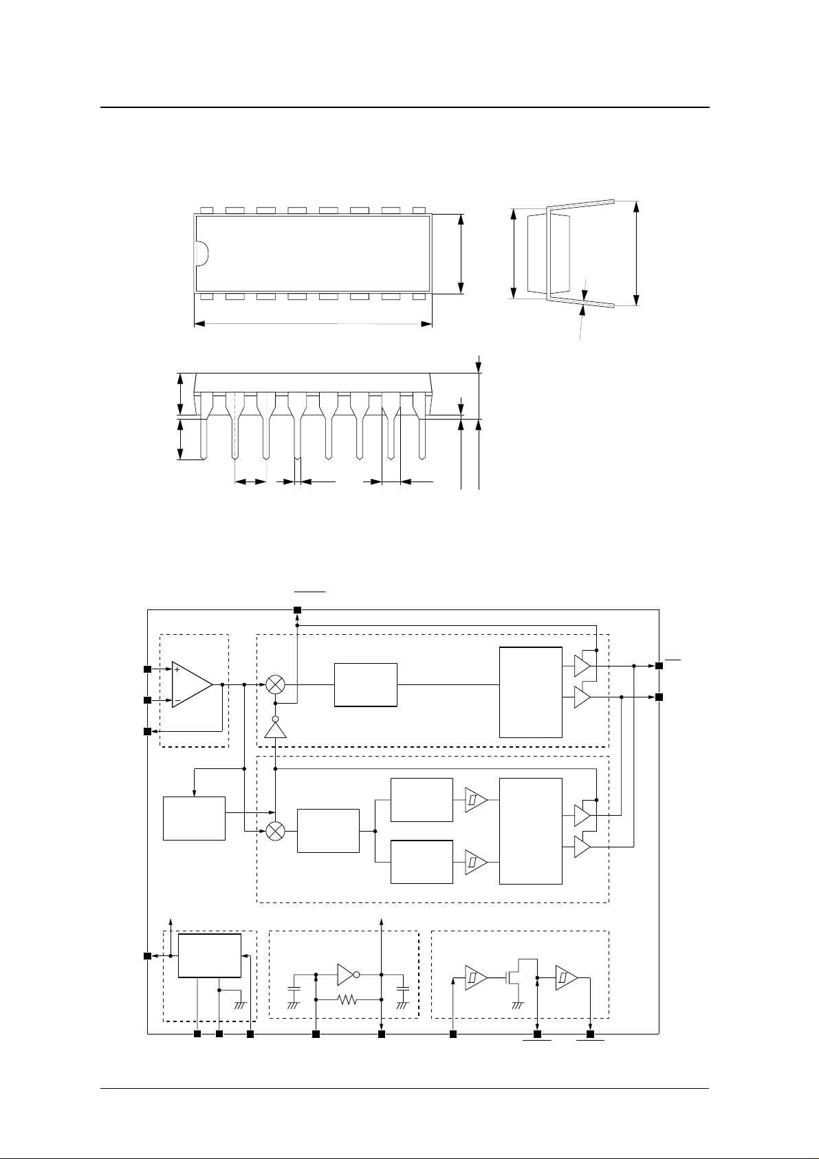
PACKAGE DIMENSIONS
(Unit: mm)
19.05
SM8223A
6.35
7.49 to 8.13
8.13 to 9.40
0.25
3.18 3.30
BLOCK DIAGRAM
Differential
Amplifier
TIP
RING
GS
FSK/DTMF
Discriminator
Logic
2.54
2.54 0.46 1.52
FSK/DTMF
FSK Decoder
Band Pass
Filter
High Group
Filter
Dial Tone
Filter
Low Group
Filter
3.68 to 4.32
0.38 to 1.02
FSK
Decoder
Logic
DTMF
Decoder
Logic
DV
DOUT
AGND
Bias
Circuit
GNDVDD PDWN
DTMF Receiver
OSC Ring Detect
OSCIN OSCOUT RDIN
RDRC RDET
NIPPON PRECISION CIRCUITS—2
Page 3
µ
PIN DESCRIPTION
SM8223A
Number Name I/O Function
1 TIP I Tip input. Connected to the telephone line through a protection circuit 1046 2934
2 RING I Ring input. Connected to the telephone line through a protection circuit 63 8 2934
3GSO
4 AG N D O Analog ground output. Inter nal reference voltage (V
5 RDIN I
6 RDRC
7 RDET
8PDWNI
9 G ND – Ground. Connected to the system ground potential. 1634 226
10 OSCOUT O
11 OSCIN I
12 I C I Test input. Tied LOW for normal operation. 2634 1550
13 FSK/DTMF
14 DOUT O
15 D
16 V D D – Supply 1612 2934
V O Data trigger output. Data is output on DOUT when this pin goes LOW. 2211 2934
Input-stage amplifier gain-select output. Used to adjust the gain of the inputstage amplifier.
/2) output level 17 6 1954
DD
Ring detector input. Used for line reversal and ring signal detection.
Connected for ring detection of attenuated ring signals.
Ring detector RC terminal. Connected to an RC network which sets the ring
I/O
detector delay time.
Ring detector output. RDRC
O
output when ring signal is detected.
Pow er-down control input. LOW-level for normal operation. HIGH-level for
pow er-down state. In the pow er-down state, pins AGND, OSCOUT, DOUT,
and DV are HIGH.
Cr ystal oscillator output. The cr ystal oscillator element is connected between
this pin and OSCIN.
Crystal oscillator input. The crystal oscillator element is connected between
this pin and OSCOUT.
FSK/DTMF discriminator output. HIGH-level output when receiving FSK
O
signal, and LOW -level output when receiving DTMF signal.
Demodulator output. Demodulated FSK or DTMF signal output. HIGH-level
output in pow er-down state.
-input Schmitt-trigger buffer output. L OW -level
Pad dimensions (
XY
176 2665
176 1534
176 492
596 226
1063 226
2053 226
2634 506
2634 1942
2634 2623
m)
NIPPON PRECISION CIRCUITS—3
Page 4
−
−
−
° C
∆
−
−
° C
SM8223A
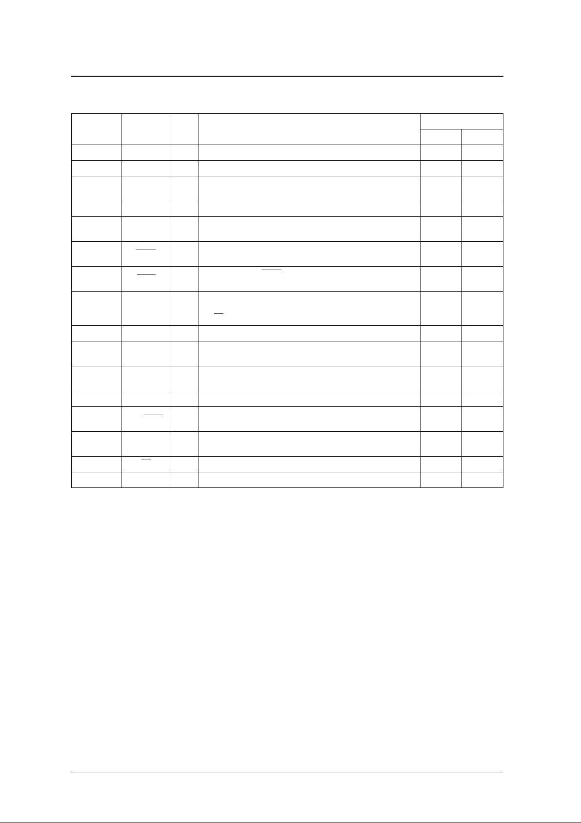
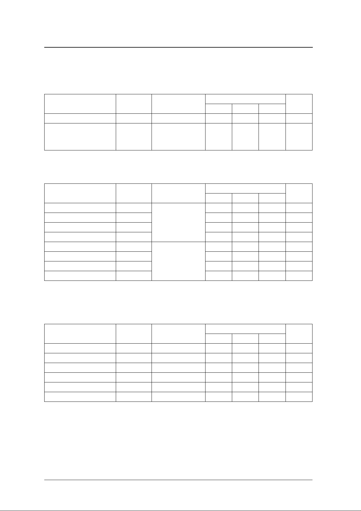
SPECIFICATIONS
Absolute Maximum Ratings
GND = 0V
Parameter Symbol Rating Unit
Supply voltage range V
Input voltage range V
DC input current I
Storage temperature range T
Recommended Operating Conditions
GND = 0V
−
−
DD
IN
IN
stg
0.5 to 5.0 V
0.3 to V
+ 0.3 V
DD
±10 m A
40 to 125
Parameter Symbol Condition
Supply voltage V
Clock frequency f
Clock frequency accuracy
Operating temperature T
DC Electrical Characteristics
V
= 3.0V ± 0.3V, GND = 0V, f
DD
Parameter Symbol Condition
Supply current consumption I
Power-down state current I
PD WN, RDIN, RDRC LOW -level
input voltage
PD WN, RDIN, RDRC
HIGH-level
input voltage
OSCIN LOW-level input voltage V
OSCIN HIGH-level input voltage V
DOUT, DV, RDET, FSK/DTMF LOW -
level output current
V, RDET, FSK/DTMF HIGH-
DOUT, D
level output current
P DWN, RDIN input leakage current I
RDRC output leakage current I
CLK
DPD
V
V
I
DD
CLK
f
C
a
= 3.579545MHz, T
P DW N = 0V, RDIN = 0V,
DD
IL1
IH1
IL2
IH2
I
OL
OH
IN
OFF
RDRC = 0V, all other inputs
open
PDWN = V
RDRC = 0V, all other inputs
open
When external clock input – – 0.3V
When external clock input 0.7V
Rating
min typ max
2.7 – 3.3 V
– 3.579545 – MH z
0.1 – +0.1 %
20 – 85
= − 20 to 85 ° C unless otherwise noted.
a
Rating
min typ max
– – 4.5 mA
, RDIN = 0V,
DD
––15µA
– – 0.3V
0.7V
DD
DD
––V
––V
2––mA
––
1– 1µA
––1µA
Unit
Unit
DD
DD
0.8 m A
V
V
NIPPON PRECISION CIRCUITS—4
Page 5
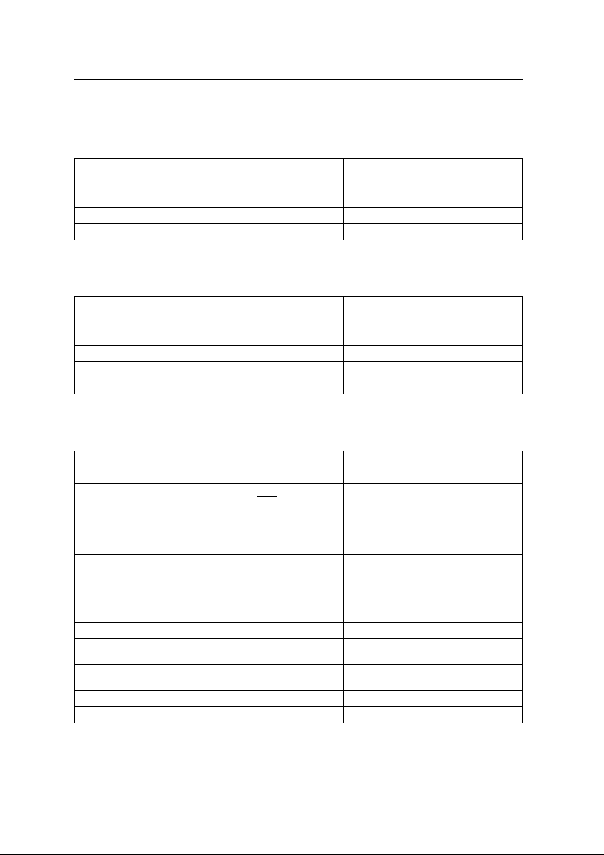
AC Electrical Characteristics
FSK decoder
V
= 3.0V ± 0.3V, GND = 0V, f
DD
CLK
SM8223A
= 3.579545MHz, T
− 40 −
−
−
Ω
= − 20 to 85 ° C unless otherwise noted.
a
Parameter Symbol Condition
Detection sensitivity Typical application circuit
Ma rk signal and SPACE
Noise reduction ratio
signal are same level.
Noise: Random noise from
200Hz to 3400Hz.
min typ max
20 – – d B
Rating
Unit
37.5 0 d B m
DTMF receiver
V
= 3.0V ± 0.3V, GND = 0V, f
DD
Parameter Symbol Condition
Detection frequency deviation
Non-detection frequency deviation ±3.5 – – %
Detection sensitivity
Non-detection sensitivity ––
Signal level error
High-frequency rejection ratio – 1 8 – d B
Noise rejection ratio –12–dB
Dial tone rejection ratio –20–dB
1. Input signal is up to V
DD
level.
= 3.579545MHz, T
CLK
Typical application circuit
Typical application circuit
= − 20 to 85 ° C unless otherwise noted.
a
Rating
min typ max
±1.5% ± 2 – – Hz
32.0 – 0.0 dB m
50.0 dB m
––6dB
1
Unit
Input-stage amplifier Characteristics
V
= 3.0V ± 0.3V, GND = 0V, f
DD
Parameter Symbol Condition
Input leakage current I
Input resistance R
DC open-loop voltage gain A
Unity gain frequency f
Load capacitance C
Load resistance R
= 3.579545MHz, T
CLK
IN
IN
VOL
C
L
L
= − 20 to 85 ° C unless otherwise noted.
a
Rating
min typ max
––1µA
–1–M
30 – – d B
80 – – kHz
– – 100 pF
50 – – k Ω
Unit
NIPPON PRECISION CIRCUITS—5
Page 6

Timing Characteristics
Oscillator
V
= 3.0V ± 0.3V, GND = 0V, T
DD
SM8223A
= − 20 to 85 ° C unless otherwise noted.
a
µ
Parameter Symbol Condition
Clock HIGH-level pulsewidth t
Clock LOW -level pulsewidth t
Clock rise time t
Clock fall time t
FSK decoder
V
= 3.0V ± 0.3V, GND = 0V, f
DD
Parameter Symbol Condition
Pow er-down release time t
Oscillator start-up time t
Ma rk signal to DV ON time t
FSK flag setup time t
FSK flag hold time t
Input to DOUT delay time t
DOUT rise time t
DOUT fall time t
DOUT data rate t
WH
WL
r
f
= 3.579545MHz, T
CLK
DPD
DOSC
DED
AF
AH
ADD
Dr0
Df0
DWL/H
DV = LOW – – 3.75 ms
Rating
min typ max
110 – – ns
110 – – ns
––30ns
––30ns
= − 20 to 85 ° C unless otherwise noted.
a
Rating
min typ max
–8–ms
–5–ms
––
833
(1/1.2kHz)
––10ns
–15ms
––20ns
––20ns
1188 1200 1212 baud
Unit
Unit
s
DTMF receiver
V
= 3.0V ± 0.3V, GND = 0V, f
DD
Parameter Symbol Condition
DOUT, DV rise time t
DOUT, DV fall time t
Signal detection time t
Received signal non-detection time t
Pause detection time t
Pause non-detection time t
DV output data delay time t
Pow er-down release time t
Oscillator start-up time t
DOUT data rate t
DTMF flag setup time t
= 3.579545MHz, T
CLK
Dr0
Df0
RE
RE
PA
PR
BDD
DPD
DOSC
DWL/H
AF
DV ––45ms
DV 20 – – ms
DV ––25ms
DV 20 – – ms
= − 20 to 85 ° C unless otherwise noted.
a
Rating
min typ max
––20ns
––20ns
––5ms
–8–ms
–5–ms
1188 1200 1212 baud
––
833
(1/1.2kHz)
Unit
µ
s
NIPPON PRECISION CIRCUITS—6
Page 7

OSCIN input timing (when external input)
VDD
OSCIN
VSS
tf tr
FSK receive timing (1)
SM8223A
tWL tWH
Tip/Ring
RDET
DV
FSK/DTMF
DOUT
PDWN
1st Ring
Ch. seizure Mark Data packet
1010101... 111...
tDED
tAF tHF
tADD
tDPD
tDOSC
Data
Data
2nd Ring
Data output has
no Ch.seizure signal.
OSCOUT
FSK receive timing (2)
Tip/Ring
DOUT
LSBStart bit
0 b0 b1 b2 b3 b4 b5 b6 b7 1 0 b0 b1b6 b7 1
MSB Stop bit
tADD
b4 b5 b6 b7 b0 b1 b2 b3 b4 b5 b6 b7 b0 b1
1010
NIPPON PRECISION CIRCUITS—7
Page 8

DTMF receive timing (1)
SM8223A
tPR tREtPA
DTMF Data #1 #1Tip/Ring
tRE
DV
FSK/DTMF
DOUT
tDPD
PDWN
tDOSC
OSCOUT
DTMF receive timing (2)
tAF
tBDD
Data #1
DTMF Data #2
Data #2
DV
DOUT
(FSK/DTMF) DOUT output timing
DOUT
tDf0 tDr0
tBDD
Q1 Q2 Q3 S0
Start bit
DTMF data Checksum
tDWL tDWH
(2'mod16)
S3S2S1Q0
Stop bit
10
90%
10%
NIPPON PRECISION CIRCUITS—8
Page 9

SM8223A
FUNCTIONAL DESCRIPTION
Ring Signal Detector
The telephone tip and ring signals pass through a
protection circuit and are input to a resistor, capacitor and diode bridge network, shown in figure 1.
a
c
TIP
RING
C2
C2
R3
R3
Db
Figure 1. Ring signal detector circuit
The diode bridge full-wave rectified output signal
(point a) is reduced in level by a resistor voltage
divider comprising R1 and R2 (point b), and then
input on RDIN. When the ring signal input on RDIN
exceeds the Schmitt buffer trigger voltage (0.7VDD),
the output switches the open-drain RDRC pin. The
signal at RDRC (point c) drives a time-constant cir-
R1
b
RDIN
RDRC
RDET
d
D1
R2
R4
C1
cuit comprised by resistor R4 and capacitor C1 connected to the input of a second Schmitt buffer to
generate the detector signal output on RDET (point
d). Thus, RDET goes LOW when the ring or tip signal exceeds the level set by the resistor voltage
divider.
NIPPON PRECISION CIRCUITS—9
Page 10

SM8223A
VRIG
VDD
VSS
Point a Signal
VDD
VSS
Point b Signal
VDD
VSS
Point c Signal
VDD
VSS
Point d Signal
Figure 2. Ring signal detector circuit waveform transitions
The voltage divider level and RC time constant are
given by the following equations, respectively.
0.7VDD
0.3VDD
VRIG
0.7VDD
0.3VDD
0.7VDD
0.3VDD
0.7VDD
0.3VDD
R
1
0.7V
C1R
4
--------------------------------
DD
R1R2R
++
t
-------------------------------------=
V
DD
------------------------- -
In
V
–
DDVT
V
⋅=
RIG
3
where t is the guard time, and the trigger level satisfies the expression 0.3VDD ≤ VT ≤ 0.7VDD.
NIPPON PRECISION CIRCUITS—10
Page 11

Input Differential Amplifier
SM8223A
The SM8223A uses an input differential amplifier
for input gain adjustment of the tip/ring signal input
to the FSK detector or DTMF receiver. Differential
input configuration and single-ended input configu-
R1C1
R1C1
R3
R4
TIP
RING
R2
GS
AGND
C
Differntial Input
Figure 3. Input circuits
The gain for single-ended configurations is given by
the following equation.
ration circuits are shown in figure 3. A bypass capacitor should be connected between GND and AGND
in both circuit configurations.
TIP
R1C1
C
R2
RING
GS
AGND
Single-Ended Input
and the input impedance is given by the following
equation.
R
A
2
------=
V
R
1
The gain for differential configurations is given by
the following equation,
R
2
------
A
V
where R
R
1
R2R
4
-------------------==
3
R2R4+
FSK/DTMF Auto-discriminator
The SM8223A examines the tip/ring input signal and
determines the nature of the signal, FSK or DTMF,
and invokes the corresponding circuits, FSK decoder
or DTMF receiver, respectively. It determines
whether the input signal is an FSK signal or DTMF
Zi2 R
2
+=
1
2
1
-----------
ωC
1
signal by the presence or otherwise of the channel
seizure information in the FSK signal header. This
function automatically discriminates between the
input signals if the FSK signal conforms to the
Bellcore GR-30-CORE standard.
NIPPON PRECISION CIRCUITS—11
Page 12

FSK Demodulator
SM8223A
When an FSK signal is received, the FSK/DTMF
signal discriminator circuit sets the FSK/DTMF pin
HIGH and connects the input signal to the FSK
demodulator circuit. Demodulated data is output on
DOUT with the format shown in figure 4. The FSK
signal conforms to the following Bellcore standard.
LSBStart bit
FSK signal
DOUT
b4 b5 b6 b7 b0 b1 b2 b3 b4 b5 b6 b7 b0 b1
0 b0 b1 b2 b3 b4 b5 b6 b7 1 0 b0 b1b6 b7 1
Figure 4. FSK signal to DOUT output
Table 1. FSK signal
Parameter Description
Modulation type
Logic “1” data (mark) 1200 ± 12 Hz
Logic “0” data (space) 2200 ± 22 Hz
Signal level (mark)
Signal level (space)−36 to −12 dBm
Data transfer rate 1200 ± 12 baud
MSB Stop bit
Continuous-phase binary frequency-shiftkeying
−
32 to −12 dBm
1010
DTMF Demodulator
When a DTMF signal is received, the FSK/DTMF
signal discriminator circuit sets the FSK/DTMF pin
LOW and connects the input signal to the DTMF
demodulator circuit. The DTMF signal is comprised
by a high-group frequency and a low-group frequency which, in combination, represent a point in
the DTMF matrix.
Table 2. DTMF matrix
Low group
697Hz 123A
770Hz 456B
852Hz 789C
941Hz *0#D
1209Hz 1336Hz 1477Hz 1633Hz
The DTMF receiver demodulates the received
DTMF signal and outputs data bits Q0 to Q3 and a 4bit (2-mod-16) checksum S0 to S3 in serial format on
DOUT.
High group
Table 3. DTMF signal output (DOUT)
Matrix
input
1 10001111
2 01000111
3 11001011
4 00100011
5 10101101
6 01100101
7 11101001
8 00010001
9 10011110
0 01010110
* 11011010
# 00110010
A 10111100
B 01110100
C 11111000
D 00000000
DTMF Checksum
D
0D1
Q0Q1Q2Q3S0S1S2S
D2D3D4D5D6D
7
3
NIPPON PRECISION CIRCUITS—12
Page 13

SM8223A
DTMF signal
DOUT
DTMF DATA
Start bit
Figure 5. DTMF signal to DOUT output
The DTMF receiver determines whether the received
data (DTMF signal) is valid after an interval of
t
≥ 40ms stable reception. If valid, DV goes
REC
LOW and data is output on DOUT. If DTMF data is
not detected after an interval t
≥ 20ms, a data
SPA
pause is activated and the next DTMF signal is in a
S3S2S
Q
0
Q1Q2Q3S
DTMF data
(LSB first)
1
0
Checksum
(2'mod16)
(LSB first)
10
Stop bit
wait state (see timing diagrams in AC Electrical
Characteristics). The SM8223A DTMF receiver can
be used as a general-purpose DTMF receiver without
the need for the external time constant circuit, in
which case the resistor/capacitor/diode network can
be omitted.
NIPPON PRECISION CIRCUITS—13
Page 14

TYPICAL APPLICATION CIRCUIT
D1
D1
D1
D1
R2
R2
D2
TIP
RING
VS
C3
R1C1
R1C1
R6
D2
R4
D1
R7
SM8223A
R5
C2
R9
R3
TIP
RING
GS
AGND
RDIN
RDRC
RDET
PDWN
VDD
DV
DOUT
FSK/
DTMF
OSCIN
OSCOUT
GND
C5
IC
X'tal
C3
R6
Symbol Rating Unit
1
R
1
1
R
2
1
R
3
1
R
4
1
R
5
D
1
C
1
C
2
2
R
6
2
R
7
2
R
8
2
R
9
C
3
2
C
4
D
2
C
5
240 kΩ
34 kΩ
464 kΩ
53.6 kΩ
60.4 kΩ
1N4003 –
22 nF
0.1 µF
430 kΩ
270 kΩ
27 kΩ
270 kΩ
22 nF
470 nF
1N4004 –
0.1 µF
VS – –
X’tal 3.579545 MH z
1. Ref er to the Input Differential Amplifier.
2. Refer to the Ring Signal Detector.
D2
D2
R8
C4
NIPPON PRECISION CIRCUITS—14
Page 15

SM8223A
NIPPON PRECISION CIRCUITS INC. reserves the right to make changes to the products described in this data sheet in order to
improve the design or performance and to supply the best possible products. Nippon Precision Circuits Inc. assumes no responsibility for
the use of any circuits shown in this data sheet, conveys no license under any patent or other rights, and makes no claim that the circuits
are free from patent infringement. Applications for any devices shown in this data sheet are for illustration only and Nippon Precision
Circuits Inc. makes no claim or warranty that such applications will be suitable for the use specified without further testing or modification.
The products described in this data sheet are not intended to use for the apparatus which influence human lives due to the failure or
malfunction of the products. Customers are requested to comply with applicable laws and regulations in effect now and hereinafter,
including compliance with export controls on the distribution or dissemination of the products. Customers shall not export, directly or
indirectly, any products without first obtaining required licenses and approvals from appropriate government agencies.
NIPPON PRECISION CIRCUITS INC.
4-3, Fukuzumi 2-chome
Koto-ku, Tokyo 135-8430, Japan
NIPPON PRECISION CIRCUITS INC.
Telephone: 03-3642-6661
Facsimile: 03-3642-6698
NC9909AE 2000.02
NIPPON PRECISION CIRCUITS—15
 Loading...