

Page 1
CF5760 series
NIPPON PRECISION CIRCUITS INC.
CMOS Analog Clock IC
OVERVIEW
The CF5760 series devices are analog clock ICs that derive their timing from a 32.768 kHz oscillator element.
They feature a reset function (optional seconds control function) which can be used to maintain accurate time.
Various alarm functions and motor outputs are available to match a wide range of clock specifications.
FEATURES
■
1.2 to 2.0V operating supply voltage
■
1.2µA (typ) / 1.5V current consumption
■
32.768 kHz oscillator circuit
■
Oscillator capacitance C
■
Alarm output function
■
Reset function (optional seconds control function)
■
Input chattering elimination function (AI/R)
■
Chip form (CF5760 ×× )
and C
G
built-in
D
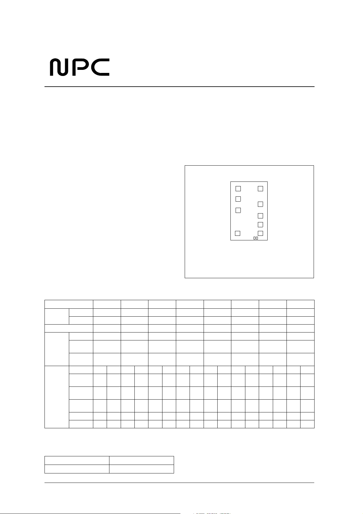
PAD LAYOUT
VDD
AI/R
O1
O2
(0,0)
Top view
1
XT
9
2
8
XTN
3
7
AON
6
AO
45
HA5760
VSS
Chip size: 0.76
×
1.21 mm
Chip thickness: 300 ± 30 µm
Pad size: 100
Re verse side: V
×
100 µm
level
DD
SERIES CONFIGURATION
CF5760AA CF5760BA CF5760CC CF5760DA CF5760EA CF5760FC CF5760HA CF5760JA
C
(pF) 33333333
Built-in
capacitance
Alarm input/reset input level HIGH/LOW HIGH/LOW LOW/HIGH LOW/HIGH –/LOW LOW /HIGH LOW/HIGH LOW/HIGH
Motor output
Alarm output
1. Built-in capacitance includes the parasitic capacitance.
G
1
C
(pF) 25 25 33 25 25 33 25 25
D
Active level LOW LOW HI GH LOW – – HI GH –
Needle period
t
(s)
CY
Pulsewidth
(ms)
t
PW
Pins AO AO N AO AON AO AO N A O AO N AO AON AO AO N A O AO N AO AON
Active level HI GH LOW HI GH
Frequency
(kHz)
f
PW
Modulation
(Hz)
f
CY
I
min (
µ
A) 900 900 900 10 900 900 900 10 – – 900 900 900 900 900 10
OH
I
min (
µ
A) 900 900 10 10 900 900 10 10 – – 900 900 900 900 10 10
OL
111110.0625 1 0.0625
23.4 23.4 31.25 27.3 1000 62.5 46.875 62.5
F
HIGH LOW HIGH
(32kHz)
44DC–22DC–––2222DC–
88––8 + 18 + 1––––8 + 18 + 18 + 18 + 1––
F
– – HIGH LOW HIGH LOW HIGH
(32kHz)
(32kHz)
F
ORDERING INFORMATION
De vice Pack ag e
CF5760
××
Chip form
NIPPON PRECISION CIRCUITS—1
Page 2
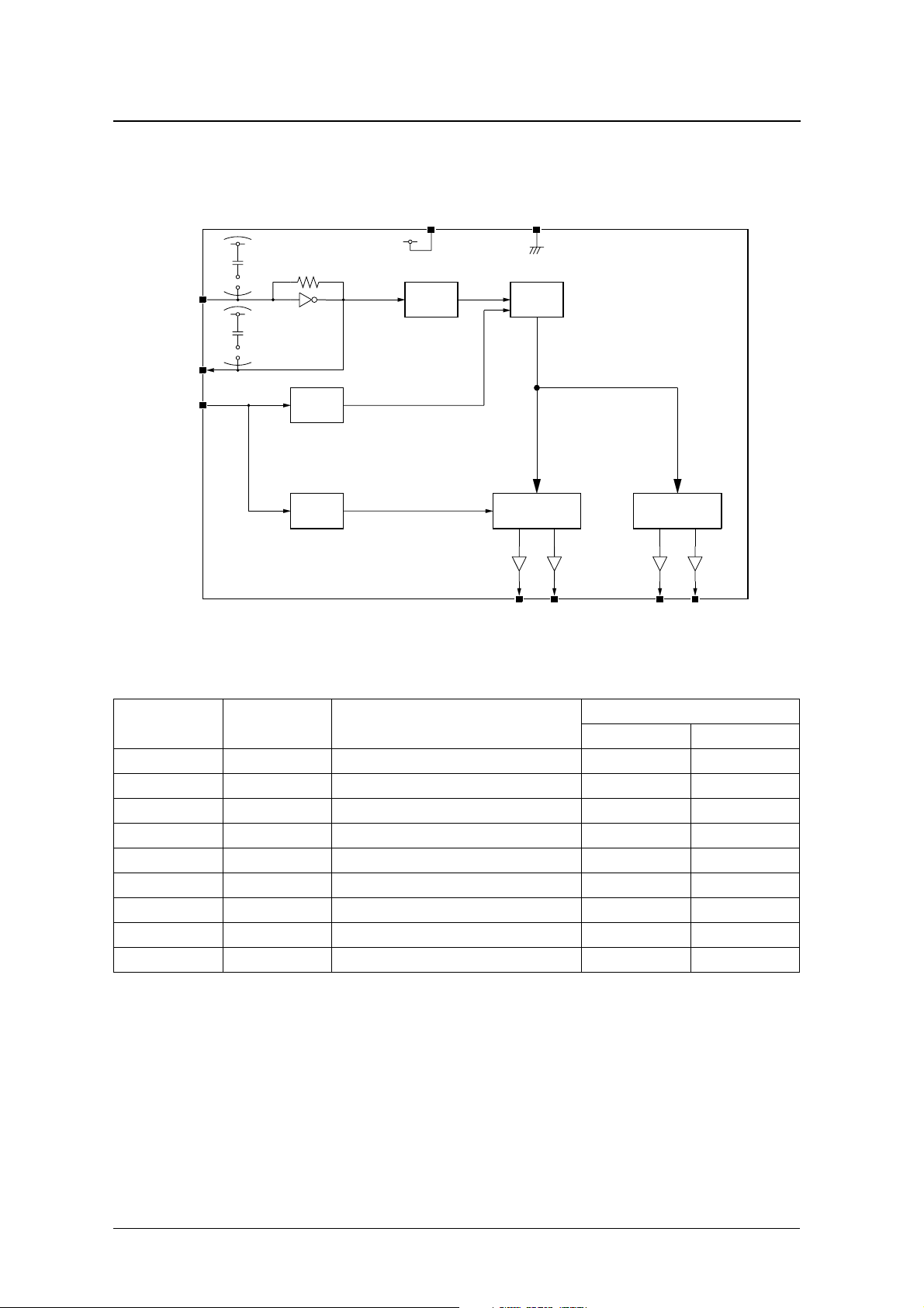
BLOCK DIAGRAM
CF5760 series
XT
XTN
AI/R
CG
CD
Reset
Input
Alarm
Input
VDD
7 Stage
Divider
VSS
9 Stage
Divider
Alarm Output
Control
AO AON
Motor Output
Control
O1 O2
PAD DESCRIPTION/DIMENSIONS
No. Name Description
1 VD D Supply 155 1065
2 AI/R Alarm input and reset input 15 5 85 4
3 O1 Motor output 1 155 6 20
4 O2 Motor output 2 145 1 45
5 V SS Ground 615 145
6 AO Alarm o utput 1 615 3 25
7 AON Alarm ou tput 2 615 50 5
8 XT N Oscillator output 61 5 74 6
9 X T Oscillator input 6 1 5 1065
Dimensions (µm)
XY
NIPPON PRECISION CIRCUITS—2
Page 3

SPECIFICATIONS
Absolute Maximum Ratings
Parameter Symbol Condition Rating Unit
Supply voltage range V
Input voltage range V
Ope rating temperature range T
Storage temperature range T
Electrical Characteristics
T
= 25 ° C, V
a
erwise noted
= 1.5V, V
DD
SS
DD
= 0V, C
−
V
IN
opr
stg
= 23pF, C
G
SS
C
CF5760 series
−
0.3 to 5.0 V
V
≤
V
≤
= 25pF, X’tal (f
D
SS
−
−
65 to 150
= 32.768kHz, C
0
V
IN
DD
30 to 80
= 50k Ω max) unless oth-
I
V
°
C
°
Parameter Symbol Condition
Ope r ating voltage V
Current consumption I
Oscillator start-up time t
Motor output current I
AI/R HIGH-level input current I
AI/R LOW -level input current I
Oscillator frequency stability
Alarm L O W-level output current
2
(AO, AON)
Alarm HIGH-level output current
2
(AO, AON)
F output voltage
Internal capacitance
1. R
is the load resistance connected between O1 and O2.
L
2. CF5760AA/ CC/ FC/ HA: If the outputs (AO or AON) are shor t circuit, the output current is I
3
4
3. The F output voltage rating, V F, when a load capacitance, C
ag e, 0.5V
4. C
G
, and the peak voltage.
DD
is the capacitance between VDD and XT. C
DD
DD
STA
MOT
IH
IL
∆
f/f V
I
OL1
I
OL2
I
OH1
I
OH2
V
F
C
G
C
D
D
O1 = O2 = open – 1.2 4.0 µA
V
= 1.2V – – 5.0 s
DD
V
= 1.2V, R
DD
V
= 1.5V 2 4 8 µ A
DD
V
= 1.5V 2 4 8 µ A
DD
= 1.2 to 2.0V – 0.5 1 .0 ppm/0.1V
DD
V
= 1.5V, V
DD
V
= 1.5V, V
DD
V
= 1.5V, V
DD
V
= 1.5V, V
DD
V
= 1.2V, C
DD
, is connected between pin F and VS S, is the differ en c e voltage between the center volt-
L
1
= 200
Ω
L
= 0.75V 900 2000 – µA
OL
= 0.75V 10 30 – µA
OL
= 0.75V 900 2000 – µ A
OH
= 0.75V 1 0 30 – µA
OH
= 50pF 0.4 – – V
L
is the capacitance between VDD and XTN.
AO
Rating
min typ max
1.2 – 2.0 V
4.0 – – mA
Refer to the SERIES LINEUP
≥
900
µ
A.
Unit
pF
pF
NIPPON PRECISION CIRCUITS—3
Page 4

CF5760 series
FUNCTIONAL DESCRIPTION
Motor Output
Motor output waveform (step motor driver)
tPW
O1
(Active High)
O2
(Active High)
tCY
tPW
tCY
tCY : Needle period
tPW : Pulse width
Motor output waveform (sweep motor driver)
tPW
62.5ms
O1
tCY
62.5ms
O2
tCY
62.5ms
tPW
62.5ms
tCY : Needle period
tPW : Pulse width
Input Chattering Elimination Function (AI/R)
A bounce delay is provided on the AI/R input to eliminate erroneous operation caused by input bounce (chattering).
t
ON
AI/R
(Active Low)
t
< 62.5ms: input is ignored.
ON
62.5
≤
t
≤
125ms: indeter minate
ON
t
> 125ms: input is accepted.
ON
Input Control Functions
When AI/R is open circuit, a 256Hz signal is output.
When AI/R is HIGH or LOW, it selects the alarm (HIGH)/reset (LOW) function or reset (HIGH)/alarm (LOW)
function depending on the version.
NIPPON PRECISION CIRCUITS—4
Page 5

CF5760 series
Reset Function (optional seconds control function)
When AI/R goes active level for a reset, the motor output stops. When the reset is released, the first motor output pulse occurs on the output pin opposite to that which had the last output pulse immediately before the reset.
AI/R
(Active Low)
O1
(Active High)
O2
(Active High)
tPW
tCY tCY
tPW
tON
tCY
+0
−125msec
Alarm Output
Alarm output waveform
tON
AI/R
(Active High)
AO
(Active High)
fPW(Hz)fCY (Hz)
*1
AON
(Active Low)
*1: Opposite phase to AO .
f
= alarm fundamental frequency
PW
f
= alarm modulation frequency
CY
F Output Function
The AON pin may be replaced by the F pin which is used to output a 32kHz signal (unaffected by the reset
function).
NIPPON PRECISION CIRCUITS—5
Page 6

CF5760 series
TYPICAL APPLICATION CIRCUITS
Alarm (HIGH)/Reset (LOW), Piezoelectric alarm
VDD
VSS
3kΩ
CG
X'tal
Alarm
Switch
Reset
Switch
XT
XTN
AI/R
Reset (HIGH)/Alarm (LOW), DC Output, F Output
VDD
O1
O2
AO
VSS
3kΩ
CG
Reset
Switch
Alarm
Switch
X'tal
XT
XTN
AI/R
O1
M
O2
AO
AON
Piezo
Speaker
M
Motor
Bell
M
F
NIPPON PRECISION CIRCUITS—6
Page 7

CF5760 series
NIPPON PRECISION CIRCUITS INC. reserves the right to make changes to the products described in this data sheet in order to
improve the design or performance and to supply the best possible products. Nippon Precision Circuits Inc. assumes no responsibility for
the use of any circuits shown in this data sheet, conveys no license under any patent or other rights, and makes no claim that the circuits
are free from patent infringement. Applications for any devices shown in this data sheet are for illustration only and Nippon Precision
Circuits Inc. makes no claim or warranty that such applications will be suitable for the use specified without further testing or modification.
The products described in this data sheet are not intended to use for the apparatus which influence human lives due to the failure or
malfunction of the products. Customers are requested to comply with applicable laws and regulations in effect now and hereinafter,
including compliance with export controls on the distribution or dissemination of the products. Customers shall not export, directly or
indirectly, any products without first obtaining required licenses and approvals from appropriate government agencies.
NIPPON PRECISION CIRCUITS INC.
4-3, Fukuzumi 2-chome
Koto-ku, Tokyo 135-8430, Japan
NIPPON PRECISION CIRCUITS INC.
Telephone: 03-3642-6661
Facsimile: 03-3642-6698
NC9812BE 2000.09
NIPPON PRECISION CIRCUITS—7
 Loading...