

Page 1
CF5008A1
NIPPON PRECISION CIRCUITS INC.
VCXO Module IC
OVERVIEW
The CF5008A1 is a VCXO module IC that employs a circuit structure with low parasitic capacitance effects
and a wide frequency range. Built-in components mean that few external components are required to construct
a VCXO.
FEATURES
■
Up to 30 MHz operation
■
Inverter amplifier feedback resistor built-in
■
8 mA (V
■
2.7 to 5.5 V supply voltage
■
Circuit structure with low parasitic capacitance effects
= 5 V), 4 mA (V
DD
= 3 V) drive capability
DD
• Direct connection to varicap diodes and crystal
■
Few external components required to form a VCXO
■
Amplitude limiting resistor Rd built-in
■
Chip form (CF5008A1)
SERIES CONFIGURATION
Version Output frequency Input level Output duty level Standby output state
CF5008A1 f
O
ORDERING INFORMATION
De vice Pack ag e
CF5008A1–2 Chip form
CMOS CMOS High impedance
NIPPON PRECISION CIRCUITS—1
Page 2
×
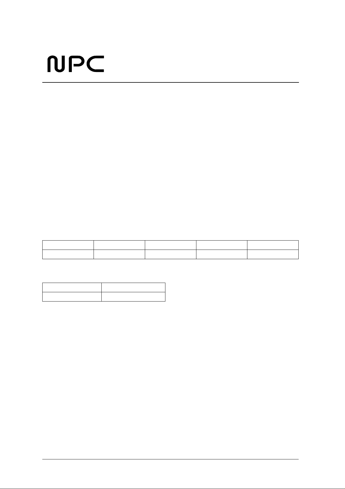
PAD LAYOUT
(Unit : µ m)
CF5008A1
UNUSED2
UNUSED1
XT2
VDD
INH
(1400,1300)
1234 5
(0,0)
78
XTVSS
Chip size: 1.40
Chip thickness: 220 ± 30 µm
Chip base: V
DD
level
6
Q
1.30 mm
PAD DIMENSIONS
Number Name I/O Description
1 UNUSED1 – Not used. 153 1112
2 UNUSED2 – Not used. 425 1112
3XT2 O Oscillator output pin 66 0 1112
4 VD D – Supply voltage 865 1112
5 INH
6 Q O Output pin 1245 152
7 X T I Oscillator input pin 34 6 18 8
8 VSS – Ground 155 188
Output-control input pin. Q signal output enabled when HIGH
I
or open. High-impedance output when LOW.
Pad dimensions [µm]
XY
1202 1112
NIPPON PRECISION CIRCUITS—2
Page 3
Ω
Ω
Ω
Ω
Ω
BLOCK DIAGRAM
CF5008A1
Rf
XT
XT2
CG
RB2
CD Rd
CC
Control Circuits
VDD
VSS
Q
Rp
INH
OSCILLATOR ELEMENT CONSTANTS (typical values)
R
B1
CF5008A1 100k
R
50k
B2
R
450
d
R
f
150k
R
100k
p
C
G
20pF 10pF 70pF
C
D
C
C
NIPPON PRECISION CIRCUITS—3
Page 4

−
−
SPECIFICATIONS
Absolute Maximum Ratings
V
= 0 V
SS
Parameter Symbol Condition Rating Unit
Supply voltage range V
Input voltage range V
Output voltage range V
Operating temperature range T
Storage temperature range T
Output current I
−
OUT
−
DD
IN
OUT
opr
stg
°
−
°
−
°
CF5008A1
0.5 to 7.0 V
0.5 to V
0.5 to V
+ 0.5 V
DD
+ 0.5 V
DD
40 to 85
65 to 150
25 mA
C
C
Recommended Operating Conditions
V
= 0 V, CL ≤ 15 pF, f ≤ 32.5 MHz
SS
Parameter Symbol Condition
Supply voltage V
Input voltage V
Operating temperature T
DD
IN
OPR
Rating
min typ ma x
2.7 – 5.5 V
V
SS
–V
DD
20 – 80
Unit
V
C
NIPPON PRECISION CIRCUITS—4
Page 5

Electrical Characteristics
≤
V
= 4.5 to 5.5 V, V
DD
= 0 V, Ta = − 20 to 80 ° C unless otherwise noted.
SS
CF5008A1
Ω
Ω
Ω
Ω
Ω
Ω
°
Parameter Symbol Condition
HIGH-level output voltage V
L O W-level output voltage V
Q: Measurement cct 1, I
OH
Q: Measurement cct 1, I
OL
Q: Measurement cct 2, IN H = LO W, V
Output leakage current I
HIGH-level input voltage V
L O W -level input voltage V
Current consumption I
INH pull-up resistance R
Feedback resistance R
Built-in resistance
Built-in capacitance
Z
Q: Measurement cct 2, IN H = LO W, V
INH 0.8V
IH
INH – – 0.2V
IL
INH = open, Measurement cct 3, load cct 1, C
DD
Measurement cct 4 50 – 150 k
UP
Design value, determined by the internal wafer pattern – 1 5 0 – k
f
R
d
Design value, determined by the internal wafer pattern
R
c
R
Measurement cct 5 – 10 0 – k
B1
R
Measurement cct 6 – 50 – k
B2
C
G
Design value, determined by the internal wafer pattern
C
D
C
C
= 8 mA, V
OH
= 8 mA, V
OL
Rating
min typ max
= 4.5 V 4.0 4.2 – V
DD
= 4.5 V – 0.3 0.4 V
DD
= V
OH
DD
= V
OL
SS
= 15 pF, f = 30 MHz – 28 65 mA
L
––10
––10
––V
DD
DD
– 450 –
–0–
–20–pF
–10–pF
–70–pF
Unit
µA
V
Switching Characteristics
V
= 2.7 to 5.5 V, V
DD
= 0 V, Ta = − 20 to 80 ° C unless otherwise noted.
SS
Rating
Parameter Symbol Condition
min typ max
V
= 2.7 to 3.6 V – 3 8
C,
DD
V
= 4.5 to 5.5 V – 2.5 6
DD
V
= 2.7 to 3.6 V – 3 8
DD
V
= 4.5 to 5.5 V – 2.5 6
DD
= 3.0 V 42 – 58
V
DD
V
= 5.0 V 42 – 58
DD
– – 100 ns
15 pF
L
– – 100 ns
Output rise time t
Output fall time t
Output duty cycle
1
Output disable delay time t
Output enable delay time t
Measurement cct 3, load cct 1,
r1
0.1V
to 0.9V
DD
Measurement cct 3, load cct 1,
f1
0.9V
to 0.1V
DD
Measurement cct 3, load cct 1, Ta = 25
Duty
C
= 15 pF, f = 32MHz
L
PLZ
Measurement cct 7, load cct 1, Ta = 25 ° C, C
PZL
DD
DD
, C
, C
= 15 p F
L
= 15 p F
L
1. Determined by the lot monitor.
Current consumption and Output waveform with NPC’s standard crystal
Cb
f (MHz) R (Ω) L (mH) Ca (fF) Cb (pF)
30 17.2 4.36 6.46 2.26
Unit
ns
ns
%
L
Ca R
NIPPON PRECISION CIRCUITS—5
Page 6

CF5008A1
FUNCTIONAL DESCRIPTION
Standby Function
The oscillator output on Q changes as shown in the following table when INH goes LOW.
INH Q Oscillator
HIGH (or open) f
O
LO W High impedance Normal operation
Nor mal operation
TYPICAL APPLICATION CIRCUIT
Typical circuit structures (C
and C
G
) that use a varicap device have a reduced frequency range due to the
D
effects of parasitic capacitance. The CF5008A1, however, has built-in components C
nected in series with the varicap device, increasing the frequency output range.
VCXO Module
Rf
CG
RB2
CD Rd
CC
Rp
Control Circuits
CF5008
Control
Input
XT
X'tal
VARI−CAP
XT2
PARASITIC CAPACITANCE
and R
C
VDD
VSS
Q
INH
that are con-
B2
VCC
GND
Output
Output
Enable
Parasitic capacitance are unwanted capacitance effects that occur due to the junction capacitance where the
protection diodes and transistor drains are connected to the substrate. The following equivalent circuit figure
shows the calculated parasitic capacitances. The surface area for each component is calculated from the IC layout pattern, and the capacitance calculated per unit area.
Rf 150k
CG
XT2
5.01p
4.7p
RB2
50k
20p
XT
C
10p
C
70p
2.4p
Divider
(1/1)
Rd
D
C
Rp
Control
Circuits
100k
VDD
VSS
Q
INHN
NIPPON PRECISION CIRCUITS—6
Page 7

CF5008A1
VARICAP (Variable Capacitance Diodes) SELECTION
The CF5008A1 forms a VCXO with addition of an external varicap (variable capacitance diode) device. This
section examines the results using various varicap devices. When the equivalent circuit in figure 1 is used, the
load capacitance C
Varicap devices that can change the capacitance by a factor of 5 require a maximum capacitance in the range
approximately 20 to 50pF. Devices matching this criteria are listed in the following table.
must be changed by a factor of 4 to 5 (10 to 40pF) to affect a ±100ppm frequency change.
L
=
=
=
=
=
L
4.08673mH
Frequency:28.633MHz
Ca
7.56439fF
Cb
2.05389pF
C
:20pF
L
R
17.7068Ω
Figure 1. Crystal oscillator element equivalent circuit
Company Product Capacitance 1 Capacitance 2
HITACHI HVU17 50.0 to 85.0pF (VR
HITACHI HVU359 24.8 to 29.8pF (VR
HITACHI HVU362 41.6 to 49.9pF (VR
HITACHI HVC374B 21.5 to 24.0pF (VR = 1V) 12.5 to 14.5pF (VR = 2V)
HITACHI HVC375B 15.5 to 17.0pF (VR = 1V) 4.0pF typ (VR = 4V)
Panasonic MA304 24.8 to 29.8pF (VR = 1V) 6.00 to 8.30pF (VR = 4V)
Panasonic MA2S304 24.8 to 29.8pF (VR = 1V) 6.00 to 8.30pF (VR = 4V)
Panasonic MA2ZV05 18.5 to 20.5pF (VR = 1V) 3.60 to 4.10pF (VR = 4V)
TOKO KV1811E 21.5pF typ (VR
TOKO KV1812 16.0pF typ (VR = 1V) 3.00pF typ (VR = 4V)
1V) 5.23 to 8.84pF (VR
1V) 6.00 to 8.30pF (VR
1V) 10.1 to 14.8pF (VR
=
1V) 4.00pF typ (VR = 4V)
4.5V)
4V)
4V)
=
NIPPON PRECISION CIRCUITS—7
Page 8

MEASUREMENT CIRCUITS
CF5008A1
Measurement cct 1
Signal
Generator
XT input waveform
(10MHz)
Q output
Q output
C1 : 0.001µF
R1 : 50
R2 : 500
R3 : 512.5
C1
R1
Ω
Ω
Ω
Measurement cct 2
VDD
XT Q
VSS
When
measuring VOL
When
measuring VOH
VDD
0V
VDD
VOH
0V
VDD
VOL
0V
Measurement cct 4
R3
R2
A
Measurement cct 5
A
IRUP
IRB1
INH
XT1
VCNOT
VDD
VSS
VDD
VSS
RUP =
RB1 =
VDD
IRUP
VDD
IRB1
VDD
INH
VSS
Measurement cct 3
XT
X'tal
C3
XT2
Q
INH
A
VDD
IZ
V
VSS
IZ
IDD
Measurement cct 6
A
XT2
VDD
VSS
RB2 =
VDD
IRB2
A
IRB2
Measurement cct 7
Q
Signal
Generator
C1
R1
VDD
XT Q
VSS
INH
C3 : 15pF
C1 : 0.001µF
R1 : 50
Ω
NIPPON PRECISION CIRCUITS—8
Page 9

Load cct 1
CF5008A1
Q output
CL
(Including probe capacity)
CL = 15pF : I
Switching Time Measurement Waveform
Output duty level (CMOS)
0.9VDD
Q output
0.1VDD
tr tf
Output duty cycle (CMOS)
Q output
TW
T
TW
DD
, DUTY, t
r1
, t
f1
0.9VDD
0.1VDD
DUTY measuring
voltage (0.5V
DUTY measuring
voltage
DUTY= T
W/ T 100 (%)
DD)
(0.5VDD)
Output Enable/Disable Delay
INH
Q output
VIL
tPLZ
INH inputwaveform tr = tf 10ns
VIH
tPZL
NIPPON PRECISION CIRCUITS—9
Page 10

CF5008A1
NIPPON PRECISION CIRCUITS INC. reserves the right to make changes to the products described in this data sheet in order to
improve the design or performance and to supply the best possible products. Nippon Precision Circuits Inc. assumes no responsibility for
the use of any circuits shown in this data sheet, conveys no license under any patent or other rights, and makes no claim that the circuits
are free from patent infringement. Applications for any devices shown in this data sheet are for illustration only and Nippon Precision
Circuits Inc. makes no claim or warranty that such applications will be suitable for the use specified without further testing or modification.
The products described in this data sheet are not intended to use for the apparatus which influence human lives due to the failure or
malfunction of the products. Customers are requested to comply with applicable laws and regulations in effect now and hereinafter,
including compliance with export controls on the distribution or dissemination of the products. Customers shall not export, directly or
indirectly, any products without first obtaining required licenses and approvals from appropriate government agencies.
NIPPON PRECISION CIRCUITS INC.
4-3, Fukuzumi 2-chome
Koto-ku, Tokyo 135-8430, Japan
NIPPON PRECISION CIRCUITS INC.
Telephone: 03-3642-6661
Facsimile: 03-3642-6698
NC9816AE 1999.09
NIPPON PRECISION CIRCUITS—10
 Loading...