

Page 1
© 1999 Fairchild Semiconductor Corporation DS005987 www.fairchildsemi.com
October 1987
Revised July 1999
CD40174BC • CD40175BC Hex D-Type Flip-Flop • Quad D-Type Flip-Flop
CD40174BC • CD40175BC
Hex D-Type Flip-Flop • Quad D-Type Flip-Flop
General Description
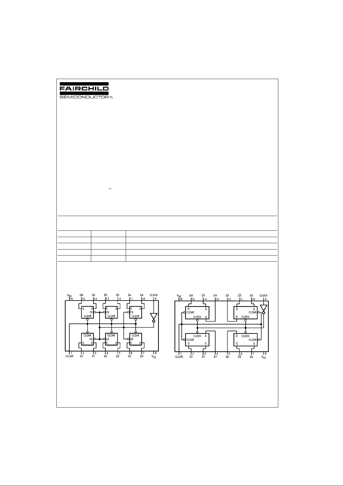
The CD40174BC con sis ts o f six po si tive- ed ge tri g ger ed Dtype fli p-flops; the true outputs from each fli p-flop are externally available. The CD40175BC consists of four positiveedge triggered D-typ e flip-flo ps; both the tr ue and co mplement outputs from each flip-flop are externally available.
All flip-flops are controlled by a common clock a nd a common clear. Information at the D inputs meeti ng the set-up
time requirements is transferred to the Q outputs on the
positive-going edge of the clock pulse. The clea ring op er ation, enabled by a ne gative pulse at Clear inpu t, clears all
Q outputs to logical “0” and Q
s (CD40175BC only) to logi-
cal “1”.
All inputs are protected from static discharge by diode
clamps to V
DD
and VSS.
Features
■ Wide supply voltage range: 3V to 15V
■ High noise immunity: 0.45 V
DD
(typ.)
■ Low power TTL compatibility:
fan out of 2 driving 74L or 1 driving 74 LS
■ Equivalent to MC14174B, MC14175B
■ Equivalent to MM74C174, MM74C175
Ordering Code:
Devices also availab le in Tape and Reel. Specify by appending th e s uffix let t er “X” to the ordering code.
Connection Diagrams
Pin Assignments for DIP and SOIC
CD40174B
Top View
CD40175B
Top View
Order Number Package Number Package Description
CD40174BCM M16A 16-Lead Small Outline Integrated Circuit (SOIC), JEDEC MS-012, 0.150” Narrow Body
CD40174BCN N16E 16-Lead Plastic Dual-In-Line Package (PDIP), JEDEC MS-001, 0.300” Wide
CD40175BCM M16A 16-Lead Small Outline Integrated Circuit (SOIC), JEDEC MS-012, 0.150” Narrow Body
CD40175BCN N16E 16-Lead Plastic Dual-In-Line Package (PDIP), JEDEC MS-001, 0.300” Wide
Page 2
www.fairchildsemi.com 2
CD40174BC • CD40175BC
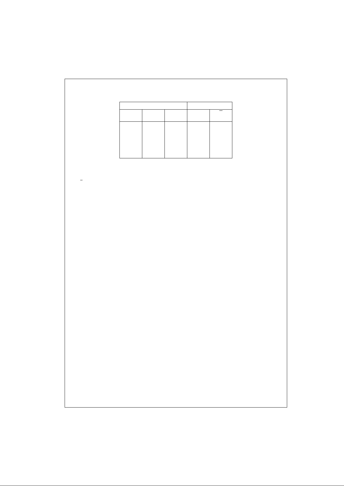
Truth Table
H = HIGH Level
L = LOW Level
X = Irrelevant
↑ = Transition from LOW-to-HIGH lev el
NC = No change
Note 1: Q
for CD40175B only
Inputs Outputs
Clear Clock D Q Q
(Note 1)
LXXLH
H ↑ HHL
H ↑ LLH
HHXNCNC
HLXNCNC
Page 3
3 www.fairchildsemi.com
CD40174BC • CD40175BC
Absolute Maximum Ratings(Note 2)
(Note 3)
Recommended Operating
Conditions
(Note 3)
Note 2: “Absolute Maximum Ratings” are those values beyond which the
safety of the device can not be guaranteed. T hey are not meant to imply
that the devices should be operated at these lim its. The tab les of “Recom mended Operating Conditions” and “Electrical Characteristics” provide conditions for actual dev ic e operation.
Note 3: V
SS
= 0V unless otherw is e s pecified.
DC Electrical Characteristics (Note 3)
CD40174BC/CD40175BC
Note 4: IOH and IOL are tested one output at a ti m e.
DC Supply Voltage (VDD) −0.5V to +18V
Input Voltage (V
IN
) −0.5V to VDD +0.5V
DC
Storage Temperature Range (TS) −65°C to +150°C
Power Dissipation (P
D
)
Dual-In-Line 700 mW
Small Outline 500 mW
Lead Temperatu re (T
L
)
(Soldering, 10 seconds) 260°C
DC Supply Voltage (V
DD
) 3V to 15 V
DC
Input Voltage (VIN) 0V to VDD V
DC
Operating Temperature Range (TA) −40°C to +85°C
Symbol Parameter Conditions
−40°C +25°C +85°C
Units
Min Max Min Typ Max Min Max
I
DD
Quiescent Device VDD = 5V, VIN = VDD or V
SS
4430µA
Current VDD = 10V, VIN = VDD or V
SS
8860µA
VDD = 15V, VIN = VDD or V
SS
16 16 120 µA
V
OL
LOW Level VDD = 5V 0.05 0.05 0.05 V
Output Voltage VDD = 10V 0.05 0.05 0.05 V
VDD = 15V 0.05 0.05 0.05 V
V
OH
HIGH Level VDD = 5V 4.95 4.95 5 4.95 V
Output Voltage VDD = 10V 9.95 9.95 10 9.95 V
VDD = 15V 14.95 14.95 15 14.95 V
V
IL
LOW Level VDD = 5V, VO = 0.5V or 4.5V 1.5 1.5 1.5 V
Input Voltage VDD = 10V, VO = 1V or 9V 3.0 3.0 3.0 V
VDD = 15V, VO = 1.5V or 13.5V 4.0 4.0 4.0 V
V
IH
HIGH Level VDD = 5V, VO = 0.5V or 4.5V 3.5 3.5 3.5 V
Input Voltage VDD = 10V, VO = 1V or 9V 7.0 7.0 7.0 V
VDD = 15V, VO = 1.5V or 13.5V 11.0 11.0 11.0 V
I
OL
LOW Level Output VDD = 5V, VO = 0.4V 0.52 0.44 0.88 0. 36 mA
Current (Note 4) VDD = 10V, VO = 0.5V 1.3 1.1 2.25 0.9 mA
VDD = 15V, VO = 1.5V 3.6 3.0 8.8 2.4 mA
I
OH
HIGH Level Output VDD = 5V, VO = 4.6V −0.52 −0.44 −0.88 −0.36 mA
Current (Note 4) VDD = 10V, VO = 9.5V −1.3 −1.1 −2.25 −0.9 mA
VDD = 15V, VO = 13.5V −3.6 −3.0 −8.8 −2.4 mA
I
IN
Input Current VDD = 15V, VIN = 0V −0.30 −10−5−0.30 −1.0 µA
VDD = 15V, VIN = 15V 0.30 10−50.30 1.0 µA
Page 4

www.fairchildsemi.com 4
CD40174BC • CD40175BC
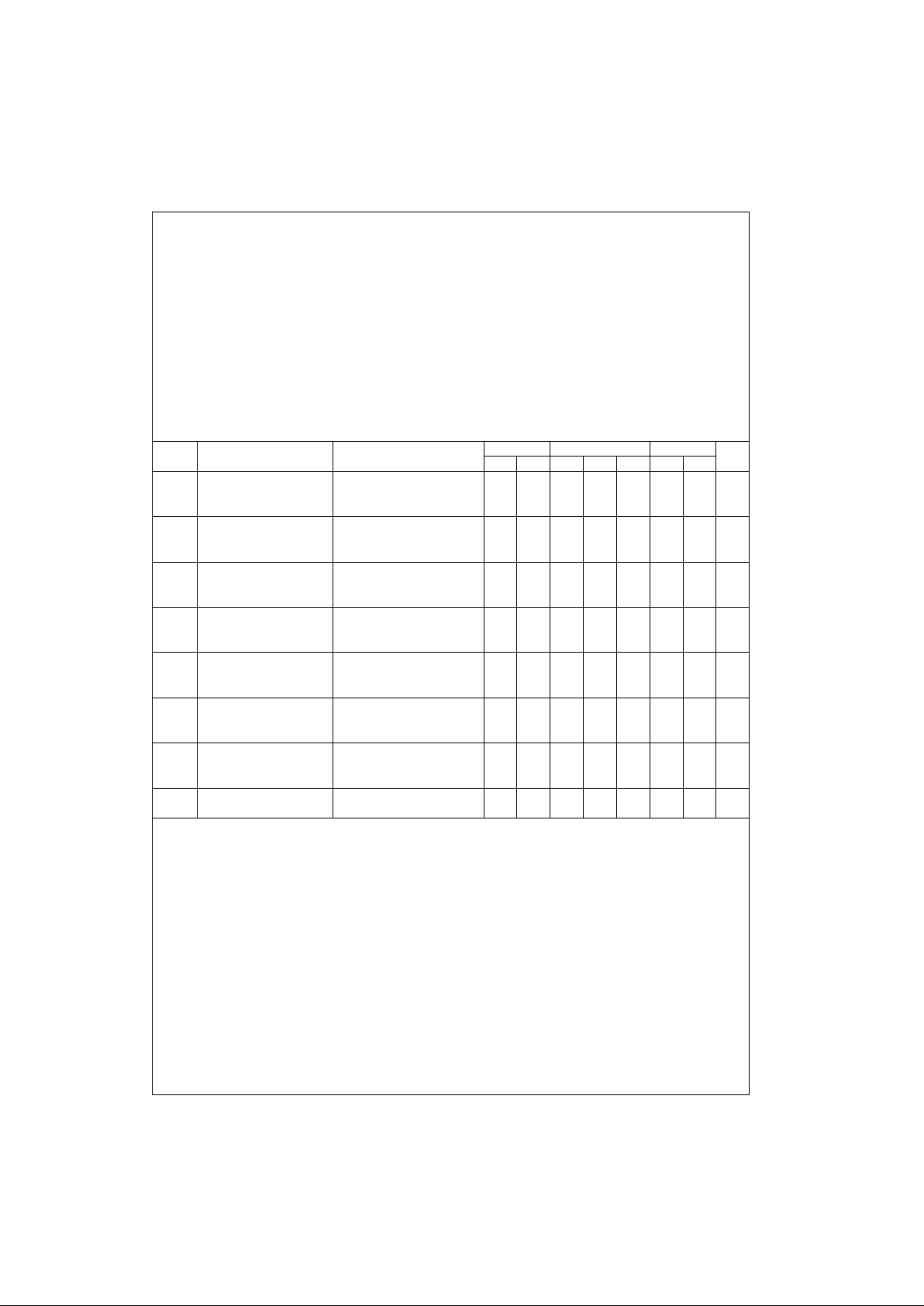
AC Electrical Characteristics (Note 5)
TA = 25°C, CL = 50 pF, RL = 200k and tr = tf = 20 ns, unless otherwise specified
Note 5: AC Parame t ers are guaranteed by DC c orrelated testing.
Note 6: C
PD
determines the no load AC power con sumption o f any CM OS device. For com plete explan ation, see 74C Fam ily Characte ristics ap plication
note, AN-90.
Symbol Parameter Conditions Min Typ Max Units
t
PHL
, t
PLH
Propagation Delay Time to a VDD = 5V 190 300 ns
Logical “0” or Logical “1” from VDD = 10V 75 110 ns
Clock to Q or Q (CD40175 Only) VDD = 15V 60 90 ns
t
PHL
Propagation Delay Time to a VDD = 5V 180 300 ns
Logical “0” from Clear to Q VDD = 10V 70 110 ns
VDD = 15V 60 90 ns
t
PLH
Propagation Delay Time to a Logical VDD = 5V 230 400 ns
“1” from Clear to Q (CD40175 Only) VDD = 10V 90 150 ns
VDD = 15V 75 120 ns
t
SU
Time Prior to Clock Pulse that VDD = 5V 45 100 ns
Data must be Present VDD = 10V 15 40 ns
VDD = 15V 13 35 ns
t
H
Time after Clock Pulse that VDD = 5V −11 0 ns
Data Must be Held VDD = 10V −40 ns
VDD = 15V −30 ns
t
THL
, t
TLH
Transition Time VDD = 5V 100 200 ns
VDD = 10V 50 100 ns
VDD = 15V 40 80 ns
tWH, t
WL
Minimum Clock Pulse Width VDD = 5V 130 250 ns
VDD = 10V 45 100 ns
VDD = 15V 40 80 ns
t
WL
Minimum Clear Pulse Width VDD = 5V 120 250 ns
VDD = 10V 45 100 ns
VDD = 15V 40 80 ns
t
RCL
Maximum Clock Rise Time VDD = 5V 15 µs
VDD = 10V 5.0 µs
VDD = 15V 5.0 µs
t
fCL
Maximum Clock Fall Time VDD = 5V 15 50 µs
VDD = 10V 5.0 50 µs
VDD = 15V 5.0 50 µs
f
CL
Maximum Clock Frequency VDD = 5V 2.0 3.5 MHz
VDD = 10V 5.0 10 MHz
VDD = 15V 6.0 12 MHz
C
IN
Input Capacitance Clear Input 10 15 pF
Other Input 5.0 7.5 pF
C
PD
Power Dissipation Per Package (Note 6) 130 pF
Page 5

5 www.fairchildsemi.com
CD40174BC • CD40175BC
Switching Time Wavef orms
tr = tf = 20 ns
Page 6

www.fairchildsemi.com 6
CD40174BC • CD40175BC
Physical Dimensions inches (millimeters) unless otherwise noted
16-Lead Small Outline Integrated Circuit (SOIC), JEDEC MS-012, 0.150” Narrow Body
Package Number M16A
Page 7

7 www.fairchildsemi.com
CD40174BC • CD40175BC Hex D-Type Flip-Flop • Quad D-T ype Flip-Flop
Physical Dimensions inches (millimeters) unless otherwise noted (Continued)
16-Lead Plastic Dual-In-Line Package (PDIP), JEDEC MS-001, 0.300” Wide
Package Number N16E
Fairchild does not assume any responsibility for use of any circu itry described, no circuit patent license s are implied and
Fairchild reserves the right at any time without notice to change said circuitry and specifications.
LIFE SUPPORT POLICY
FAIRCHILD’S PRODUCTS ARE NOT AUTHORIZED FOR USE AS CRITICAL COMPONENTS IN LIFE SUPPORT
DEVICES OR SYSTEMS WITHOUT THE EXPRESS WRITTEN APPROVAL OF THE PRESIDENT OF FAIRCHILD
SEMICONDUCTOR CORPORATION. As used herein:
1. Life support devices or systems are dev ic es or syste ms
which, (a) are intended for surgical implant into the
body, or (b) support or sustain life, and (c) whose failure
to perform when properly used in accordance with
instructions for use provided i n the labe li ng, can be re asonably expected to result in a significant injury to the
user.
2. A critical componen t in any com ponent o f a l ife supp ort
device or system whose failu re to perform can b e reasonably expected to c ause th e fa i lure of the li fe s upp or t
device or system, or to affect its safety or effectiveness.
www.fairchildsemi.com
 Loading...