

Page 1
November 1983
Revised January 1999
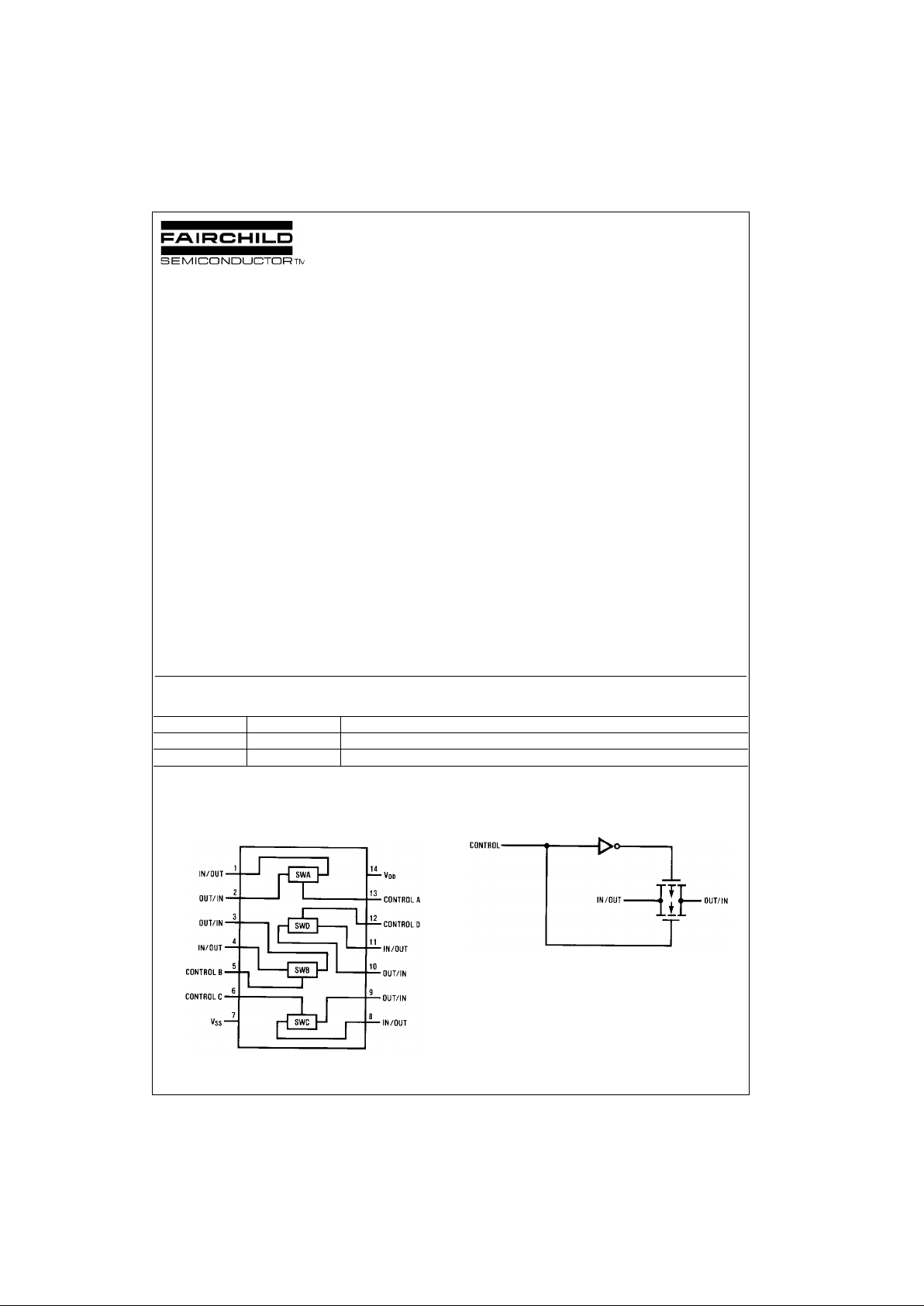
CD4016BC Quad Bilateral Switch
© 1999 Fairchild Semiconductor Corporation DS005661.prf www.fairchildsemi.com
CD4016BC
Quad Bilateral Switch
General Description
The CD4016BC is a quad bilate ral switch intended for the
transmission or multiplexing of analog or digital signals. It is
pin-for-pin compatible with CD4066BC.
Features
■ Wide supply voltage range: 3V to 15V
■ Wide range of digital and analog switching: ±7.5 V
PEAK
■ “ON” resistance for 15V operation: 400Ω (typ.)
■ Matched “ON” resistance over 15V signal input:
∆R
ON
= 10Ω (typ.)
■ High degree of linearity:
0.4% distortion (typ.)
@ f
IS
= 1 kHz, V
IS
= 5 V
p-p
,
V
DD−VSS
= 10V, RL = 10 kΩ
■ Extremely low “OFF” switch leakage:
0.1 nA (typ.)
@ V
DD
− V
SS
= 10V
T
A
= 25°C
■ Extremely high control input impedance: 10
12
Ω (typ.)
■ Low crosstalk between switches:
−50 dB (typ.)
@ f
IS
= 0.9 MHz, RL = 1 kΩ
■ Frequency response, switch “ON”: 40 MHz (typ.)
Applications
• Analog signal switching/multiplexing
Signal gating
Squelch control
Chopper
Modulator/Demodulator
Commutating switch
• Digital signal switching/multiplexing
• CMOS logic implementation
• Analog-to-digital/digital-to-analog conversion
• Digital control of frequency, impedance, phase, and ana-
log-signal gain
Ordering Code:
Devices also available in Tape and Reel. Specify by appending the letter suffix “X” to t he ordering code.
Connection Diagram
Pin Assignments for DIP and SOIC
Schematic Diagram
Order Number Package Number Package Description
CD4016BCM M14A 14-Lead Small Outline Integrated Circuit (SOIC), JEDEC MS-120, 0.150” Narrow
CD4016BCN N14A 14-Lead Plastic Dual-In-Line Package (PDIP), JEDEC MS-001, 0.300” Wide
Page 2
www.fairchildsemi.com 2
CD4016BC
Absolute Maximum Ratings(Note 1)
(Note 2)
Recommended Operating
Conditions
(Note 2)
Note 1: “Absolute Maxi mum Ratings” are those valu es beyond which the
safety of the device cannot be guaranteed. They are not meant to imply
that the devices should be o perated at these lim its. The table s of “Recom mended Operating Conditions” and “Electrical Cha rac t eristics” provide conditions for actual device operation.
Note 2: V
SS
= 0V unless otherwis e specified.
DC Electrical Characteristics (Note 2)
Note 3: If the switch input is held at VDD, V
IHC
is the contro l input level that will cause the switch out put to meet the standard “B” s eries VOH and IOH output
levels. If the analog switch input is connected to V
SS
, V
IHC
is the control input level — which allows the switch to sink standard “B” series |IOH|, high level cur-
rent, and still maint ain a V
OL
≤ “B” series. These c urrents are shown in Figur e 8.
VDD Supply Voltage −0.5V to +18V
V
IN
Input Voltage −0.5V to VDD + 0.5V
T
S
Storage Temperature Range −65°C to + 150°C
Power Dissipation (P
D
)
Dual-In-Line 700 mW
Small Outline 500 mW
Lead Temperature
(Soldering, 10 seconds) 260°C
V
DD
Supply Voltage 3V to 15V
V
IN
Input Voltage 0V to V
DD
TA Operating Temperature Range −40°C to +85°C
Symbol Parameter Conditions
−40°C25°C +85°C
Units
Min Max Min Typ Max Min Max
I
DD
Quiescent Device V
DD
= 5V, VIN = VDD or V
SS
1.0 0.01 1.0 7.5 µA
Current V
DD
= 10V, V
IN
= VDD or V
SS
2.0 0.01 2.0 15 µA
V
DD
= 15V, VIN = VDD or V
SS
4.0 0.01 4.0 30 µA
Signal Inputs and Outputs
R
ON
“ON” Resistance RL = 10kΩ to (VDD − VSS)/2
VC = VDD, V
IS
= VSS or V
DD
V
DD
= 10V 610 275 660 840 Ω
V
DD
= 15V 370 200 400 520 Ω
RL = 10kΩ to (VDD − VSS)/2
VC = V
DD
V
DD
= 10V, V
IS
= 4.75 to 5.25V 1900 850 2000 2380 Ω
V
DD
= 15V, V
IS
= 7.25 to 7.75V 790 400 850 1080 Ω
∆R
ON
∆“ON” Resistance RL = 10kΩ to (VDD − VSS)/2
Between any 2 of VC = VDD, V
IS
= VSS to V
DD
4 Switches V
DD
= 10V 15 Ω
(In Same Package) V
DD
= 15V 10 Ω
I
IS
Input or Output VC = 0, VDD = 15V ±50 ±0.1 ±50 ±200 nA
Leakage V
IS
= 0V or 15V,
Switch “OFF” V
OS
= 15V or 0V
Control Inputs
V
ILC
LOW Level Input V
IS
= VSS and V
DD
Voltage V
OS
= VDD and V
SS
I
IS
= ±10 µA
V
DD
= 5V 0.9 0.7 0.4 V
V
DD
= 10V 0.9 0.7 0.4 V
V
DD
= 15V 0.9 0.7 0.4 V
V
IHC
HIGH Level Input V
DD
= 5V 3.5 3.5 3.5 V
Voltage V
DD
= 10V 7.0 7.0 7.0 V
V
DD
= 15V 11.0 11.0 11.0 V
(Note 3) and Figure 8
I
IN
Input Current V
CC
− V
SS
= 15V ±0.3 ±10−5±0.3 ±1.0 µA
V
DD
≥ V
IS
≥ V
SS
V
DD
≥ VC ≥ V
SS
Page 3
3 www.fairchildsemi.com
CD4016BC
AC Electrical Characteristics (Note 4)
T
A
= 25°C, tr = tf = 20 ns and V
SS
= 0V unless otherwise specified
Note 4: AC Parameters are guaranteed by DC correlated testing.
Note 5: These devices should not be connected to circuits with the power “ON”.
Note 6: In all cases, th ere is approximately 5 p F of probe and jig capacit ance on the output; how ever, this capacitance is included in C
L
wherever it is specified.
Note 7: V
IS
is the voltage at the in/out pin and VOS is the voltage at the out/in pi n. VC is the voltage at the contro l input.
Symbol Parameter Conditions Min Typ Max Units
t
PHL
, t
PLH
Propagation Delay Time VC = VDD, CL = 50 pF, (Figure 1)
Signal Input to Signal Output RL = 200k
V
DD
= 5V 58 100 ns
VDD= 10V 27 50 ns
V
DD
= 15V 20 40 ns
t
PZH
, t
PZL
Propagation Delay Time RL = 1.0 kΩ, CL = 50 pF, (Figure 2, Figure 3)
Control Input to Signal V
DD
= 5V 20 50 ns
Output HIGH Impedance to VDD = 10V 18 40 ns
Logical Level V
DD
= 15V 17 35 ns
t
PHZ
, t
PLZ
Propagation Delay Time RL = 1.0 kΩ, CL = 50 pF, (Figure 2, Figure 3)
Control Input to Signal V
DD
= 5V 15 40 ns
Output Logical Level to V
DD
= 10V 11 25 ns
HIGH Impedance V
DD
= 15V 10 22 ns
Sine Wave Distortion VC = V
DD
= 5V, VSS = −50.4%
RL = 10 kΩ, V
IS
= 5 V
P-P
, f = 1 kHz,
(Figure 4)
Frequency Response — Switch VC = V
DD
= 5V, V
SS
= −5V, 40 MHz
“ON” (Frequency at −3 dB) RL = 1 kΩ, V
IS
= 5 V
P-P
,
20 Log10 VOS/VOS (1 kHz) −dB,
(Figure 4)
Feedthrough — Switch “OFF” V
DD
= 5V, VC = V
SS
= −5V, 1.25 MHz
(Frequency at −50 dB) RL = 1 kΩ, V
IS
= 5 V
P-P
,
20 Log10 (VOS/VIS) = −50 dB,
(Figure 4)
Crosstalk Between Any T wo V
DD
= V
C(A)
= 5V; V
SS
= V
C(B)
= −5V, 0.9 MHz
Switches (Frequency at −50 dB) RL = 1 kΩV
IS(A)
= 5 V
P-P
,
20 Log10 (V
OS(B)/VOS(A)
) = −50 dB,
(Figure 5)
Crosstalk; Control Input to V
DD
= 10V, RL = 10 kΩ 150 mV
P-P
Signal Output R
IN
= 1 kΩ, VCC = 10V Square Wave,
CL = 50 pF (Figure 6)
Maximum Control Input RL = 1 kΩ, CL = 50 pF, (Figure 7)
V
OS(f)
= ½ VOS(1 kHz)
V
DD
= 5V 6.5 MHz
V
DD
= 10V 8.0 MHz
V
DD
= 15V 9.0 MHz
C
IS
Signal Input Capacitance 4pF
C
OS
Signal Output Capacitance V
DD
= 10V 4 pF
C
IOS
Feedthrough Capacitance VC = 0V 0.2 pF
C
IN
Control Input Capacitance 57.5 pF
Page 4

www.fairchildsemi.com 4
CD4016BC
AC Test Circuits and Switching Time Wavef orms
FIGURE 1. t
PLH
, t
PLH
Propagation Delay Time Control to Signal Output
FIGURE 2. t
PZH
, t
PHZ
Propagation Delay Time Control to Signal Output
FIGURE 3. t
PZH
, t
PHZ
Propagation Delay Time Control to Signal Output
VC = VDD for distortion and frequency response te s ts
V
C
= VSS for feedthrough test
FIGURE 4. Sine Wave Distortion, Frequency Response and Feedthrough
Page 5

5 www.fairchildsemi.com
CD4016BC
AC Test Circuits and Switching Time Waveforms (Continued)
FIGURE 5. Crosstalk Between Any Two Switches
FIGURE 6. Crosstalk — Control to Input Signal Output
FIGURE 7. Maximum Contro l Input Frequency
Page 6

www.fairchildsemi.com 6
CD4016BC
AC Test Circuits and Switching Time Wavef orms (Continued)
FIGURE 8. CD4016B Switch Test Conditions for V
IHC
Typical Performance Characteristics
’ON’ Resistance vs. Signal
Voltage T
A
= 25°C
’ON’ Resistance Temperature
Variation for V
DD
− V
SS
= 10V
’ON’ Resistance Temperature
Variation for V
DD
− V
SS
= 15V
Temperature Switch Input Switch Output
Range
V
DD
V
IS
IIS (mA) VOS(V)
−40°C25°C +85°CMin Max
5 0 0.2 0.16 0.12 0.4
55−0.2 −0.16 −0.12 4.6
COMMERCIAL 10 0 0.5 0.4 0.3 0.5
10 10 −0.5 −0.4 −0.3 9.5
15 0 1.4 1.2 1.0 1.5
15 15 −1.4 −1.2 −1.0 13.5
Page 7

7 www.fairchildsemi.com
CD4016BC
Typical Applications
4 Input Multiplexer
Sample/Hold Amplifier
Special Considerations
The CD4016B is composed of 4, two-transistor analog
switches. These switches do not have any linea rization or
compensation circuitry for “R
ON
” as do the CD4066B's.
Because of this, the special ope rating considerations for
the CD4066B do not apply to the CD4016B, but at low supply voltages, ≤5V, the CD4016B's on resistance becom es
non-linear. It is recommended that at 5V , v oltages on the in/
out pins be mainta ined within about 1V of either V
DD
or
V
SS
; and that at 3V the voltages on the in /out pins should
be at V
DD
or VSS for reliable operation.
Page 8

www.fairchildsemi.com 8
CD4016BC
Physical Dimensions inches (millimeters) unless otherwise noted
14-Lead Small Outline Integrated Circuit (SOIC), JEDEC MS-120, 0.150” Narrow
Package Number M14A
Page 9

Fairchild does not assume any responsibility for use of any circuitry described, no circuit patent licenses are implied and Fairchild reser ves the right at any time without notice to change said circuitry and specifications.
CD4016BC Quad Bilateral Switch
LIFE SUPPORT POLICY
FAIRCHILD’S PRODUCTS ARE NOT AUTHORIZED FOR USE AS CRITICAL COMPONENTS IN LIFE SUPPORT
DEVICES OR SYSTEMS WITHOUT THE EXPRESS WRITTEN APPROVAL OF THE PRESIDENT OF FAIRCHILD
SEMICONDUCTOR CORPORATION. As used herein:
1. Life support devices or system s a re devices or syste ms
which, (a) are intended for surgical implant into the
body, or (b) support or sustain life, and (c) whose failure
to perform when properly used in accordance with
instructions for use provided in the labeling, can be reasonably expected to result in a significant injur y to the
user.
2. A critical compon ent in any com ponent of a li fe support
device or system whose failure to p erform can be r easonably expected to cause the failure of the life suppor t
device or system, or to affect its safety or effectiveness.
www.fairchildsemi.com
Physical Dimensions inches (millimeters) unless otherwise noted (Continued)
14-Lead Plastic Dual-In-Line Package (PDIP), JEDEC MS-001, 0.300” Wide
Package Number N14A
 Loading...