

Page 1
CD4015BT
Data Sheet July 1999 File Number
CMOS Dual 4-Stage Static Shift Register
With Serial Input/Parallel Output
Intersil’sSatellite Applications FlowTM(SAF) devices are fully
tested and guaranteed to 100kRAD total dose. These QML
Class T devices are processed to a standard flow intended
to meet the cost and shorter lead-time needs of large
volume satellite manufacturers, while maintaining a high
level of reliability.
CD4015BT consists of two identical, independent, 4-stage
serial-input/parallel output registers. Each register has
independent CLOCK and RESET inputs as well as a single
serial DATA input. “Q” outputs are available from each of the
four stages on both registers. All register stages are D type,
master-slave flip-flops. The logic level present at the DATA
input is transferred into the first register stage and shifted
over one stage at each positive-going clock transition.
Resetting of all stages is accomplished by a high level on the
reset line. Register expansion to 8 stages using one
CD4015BT, or to more than 8 stages using additional
CD4015BT’s is possible.
Specifications
Specifications for Rad Hard QML devices are controlled by
the Defense Supply Center in Columbus (DSCC). The SMD
numbers listed below must be used when ordering.
Detailed Electrical Specifications for the CD4015BT are
contained in SMD 5962-96624. A “hot-link” is provided from
our website for downloading.
www.intersil.com/spacedefense/ne wsafc lasst.asp
4621.1
Features
• QML Class T, Per MIL-PRF-38535
• Radiation Performance
5
- Gamma Dose (γ) 1 x 10
- SEP Effective LET > 75 MEV/gm/cm
• Medium Speed Operation 12MHz (typ.)Clock Rate at V
RAD(Si)
2
DD
- VSS = 10V
• Fully Static Operation
• 8 Master-Slave Flip-Flops Plus Input and Output Buffering
• 100% Tested For Quiescent Current at 20V
• 5V, 10V and 15V Parametric Ratings
• Standardized Symmetrical Output Characteristics
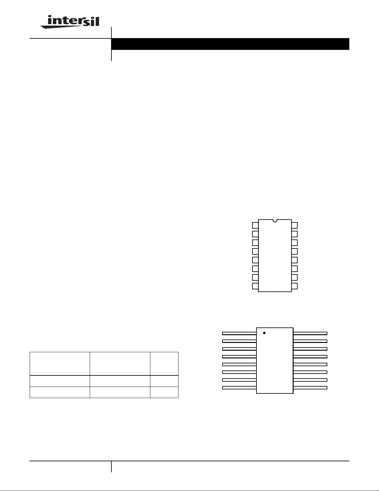
Pinouts
CD4015BT (SBDIP), CDIP2-T16
TOP VIEW
V
CLOCK B
Q4B
Q3A
Q2A
Q1A
RESET A
DATA A
V
SS
1
2
3
4
5
6
7
8
16
15
DATA B
14
RESET B
13
Q1B
12
Q2B
Q3B
11
10
Q4A
9
CLOCK A
DD
Intersil’s Quality Management Plan (QM Plan), listing all
Class T screening operations, is also available on our
website.
www.intersil.com/quality/manuals.asp
Ordering Information
TEMP.
ORDERING
NUMBER
5962R9662401TEC CD4015BDTR -55 to 125
5962R9662401TXC CD4015BKTR -55 to 125
NOTE:
Minimumorderquantity for -T is 150 units through
distribution, or 450 units direct.
PART
NUMBER
1
RANGE
(oC)
CAUTION: These devices are sensitive to electrostatic discharge; follow proper IC Handling Procedures.
CD4015BT (FLATPACK), CDFP4-F16
TOP VIEW
CLOCK B
Q4B
Q3A
Q2A
Q1A
RESET A
DATA A
V
SS
www.intersil.com or 407-727-9207
Satellite Applications Flow™ (SAF) is a trademark of Intersil Corporation.
116
2
3
4
5
6
7
8
15
14
13
12
11
10
9
| Copyright © Intersil Corporation 1999
V
DD
DATA B
RESET B
Q1B
Q2B
Q3B
Q4A
CLOCK A
Page 2
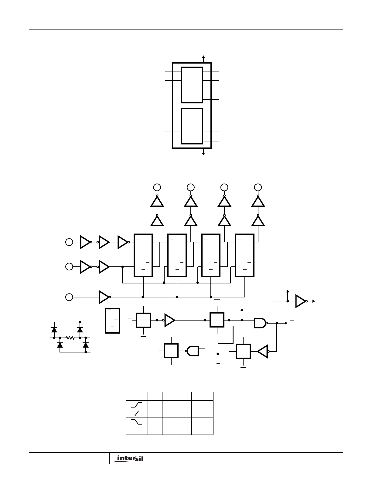
Functional Diagram
Logic Diagram
CD4015BT
V
DD
16
DATA A
CLOCK A
RESET A
DATA B
CLOCK B
RESET B
7
9
6
15
1
14
13Q1 (5) 12Q2 (4) 11Q3 (3) 2Q4 (10)
4
STAGE
4
STAGE
5
Q1A
4
Q2A
3
Q3A
10
Q4A
13
Q1B
12
Q2B
11
Q3B
2
Q4B
8
V
SS
DAT A
15
†
(7)
CLOCK
1
†
(9)
RESET
14
†
(6)
DQ
V
†ALL INPUTS ARE PROTECTED
BY CMOS PROTECTION
NETWORK
DD
CL
V
SS
D
≡
Q
R
CL D R Q1 Qn
X = Don’t care Case
DQ
QCL
R
CL
p
n
CL
DQ
QCL
R
CL
p
n
CL
DQ
QCL
R
TRUTH TABLE
0 0 0 Qn-1
1 0 1 Qn-1
X 0 Q1 Qn (No Change)
XX100
CL
CL
DQ
QCL
R
CL
Q
p
n
CL
p
n
R
CL
CL
Q
CL
2
Page 3

Die Characteristics
CD4015BT
DIE DIMENSIONS:
(2032µm x 2489µm x 533µm ±25.4µm)
80 x 98 x 21mils ±1mil
METALLIZATION:
Type: Al
Thickness: 12.5k
Å ±1.5kÅ
SUBSTRATE POTENTIAL:
Leave Floating or Tie to V
Bond Pad #16 (VDD) First
DD;
BACKSIDE FINISH:
Silicon
Metallization Mask Layout
PASSIVATION:
Type: Phosphorus Doped Silox (S
Thickness: 13k
Å ±2.6kÅ
iO2
)
WORST CASE CURRENT DENSITY:
< 2.0e5 A/cm
2
TRANSISTOR COUNT:
60
PROCESS:
Bulk CMOS
CD4015BT
80mils
1
3
2
4
16
15
14
5
98mils
13
6
7
8 9
12
1110
All Intersil semiconductor products are manufactured, assembled and tested under ISO9000 quality systems certification.
Intersil semiconductor products are sold by description only. Intersil Corporation reserves the right to make changes in circuit design and/or specifications at any time without notice. Accordingly, the reader is cautioned to verify that data sheets are current before placing orders. Information furnished by Intersil is believed to be accurate and
reliable. However ,no responsibility is assumed by Intersil or its subsidiaries for its use; nor for any infringements of patents or other rights of third parties which may result
from its use. No license is granted by implication or otherwise under any patent or patent rights of Intersil or its subsidiaries.
For information regarding Intersil Corporation and its products, see web site http://www.intersil.com
3
 Loading...