

Page 1
October 1987
Revised January 1999
CD4015BC Dual 4-Bit Static Shift Register
© 1999 Fairchild Semiconductor Corporation DS005948.prf www.fairchildsemi.com
CD4015BC
Dual 4-Bit Static Shift Register
General Description
The CD4015BC contains two identical, 4-stage, serial-
input/parallel-output registers with independent “Data”,
“Clock,” and “Reset” inputs. Th e logic level present at the
input of each stage is transferred to the output of that stage
at each positive-going clock transition. A logi c high on the
“Reset” input resets al l four stages covered by that input.
All inputs are protected from static discharge by a series
resistor and diode clamps to V
DD
and VSS.
Features
■ Wide supply voltage range: 3.0V to 18V
■ High noise immunity: 0.45 V
DD
(typ.)
■ Low power TTL: Fan out of 2 driving 74L
compatibility: or 1 driving 74LS
■ Medium speed operation: 8 MHz (typ.) clock rate
■ Fully static design: @V
DD
− VSS = 10V
Applications
• Serial-input/parallel-output data queueing
• Serial to parallel data conversion
• General purpose register
Ordering Code:
Devices also available in Tape and Reel. Specify by appending the suffix letter “X” to the ordering code.
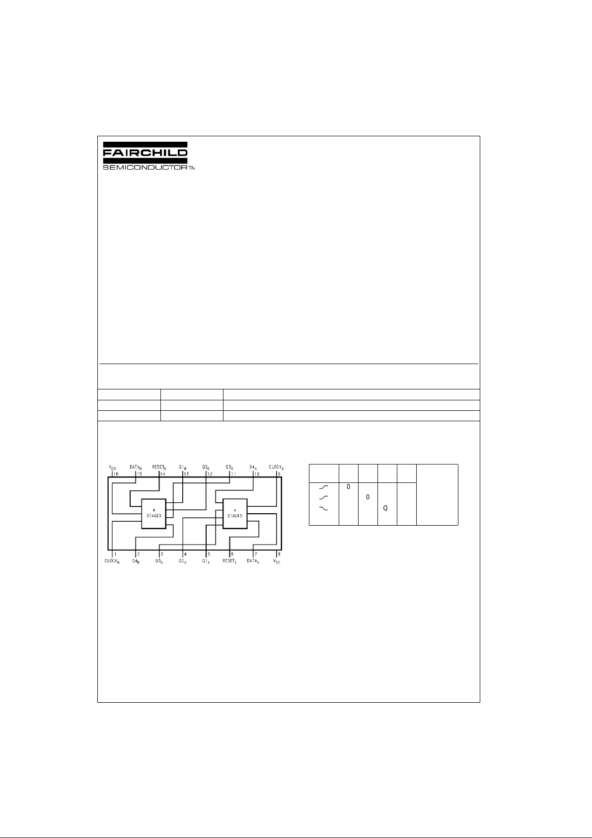
Connection Diagram
Pin Assignments for DIP and SOIC
Truth Table
X = Don't Care Case
Note 1: Level Change
Order Number Package Number Package Description
CD4015BCM M16A 16-Lead Small Outline Integrated Circuit (SOIC), JEDEC MS-012, 0.150” Narrow
CD4015BCN N16E 16-Lead Plastic Dual-In-Line Package (PDIP), JEDEC MS-001, 0.300” Wide
CL
(Note 1)
DRQ1Q
n
000Q
n−1
101Q
n−1
X0Q1Qn(No change)
XX100
Page 2
www.fairchildsemi.com 2
CD4015BC
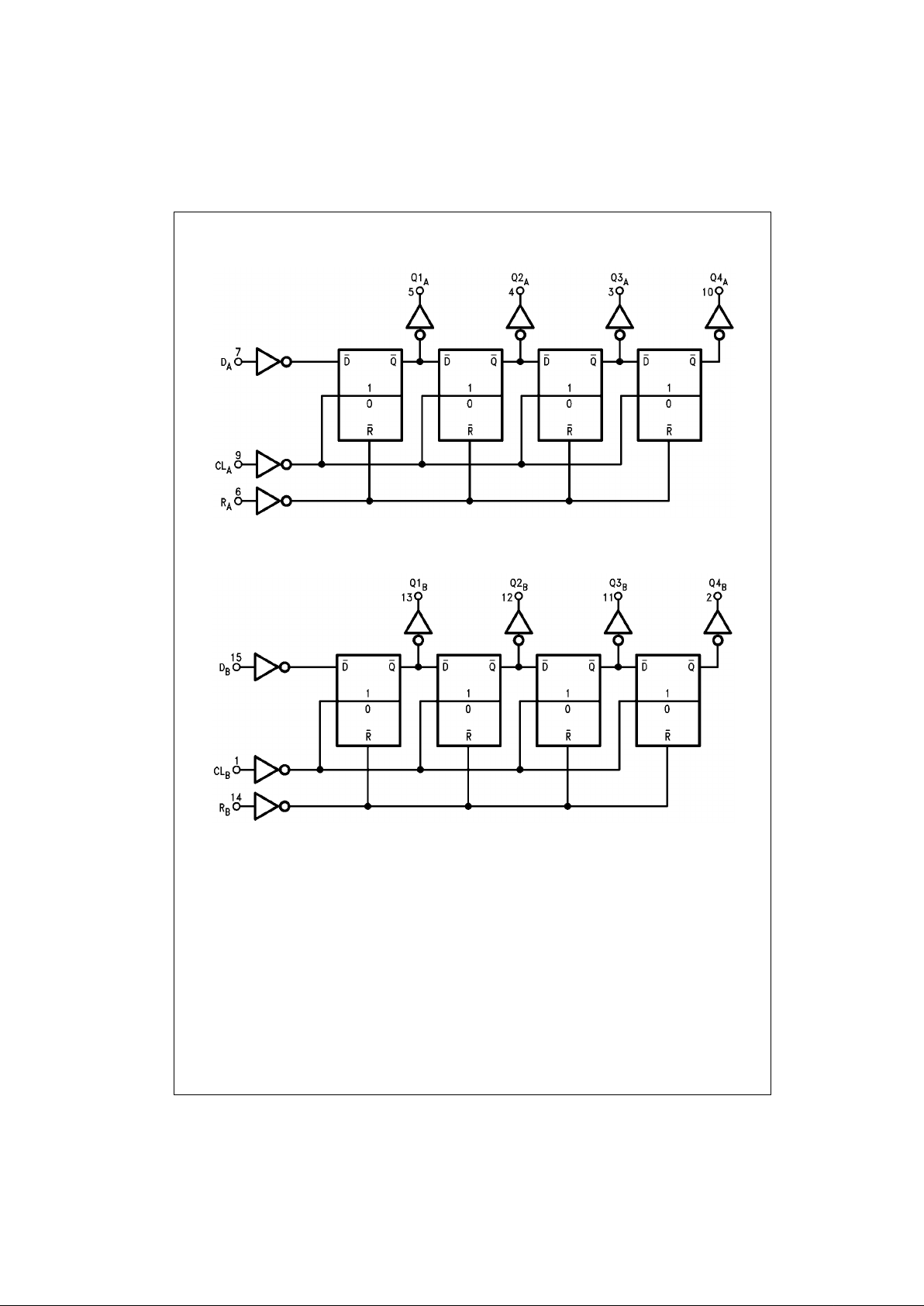
Logic Diagrams
Terminal No. 16 = V
DD
Terminal No. 8 = GND
Page 3

3 www.fairchildsemi.com
CD4015BC
Absolute Maximum Ratings(Note 2)
(Note 3)
Recommended Operating
Conditions
Note 2: “Absolute Maximum Rat ings” are tho se values beyond which the
safety of the device cannot be guaranteed; they are not meant to imply that
the devices should be o perated at these limits. The tables of “R ecommended Operating Conditions” and “Electrical Characteristics” provide conditions for actual device operat ion.
Note 3: V
SS
= 0V unless otherw is e s pecified.
DC Electrical Characteristics (Note 3)
Note 4: IOH and IOL are tested one output at a ti m e.
DC Supply Voltage (VDD) −0.5 to +18 V
DC
Input Voltage (VIN) −0.5 to VDD +0.5 V
DC
Storage Temperature Range (TS) −65°C to +150°C
Power Dissipation (P
D
)
Dual-In-Line 700 mW
Small Outline 500 mW
Lead Temperature (T
L
)
(Soldering , 10 seconds) 260°C
DC Supply Voltage (V
DD
) +3 to +15 V
DC
Input Voltage (VIN) 0 to VDD V
DC
Operating Temperature Range (TA) −40°C to +85°C
Symbol Parameter Conditions
−40°C +25°C +85°C
Units
Min Max Min Typ Max Min Max
I
DD
Quiescent Device VDD = 5V, VIN = VDD or V
SS
20 0.005 20 150 µA
Current VDD = 10V, VIN = VDD or V
SS
40 0.010 40 300 µA
VDD = 15V, VIN = VDD or V
SS
80 0.015 80 600 µA
V
OL
LOW Level VDD = 5V 0.05 0 0.05 0.05 V
Output Voltage VDD = 10V 0.05 0 0.05 0.05 V
VDD = 15V 0.05 0 0.05 0.05 V
V
OH
HIGH Level VDD = 5V 4.95 4.95 5 4.95 V
Output Voltage VDD = 10V 9.95 9.95 10 9.95 V
VDD = 15V 14.95 14.95 15 14.95 V
V
IL
LOW Level VDD = 5V, VO = 0.5V or 4.5V 1.5 2.25 1.5 1.5 V
Input Voltage VDD = 10V, VO = 1.0V or 9.0V 3.0 4.50 3 .0 3.0 V
VDD = 15V, VO = 1.5V or 13.5V 4.0 6.75 4.0 4.0 V
V
IH
HIGH Level VDD = 5V, VO = 0.5V or 4.5V 3.5 3.5 2.75 3.5 V
Input Voltage VDD = 10V, VO = 1.0V or 9.0V 7.0 7.0 5.50 7.0 V
VDD = 15V, VO = 1.5V or 13.5V 11.0 11.0 8.25 11.0 V
I
OL
LOW Level Output VDD = 5V, VO = 0.4V 0.52 0.44 0.88 0.36 mA
Current (Note 4) VDD = 10V, VO = 0.5V 1.3 1.1 2.25 0.9 mA
VDD = 15V, VO = 1.5V 3.6 3.0 8.8 2.4 mA
I
OH
HIGH Level Output VDD = 5V, VO = 4.6V −0.52 −0.44 −0.88 −0.36 mA
Current (Note 4) VDD = 10V, VO = 9.5V −1.3 −1.1 −2.25 −0.9 mA
VDD = 15V, VO = 13.5V −3.6 −3.0 −8.8 −2.4 mA
I
IN
Input Current VDD = 15V, VIN = 0V −0.3 −10−5−0.3 −1.0 µA
VDD = 15V, VIN = 15V 0.3 10−50.3 1.0 µA
Page 4

www.fairchildsemi.com 4
CD4015BC
AC Electrical Charac teristics (Note 5)
T
A
= 25°C, CL= 50 pF, RL= 200k, t
r
= tf = 20 ns, unless otherwise specified
Note 5: AC Parameters are guara nt eed by DC correlated testin g.
Symbol Parameter Conditions Min Typ Max Units
CLOCK OPERATION
t
PHL
, t
PLH
Propagation Delay Time VDD = 5V 230 350 ns
VDD = 10V 80 160 ns
VDD = 15V 60 120 ns
t
THL
, t
TLH
Transition Time VDD = 5V 100 200 ns
VDD = 10V 50 100 ns
VDD = 15V 40 80 ns
tWL, t
WM
Minimum Clock VDD = 5V 160 250 ns
Pulse-Width VDD = 10V 60 110 ns
VDD = 15V 50 85 ns
t
rCL
, t
fCL
Clock Rise and VDD = 5V 15 µs
Fall Time VDD = 10V 15 µs
VDD = 15V 15 µs
t
SU
Minimum Data VDD = 5V 50 100 µs
Set-Up Time VDD = 10V 20 40 µs
VDD = 15V 15 30 µs
f
CL
Maximum Clock VDD = 5V 2 3.5 MHz
Frequency VDD = 10V 4.5 8 MHz
VDD = 15V 6 11 MHz
C
IN
Input Capacitance Clock Input 7.5 10 pF
Other Inputs 5 7.5 pF
RESET OPERATION
t
PHL(R)
Propagation Delay Time VDD = 5V 200 400 ns
VDD = 10V 100 200 ns
VDD = 15V 80 160 ns
t
WH(R)
Minimum Reset VDD = 5V 135 250 ns
Pulse Width VDD = 10V 40 80 ns
VDD = 15V 30 60 ns
Page 5

5 www.fairchildsemi.com
CD4015BC
Physical Dimensions inches (millimeters) unless otherwise noted
16-Lead Small Outline Integrated Circuit (SOIC), JEDEC MS-012, 0.150” Narrow
Package Number M16A
Page 6

Fairchild does not assume any responsibility for use of any circuitry descri bed, no circuit patent licenses are implied and Fairchil d reser ves the right at any time without notice to change said circuitr y and specifications.
CD4015BC Dual 4-Bit Static Shift Register
LIFE SUPPORT POLICY
FAIRCHILD’S PRODUCTS ARE NOT AUTHORIZED FOR USE AS CRITICAL COMPONENTS IN LIFE SUPPORT
DEVICES OR SYSTEMS WITHOUT THE EXPRESS WRITTEN APPROVAL OF THE PRESIDENT OF FAIRCHILD
SEMICONDUCTOR CORPORATION. As used herein:
1. Life support devices or system s ar e devices or syste ms
which, (a) are intended for surgical implant into the
body, or (b) support or sustain life, and (c) whose failure
to perform when properly used in accordance with
instructions for use provided in the labeling, can be reasonably expected to result in a significant injury to the
user.
2. A critical component in any c omponent of a life suppor t
device or system whose failure to perform can be reasonably expected to cause the failure of the life suppor t
device or system, or to affect its safety or effectiveness.
www.fairchildsemi.com
Physical Dimensions inches (millimeters) unless otherwise noted (Continued)
16-Lead Plastic Dual-In-Line Package (PDIP), JEDEC MS-001, 0.300” Wide
Package Number N16E
 Loading...