

Page 1
Product
Folder
Sample &
Buy
Technical
Documents
Tools &
Software
Support &
Community
CC1020
SWRS046H –NOVEMBER 2006–REVISED MARCH 2015
CC1020 Low-Power RF Transceiver for Narrowband Systems
1 Device Overview
1.1 Features
1
• True Single Chip UHF RF Transceiver • Pb-Free Package
• Frequency Range 402 MHz to 470 MHz • Digital RSSI and Carrier Sense Indicator
and 804 MHz to 960 MHz
• High Sensitivity
– Up to –118 dBm for a 12.5 kHz Channel
• Programmable Output Power
• Low Current Consumption
– RX: 19.9 mA Temperature Drift Compensation Possible Without
• Low Supply Voltage
– 2.3 V to 3.6 V
• No External IF Filter Needed
• Low-IF Receiver
• Very Few External Components Required
• Small Size
– QFN 32 Package
• Data Rate up to 153.6 kBaud
• OOK, FSK, and GFSK Data Modulation
• Integrated Bit Synchronizer
• Image Rejection Mixer
• Programmable Frequency and AFC Make Crystal
TCXO
• Suitable for Frequency Hopping Systems
• Suited for Systems Targeting Compliance With
EN 300 220, FCC CFR47 Part 15, ARIB STD-T67,
and ARIB STD-T96
• Development Kit Available
• Easy-to-Use Software for Generating the CC1020
Configuration Data
1.2 Applications
• Narrowband Low-Power UHF Wireless Data • AMR – Automatic Meter Reading
Transmitters and Receivers With Channel
Spacing as Low as 12.5 and 25 kHz
• 402-, 424-, 426-, 429-, 433-, 447-, 449-, 469-,
868-, 915-, 960-MHz ISM/SRD Band Systems
• Wireless Alarm and Security Systems
• Home Automation
• Low Power Telemetry
1.3 Description
CC1020 is a true single-chip UHF transceiver designed for very low-power and very low-voltage wireless
applications. The circuit is mainly intended for the ISM (Industrial, Scientific, and Medical) and SRD (Short
Range Device) frequency bands at 402-, 424-, 426-, 429-, 433-, 447-, 449-, 469-, 868-, 915-, and 960MHz, but can easily be programmed for multichannel operation at other frequencies in the 402- to 470MHz and 804- to 960-MHz range.
The CC1020 device is especially suited for narrow-band systems with channel spacing of 12.5 or 25 kHz
complying with ARIB STD-T67 and EN 300 220.
The main operating parameters of the CC1020 device can be programmed with a serial bus, thus making
CC1020 a very flexible and easy-to-use transceiver.
In a typical system, the CC1020 device will be used together with a microcontroller and a few external
passive components.
TI recommends using the latest RF performance line device CC1120 as successor of CC1020:
www.ti.com/rfperformanceline
Table 1-1. Device Information
PART NUMBER PACKAGE BODY SIZE (NOM)
CC1020 VQFNP (32) 7.00 mm × 7.00 mm
1
(1) For more information, see Section 8, Mechanical Packaging and Orderable Information.
An IMPORTANT NOTICE at the end of this data sheet addresses availability, warranty, changes, use in safety-critical applications,
intellectual property matters and other important disclaimers. PRODUCTION DATA.
(1)
Page 2
RF_IN
LNA
FREQ
SYNTH
DIGITAL
DEMODULATOR
- Digital RSSI
- Gain Control
- Image Suppression
- Channel Filtering
- Demodulation
DIGITAL
MODULATOR
- Modulation
- Data shaping
- Power Control
BIAS
Power
Control
DIGITAL
INTERFACE
TO mC
CONTROL
LOGIC
PA
ADC
ADC
RF_OUT
R_BIAS
XOSC_Q1 XOSC_Q2
PDO
XOSC
VC
CHP_OUT
LNA 2
0
90
:2
0
90
:2
Multiplexer
Multiplexer
PA_EN
LNA_EN
PCLK
PDI
PSEL
CC1020
SWRS046H –NOVEMBER 2006–REVISED MARCH 2015
1.4 Functional Block Diagram
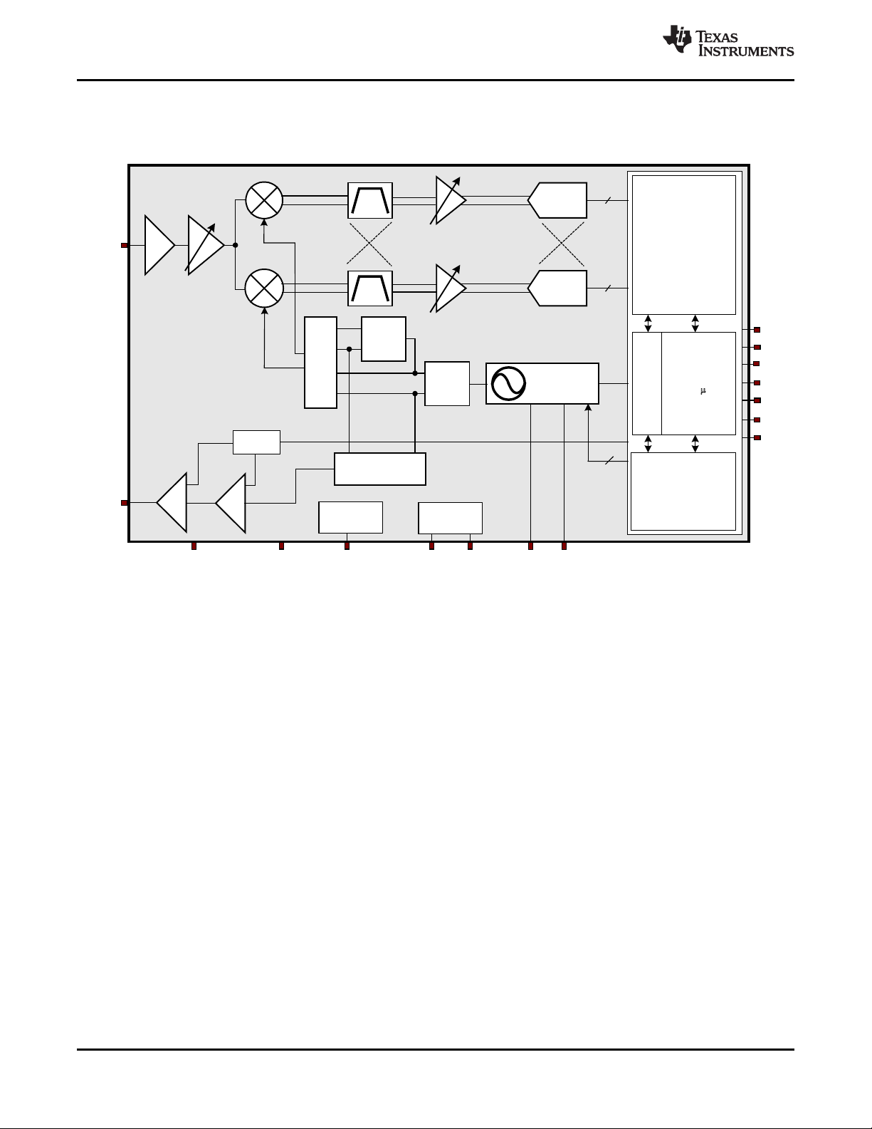
Figure 1-1 shows the system block diagram of the CC1020 device.
www.ti.com
Figure 1-1. Functional Block Diagram
2 Device Overview Copyright © 2006–2015, Texas Instruments Incorporated
Submit Documentation Feedback
Product Folder Links: CC1020
Page 3

CC1020
www.ti.com
SWRS046H –NOVEMBER 2006–REVISED MARCH 2015
Table of Contents
1 Device Overview ......................................... 1 5.7 Data Rate Programming ............................ 24
1.1 Features .............................................. 1 5.8 Frequency Programming ............................ 26
1.2 Applications........................................... 1 5.9 Receiver............................................. 27
1.3 Description............................................ 1 5.10 Transmitter .......................................... 39
1.4 Functional Block Diagram ............................ 2 5.11 Input and Output Matching and Filtering............ 42
2 Revision History ......................................... 4 5.12 Frequency Synthesizer.............................. 45
3 Terminal Configuration and Functions.............. 5 5.13 VCO and LNA Current Control...................... 51
3.1 Pin Diagram .......................................... 5 5.14 Power Management................................. 51
3.2 Pin Configuration ..................................... 5 5.15 On-Off Keying (OOK) ............................... 53
4 Specifications ............................................ 7 5.16 Crystal Oscillator .................................... 55
4.1 Absolute Maximum Ratings .......................... 7 5.17 Built-in Test Pattern Generator ..................... 56
4.2 ESD Ratings.......................................... 7 5.18 Interrupt on Pin DCLK............................... 56
4.3 Recommended Operating Conditions................ 7 5.19 PA_EN and LNA_EN Digital Output Pins........... 57
4.4 RF Transmit .......................................... 8 5.20 System Considerations and Guidelines............. 58
4.5 RF Receive ........................................... 9 5.21 Antenna Considerations............................. 61
4.6 RSSI / Carrier Sense................................ 12 5.22 Configuration Registers ............................. 62
4.7 Intermediate Frequency (IF) ........................ 12 6 Applications, Implementation, and Layout........ 83
4.8 Crystal Oscillator .................................... 13 6.1 Application Information.............................. 83
4.9 Frequency Synthesizer.............................. 14 6.2 Design Requirements ............................... 85
4.10 Digital Inputs and Outputs .......................... 15 6.3 PCB Layout Recommendations..................... 86
4.11 Current Consumption ............................... 16 7 Device and Documentation Support ............... 87
4.12 Thermal Resistance Characteristics for VQFNP
Package ............................................. 16
5 Detailed Description ................................... 17
5.1 Overview ............................................ 17
5.2 Functional Block Diagram........................... 17
5.3 Configuration Overview ............................. 18
5.4 Microcontroller Interface............................. 19
5.5 4-wire Serial Configuration Interface................ 20
5.6 Signal Interface...................................... 21
7.1 Device Support...................................... 87
7.2 Documentation Support ............................. 87
7.3 Trademarks.......................................... 88
7.4 Electrostatic Discharge Caution..................... 88
7.5 Export Control Notice ............................... 88
7.6 Glossary............................................. 88
8 Mechanical Packaging and Orderable
Information .............................................. 88
8.1 Packaging Information .............................. 88
Copyright © 2006–2015, Texas Instruments Incorporated Table of Contents 3
Submit Documentation Feedback
Product Folder Links: CC1020
Page 4
CC1020
SWRS046H –NOVEMBER 2006–REVISED MARCH 2015
www.ti.com
2 Revision History
This data manual revision history highlights the changes made to the SWRS046F device-specific data
manual to make it an SWRS046G revision.
Changes from Revision F (January 2006) to Revision G Page
• Converted document to new TI standards......................................................................................... 1
• Added Thermal Resistance Characteristics for VQFNP Package. ........................................................... 16
• Changed Register table format to new TI standards. .......................................................................... 62
Changes from January 19, 2015 to February 19, 2015 Page
• Updated RUZ package to RSS.................................................................................................... 87
4 Revision History Copyright © 2006–2015, Texas Instruments Incorporated
Submit Documentation Feedback
Product Folder Links: CC1020
Page 5
PCLK 1
VC
24
AVDD
23
AVDD
22
RF_OUT
21
AVDD
20
RF_IN
19
AVDD
18
R_BIAS
17
AVDD
16
PA_EN
15
LNA_EN
14
AVDD
13
AVDD
12
XOSC_Q2
11
XOSC_Q1
10
LOCK
9
DIO
8
DCLK
7
DGND
6
DVDD
5
DGND
4
PDO
3
PDI
2
32
PSEL
31
DVDD
30
DGND
29
AVDD
28
CHP_OUT
27
AVDD
26
AD_REF
25
AGND
AGND
Exposed die
attached pad
www.ti.com
3 Terminal Configuration and Functions
3.1 Pin Diagram
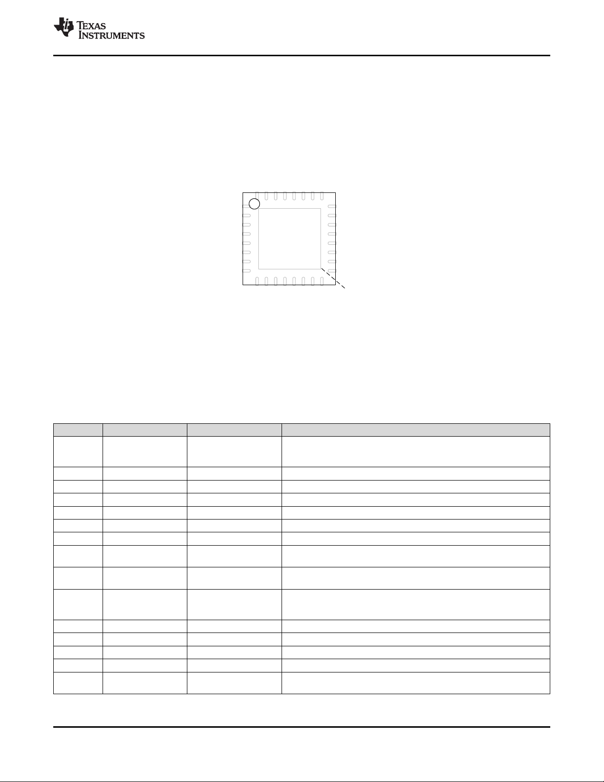
Figure 3-1 shows pin names and locations for the CC1020 device.
The CC1020 comes in a QFN 32-type package.
CC1020
SWRS046H –NOVEMBER 2006–REVISED MARCH 2015
Figure 3-1. Package 7-mm × 7-mm VQFNP (Top View)
3.2 Pin Configuration
Table 3-1 provides an overview of the CC1020 pinout.
Table 3-1. Pin Attributes
PIN NO. PIN NAME TYPE DESCRIPTION
— AGND Ground (analog) this is the ground connection for all analog modules. See Section 6.3 for
1 PCLK Digital input Programming clock for SPI configuration interface
2 PDI Digital input Programming data input for SPI configuration interface
3 PDO Digital output Programming data output for SPI configuration interface
4 DGND Ground (digital) Ground connection (0 V) for digital modules and digital I/O
5 DVDD Power (digital) Power supply (3 V typical) for digital modules and digital I/O
6 DGND Ground (digital) Ground connection (0 V) for digital modules (substrate)
7 DCLK Digital output
8 DIO Digital input/output
9 LOCK Digital output lock. The pin can also be used as a general digital output, or as receive
10 XOSC_Q1 Analog input Crystal oscillator or external clock input
11 XOSC_Q2 Analog output Crystal oscillator
12 AVDD Power (analog) Power supply (3 V typical) for crystal oscillator
13 AVDD Power (analog) Power supply (3 V typical) for the IF VGA
14 LNA_EN Digital output
(1) DCLK, DIO and LOCK are high-impedance (3-state) in power down (BIAS_PD = 1 in the MAIN register).
(2) The exposed die attached pad must be soldered to a solid ground plane as this is the main ground connection for the chip.
Copyright © 2006–2015, Texas Instruments Incorporated Terminal Configuration and Functions 5
Submit Documentation Feedback
Product Folder Links: CC1020
Exposed die attached pad. Must be soldered to a solid ground plane as
more details.
Clock for data in both receive and transmit mode.
Can be used as receive data output in asynchronous mode
Data input in transmit mode; data output in receive mode.
Can also be used to start power-up sequencing in receive
PLL Lock indicator, active low. Output is asserted (low) when PLL is in
data output in synchronous NRZ/Manchester mode
General digital output. Can be used for controlling an external LNA if
higher sensitivity is needed.
(1)(2)
Page 6
CC1020
SWRS046H –NOVEMBER 2006–REVISED MARCH 2015
www.ti.com
Table 3-1. Pin Attributes
PIN NO. PIN NAME TYPE DESCRIPTION
15 PA_EN Digital output
16 AVDD Power (analog) Power supply (3 V typical) for global bias generator and IF anti-alias filter
17 R_BIAS Analog output Connection for external precision bias resistor (82 kΩ, ±1%)
18 AVDD Power (analog) Power supply (3 V typical) for LNA input stage
19 RF_IN RF Input RF signal input from antenna (external AC-coupling)
20 AVDD Power (analog) Power supply (3 V typical) for LNA
21 RF_OUT RF output RF signal output to antenna
22 AVDD Power (analog)
23 AVDD Power (analog) Power supply (3 V typical) for VCO
24 VC Analog input VCO control voltage input from external loop filter
25 AGND Ground (analog) Ground connection (0 V) for analog modules (guard)
26 AD_REF Power (analog) 3 V reference input for ADC
27 AVDD Power (analog) Power supply (3 V typical) for charge pump and phase detector
28 CHP_OUT Analog output PLL charge pump output to external loop filter
29 AVDD Power (analog) Power supply (3 V typical) for ADC
30 DGND Ground (digital) Ground connection (0 V) for digital modules (guard)
31 DVDD Power (digital) Power supply connection (3 V typical) for digital modules
32 PSEL Digital input
General digital output. Can be used for controlling an external PA if higher
output power is needed.
Power supply (3 V typical) for LO buffers, mixers, prescaler, and first PA
stage
Programming chip select, active low, for configuration interface. Internal
pullup resistor.
(1)(2)
(continued)
6 Terminal Configuration and Functions Copyright © 2006–2015, Texas Instruments Incorporated
Submit Documentation Feedback
Product Folder Links: CC1020
Page 7

www.ti.com
4 Specifications
CC1020
SWRS046H –NOVEMBER 2006–REVISED MARCH 2015
4.1 Absolute Maximum Ratings
PARAMETER MIN MAX UNIT CONDITION
Supply voltage, VDD –0.3 5.0 V
Voltage on any pin –0.3 V
Input RF level 10 dBm
Package body temperature 260 °C Norm: IPC/JEDEC J-STD-020
Humidity non-condensing 5% 85%
Storage temperature range, T
(1) Stresses beyond those listed under absolute maximum ratings may cause permanent damage to the device. These are stress ratings
only, and functional operation of the device at these or any other conditions beyond those indicated under general characteristics is not
implied. Exposure to absolute-maximum-rated conditions for extended periods may affect device reliability.
(2) The reflow peak soldering temperature (body temperature) is specified according to IPC/JEDEC J-STD_020 “Moisture/Reflow Sensitivity
Classification for Nonhermetic Solid State Surface Mount Devices”.
stg
(1)
All supply pins must have the same
voltage
VDD + 0.3,
max 5.0
(2)
–50 150 °C
4.2 ESD Ratings
VALUE UNIT
V
(1) JEDEC document JEP155 states that 500-V HBM allows safe manufacturing with a standard ESD control process. Manufacturing with
(2) According to JEDEC STD 22, method A114, Human Body Model
Electrostatic discharge (ESD)
ESD
performance:
less than 500-V HBM is possible with the necessary precautions.
Human Body Model (HBM), per
ANSI/ESDA/JEDEC JS001
Charged-device Model (CDM) 250 V
(1)(2)
All pads except RF ±1 kV
RF Pads ±0.4 kV
4.3 Recommended Operating Conditions
over operating free-air temperature range (unless otherwise noted)
MIN TYP MAX UNIT CONDITION
RF Frequency Range
Operating ambient temperature range –40 85 °C
Supply voltage 2.3 3.0 3.6 V A 3.0 ±0.1 V supply is recommended to meet the
402 470 MHz Programmable in < 300 Hz steps
804 960 MHz Programmable in < 600 Hz steps
The same supply voltage should be used for digital
(DVDD) and analog (AVDD) power.
ARIB STD-T67 selectivity and output power tolerance
requirements.
Copyright © 2006–2015, Texas Instruments Incorporated Specifications 7
Submit Documentation Feedback
Product Folder Links: CC1020
Page 8

CC1020
SWRS046H –NOVEMBER 2006–REVISED MARCH 2015
www.ti.com
4.4 RF Transmit
All measurements were performed using the two-layer PCB CC1020EMX reference design. See Figure 6-1. The electrical
specifications given for 868 MHz are also applicable for 902 to 928 MHz. TA= 25°C, AVDD = DVDD = 3.0 V,
fC= 14.7456 MHz if nothing else stated.
PARAMETER MIN TYP MAX UNIT CONDITION
The data rate is programmable. See
Section 5.7 for details.
NRZ or Manchester encoding can be
Transmit data rate 0.45 153.6 kBaud
Binary FSK separation at 1.84 MHz reference
frequency frequency. Larger separations can be
separation achieved at higher reference
Output power +10/+5 dBm at 433/868 MHz under any
Output power
tolerance
Harmonics,
radiated CW
Adjacent channel frequency deviation.
power (GFSK) For 25 kHz channel spacing ACP is
Occupied
bandwidth
(99.5%,GFSK)
Modulation
bandwidth,
868 MHz
in 402 to 470 MHz range 0 108 kHz 108/216 kHz is the maximum specified
in 804 to 960 MHz range 0 216 kHz
433 MHz –20 to +10 dBm Delivered to 50 Ω single-ended load. The
868 MHz –20 to +5 dBm
At 2.3 V, +85°C –4 dB
At 3.6 V, –40°C 3 dB
2nd harmonic, 433 MHz,
+10 dBm
3rd harmonic, 433 MHz,
+10 dBm
2nd harmonic, 868 MHz,
+5 dBm
3rd harmonic, 868 MHz,
+5 dBm
12.5 kHz channel spacing, For 12.5 kHz channel spacing ACP is
433 MHz measured in a ±4.25 kHz bandwidth at
25 kHz channel spacing,
433 MHz
25 kHz channel spacing,
868 MHz
12.5 kHz channel spacing, Bandwidth for 99.5% of total average
433 MHz power.
25 kHz channel spacing,
433 MHz
25 kHz channel spacing,
868 MHz
19.2 kBaud, ±9.9 kHz
frequency deviation
38.4 kBaud, ±19.8 kHz
frequency deviation
–50 dBc
–50 dBc
–50 dBc
–50 dBc
–46 dBc
–52 dBc
–49 dBc
7.5 kHz
9.6 kHz
9.6 kHz
48 kHz
106 kHz
used. 153.6 kBaud equals 153.6 kbps
using NRZ coding and 76.8 kbps using
Manchester coding. See Section 5.4.2
for details.
Minimum data rate for OOK is 2.4 kBaud
frequencies.
output power is programmable and
should not be programmed to exceed
operating conditions (refer to CC1020
Errata Note 003 in the CC1020 product
folder). See Section 5.11 for details.
At maximum output power
Harmonics are measured as EIRP
values according to EN 300 220. The
antenna (SMAFF-433 and SMAFF-868
from R.W. Badland) plays a part in
attenuating the harmonics.
±12.5 kHz offset. Modulation: 2.4 kBaud
NRZ PN9 sequence, ±2.025 kHz
measured in a ±8.5 kHz bandwidth at
±25 kHz offset. Modulation: 4.8 kBaud
NRZ PN9 sequence, ±2.475 kHz
frequency deviation.
Modulation for 12.5 channel spacing:
2.4 kBaud NRZ PN9 sequence,
±2.025 kHz frequency deviation.
Modulation for 25 kHz channel spacing:
4.8 kBaud NRZ PN9 sequence,
±2.475 kHz frequency deviation.
Bandwidth where the power envelope of
modulation equals –36 dBm. Spectrum
analyzer
RBW = 1 kHz.
8 Specifications Copyright© 2006–2015, Texas Instruments Incorporated
Submit Documentation Feedback
Product Folder Links: CC1020
Page 9
CC1020
www.ti.com
SWRS046H –NOVEMBER 2006–REVISED MARCH 2015
RF Transmit (continued)
All measurements were performed using the two-layer PCB CC1020EMX reference design. See Figure 6-1. The electrical
specifications given for 868 MHz are also applicable for 902 to 928 MHz. TA= 25°C, AVDD = DVDD = 3.0 V,
fC= 14.7456 MHz if nothing else stated.
PARAMETER MIN TYP MAX UNIT CONDITION
47 to 74, 87.5 to 118, 174 to At maximum output power, +10/+5 dBm
230, 470 to 862 MHz at 433/868 MHz.
9 kHz to 1 GHz –36 dBm
Spurious emission,
radiated CW
1 to 4 GHz –30 dBm
Optimum load Transmit mode. For matching details see
impedance Section 5.11.
433 MHz 54 + j44 Ω
868 MHz 15 + j24 Ω
915 MHz 20 + j35 Ω
–54 dBm
To comply with EN 300 220, FCC
CFR47 part 15 and ARIB STD-T96 an
external (antenna) filter, as implemented
in the application circuit in Section 5.11,
must be used and tailored to each
individual design to reduce out-of-band
spurious emission levels.
Spurious emissions can be measured as
EIRP values according to EN 300 220.
The antenna (SMAFF-433 and SMAFF868 from R.W. Badland) plays a part in
attenuating the spurious emissions.
If the output power is increased using an
external PA, a filter must be used to
attenuate spurs below 862 MHz when
operating in the 868 MHz frequency
band in Europe. Application Note AN036
CC1020/1021 Reducing Spurious
Emission (SWRA057) presents and
discusses a solution that reduces the TX
mode spurious emission close to 862
MHz by increasing the REF_DIV from 1
to 7.
4.5 RF Receive
All measurements were performed using the two-layer PCB CC1020EMX reference design. See Figure 6-1. The electrical
specifications given for 868 MHz are also applicable for 902 to 928 MHz. TA= 25°C, AVDD = DVDD = 3.0 V,
fC= 14.7456 MHz if nothing else stated.
PARAMETER MIN TYP MAX UNIT CONDITION
12.5 kHz channel spacing, optimized Sensitivity is measured with PN9
selectivity, ±2.025 kHz freq. deviation sequence at BER = 10
Receiver sensitivity,
433 MHz, FSK
Receiver sensitivity,
868 MHz, FSK
Receiver sensitivity,
433 MHz, OOK
Receiver sensitivity,
868 MHz, OOK
Saturation FSK: Manchester/NRZ coded data
(maximum input FSK and OOK 10 dBm OOK: Manchester coded data
level) BER = 10
System noise bandwidth is programmable from
bandwidth 9.6 kHz to 307.2 kHz. See
12.5 kHz channel spacing, optimized
sensitivity, ±2.025 kHz freq. deviation
25 kHz channel spacing –112 dBm
500 kHz channel spacing –96 dBm
12.5 kHz channel spacing, ±2.475 kHz
freq. deviation
25 kHz channel spacing –111 dBm
500 kHz channel spacing –94 dBm
2.4 kBaud –116 dBm
153.6 kBaud –81 dBm
4.8 kBaud –107 dBm
153.6 kBaud –87 dBm
–114 dBm
–118 dBm
–116 dBm
9.6 to 307.2 kHz
−3
12.5 kHz channel spacing:
2.4 kBaud, Manchester coded data.
25 kHz channel spacing:
4.8 kBaud, NRZ coded data, ±2.475
kHz frequency deviation.
500 kHz channel spacing:
153.6 kBaud, NRZ coded data, ±72
kHz frequency deviation.
See Table 5-6 and Table 5-7 for
typical sensitivity figures at other
data rates.
Sensitivity is measured with PN9
sequence at BER = 10
Manchester coded data.
See Table 5-14 for typical sensitivity
figures at other data rates.
−3
The receiver channel filter 6 dB
Section 5.9.2.
−3
Copyright © 2006–2015, Texas Instruments Incorporated Specifications 9
Submit Documentation Feedback
Product Folder Links: CC1020
Page 10

CC1020
SWRS046H –NOVEMBER 2006–REVISED MARCH 2015
www.ti.com
RF Receive (continued)
All measurements were performed using the two-layer PCB CC1020EMX reference design. See Figure 6-1. The electrical
specifications given for 868 MHz are also applicable for 902 to 928 MHz. TA= 25°C, AVDD = DVDD = 3.0 V,
fC= 14.7456 MHz if nothing else stated.
PARAMETER MIN TYP MAX UNIT CONDITION
Noise figure,
cascaded
Input IP3
Co-channel
rejection, FSK and
OOK
Adjacent channel
rejection (ACR)
Image channel image frequency, BER = 10−3.
rejection Image rejection after calibration will
Selectivity
Blocking /
Desensitization
Image frequency Image frequency is RF- 2 IF. The
suppression signal source is a 2.4 kBaud,
Spurious rejection 40 dB The signal source is swept over all
(1)
(2)
433 and 868 MHz 7 dB NRZ coded data
433 MHz, 102.4 kHz
channel filter BW
868 MHz, 102.4 kHz
channel filter BW
12.5 kHz channel spacing, 433 MHz –11 dB Wanted signal 3 dB above the
25 kHz channel spacing, 433 MHz –11 dB
25 kHz channel spacing, 868 MHz –11 dB
12.5 kHz channel spacing, 433 MHz 32 dB Wanted signal 3 dB above the
25 kHz channel spacing, 433 MHz 37 dB
25 kHz channel spacing, 868 MHz 32 dB
No I/Q gain and Wanted signal 3 dB above the
phase calibration sensitivity level, CW jammer at
433/868 MHz
12.5 kHz channel spacing, 433 MHz 41 dB Wanted signal 3 dB above the
25 kHz channel spacing, 433 MHz 41 dB
25 kHz channel spacing, 868 MHz 39 dB
433/868 MHz 12.5 kHz/25 kHz channel spacing at
(3)
433/868 MHz
I/Q gain and phase
calibrated
±1 MHz 50/57 dB Wanted signal 3 dB above the
±2 MHz 64/71 dB
±5 MHz 64/71 dB
±10 MHz 75/78 dB
No I/Q gain and Ratio between sensitivity for a
phase calibration signal at the image frequency to the
I/Q gain and phase
calibrated
–23 dBm LNA2 maximum gain
–18 dBm LNA2 medium gain
–16 dBm LNA2 minimum gain
–18 dBm LNA2 maximum gain
–15 dBm LNA2 medium gain
–13 dBm LNA2 minimum gain
sensitivity level, FM jammer (1 kHz
sine, ±2.5 kHz deviation) at
operating frequency, BER = 10–3.
sensitivity level, FM jammer (1 kHz
sine, ±2.5 kHz deviation) at adjacent
channel. BER = 10–3.
26/31 dB
49/52 dB
36/41 dB
59/62 dB
depend on temperature and supply
voltage. Refer to Section 5.9.6.
sensitivity level. CW jammer is
swept in 12.5 kHz/25 kHz steps to
within ±1 MHz from wanted channel.
BER = 10–3. Adjacent channel and
image channel are excluded.
sensitivity level, CW jammer at ±1,
2, 5 and 10 MHz offset. BER = 10–3.
433/868 MHz.
Complying with EN 300 220, class 2
receiver requirements.
sensitivity in the wanted channel.
Manchester coded data, ±2.025 kHz
frequency deviation, signal level for
BER = 10–3.
Ratio between sensitivity for an
unwanted frequency to the
sensitivity in the wanted channel.
frequencies 100 MHz to 2 GHz.
Signal level for BER = 10−3.
102.4 kHz channel filter bandwidth.
(1) Two tone test (+10 MHz and +20 MHz)
(2) Close-in spurious response rejection.
(3) Out-of-band spurious response rejection.
10 Specifications Copyright © 2006–2015, Texas Instruments Incorporated
Submit Documentation Feedback
Product Folder Links: CC1020
Page 11

CC1020
www.ti.com
SWRS046H –NOVEMBER 2006–REVISED MARCH 2015
RF Receive (continued)
All measurements were performed using the two-layer PCB CC1020EMX reference design. See Figure 6-1. The electrical
specifications given for 868 MHz are also applicable for 902 to 928 MHz. TA= 25°C, AVDD = DVDD = 3.0 V,
fC= 14.7456 MHz if nothing else stated.
PARAMETER MIN TYP MAX UNIT CONDITION
12.5 kHz channel spacing, 433 MHz 30 dB Wanted signal 3 dB above the
Intermodulation
rejection (1)
Intermodulation sensitivity level, two CW jammers at
rejection (2) +10 MHz and +20 MHz offset.
LO leakage 433/868 MHz < –80/–66 dBm
VCO leakage –64 dBm
Spurious emission,
radiated CW
Input impedance
Matched input
impedance, S11
Matched input
impedance
Bit synchronization offset 8000 ppm
Data latency transmitter DIO pin until data is
25 kHz channel spacing, 868 MHz 30 dB
12.5 kHz channel spacing, 433 MHz 56 dB Wanted signal 3 dB above the
25 kHz channel spacing, 868 MHz 55 dB
9 kHz to 1 GHz < –60 dBm Complying with EN 300 220, FCC
1 to 4 GHz < –60 dBm
433 MHz 58 – j10 Ω
868 MHz 54 – j22 Ω
433 MHz –14 dB Using application circuit matching
868 MHz –12 dB
433 MHz 39 – j14 Ω Using application circuit matching
868 MHz 32 – j10 Ω
NRZ mode 4 Baud Time from clocking the data on the
Manchester mode 8 Baud
sensitivity level, two CW jammers at
+2Ch and +4Ch where Ch is
channel spacing 12.5 kHz or
25 kHz. BER = 10–2.
BER = 10–2.
VCO frequency resides between
1608 and 1880 MHz.
CFR47 part 15 and ARIB STD-T96.
Spurious emissions can be
measured as EIRP values
according to EN 300 220.
Receive mode. See Section 5.11 for
details.
network. See Section 5.11 for
details.
network. See Section 5.11 for
details.
The maximum bit rate offset
tolerated by the bit synchronization
circuit for 6 dB degradation
(synchronous modes only).
available on receiver DIO pin.
Copyright © 2006–2015, Texas Instruments Incorporated Specifications 11
Submit Documentation Feedback
Product Folder Links: CC1020
Page 12
CC1020
SWRS046H –NOVEMBER 2006–REVISED MARCH 2015
www.ti.com
4.6 RSSI / Carrier Sense
All measurements were performed using the two-layer PCB CC1020EMX reference design. See Figure 6-1. The electrical
specifications given for 868 MHz are also applicable for 902 to 928 MHz. TA= 25°C, AVDD = DVDD = 3.0 V,
fC= 14.7456 MHz if nothing else stated.
PARAMETER TYP UNIT CONDITION
RSSI dynamic range 55 dB 12.5 and 25 kHz channel spacing
RSSI accuracy ±3 dB See Section 5.9.5 for details.
RSSI linearity ±1 dB
2.4 kBaud, 12.5 kHz channel spacing 3.8 ms Shorter RSSI attach times can be traded for
4.8 kBaud, 25 kHz channel spacing 1.9 ms
RSSI attach time Shorter RSSI attach times can also be traded
153.6 kBaud, 500 kHz channel spacing 140 µs
Carrier sense programmable range 40 dB Accuracy is as for RSSI
12.5 kHz channel spacing –72 dBm At carrier sense level –110 dBm, FM jammer
Adjacent channel carrier
sense
Spurious carrier sense –70 dBm 2 GHz. Adjacent channel and image channel
25 kHz channel spacing –72 dBm
lower RSSI accuracy. See Section 5.9.5 for
details.
for reduced sensitivity and selectivity by
increasing the receiver channel filter
bandwidth.
(1 kHz sine, ±2.5 kHz deviation) at adjacent
channel.
Adjacent channel carrier sense is measured
by applying a signal on the adjacent channel
and observe at which level carrier sense is
indicated.
At carrier sense level –110 dBm, 100 MHz to
are excluded.
4.7 Intermediate Frequency (IF)
All measurements were performed using the two-layer PCB CC1020EMX reference design. See Figure 6-1. The electrical
specifications given for 868 MHz are also applicable for 902 to 928 MHz. TA= 25°C, AVDD = DVDD = 3.0 V,
fC= 14.7456 MHz if nothing else stated.
PARAMETER TYP UNIT CONDITION
Intermediate frequency (IF) 307.2 kHz See Section 5.9.1 for details.
Digital channel filter bandwidth 9.6 to 307.2 kHz programmable from 9.6 kHz to 307.2 kHz. See
AFC resolution 150 Hz Given as Baud rate / 16. See Section 5.9.3 for
The channel filter 6 dB bandwidth is
Section 5.9.2 for details.
At 2.4 kBaud
details.
12 Specifications Copyright © 2006–2015, Texas Instruments Incorporated
Submit Documentation Feedback
Product Folder Links: CC1020
Page 13
CC1020
www.ti.com
SWRS046H –NOVEMBER 2006–REVISED MARCH 2015
4.8 Crystal Oscillator
All measurements were performed using the two-layer PCB CC1020EMX reference design. See Figure 6-1. The electrical
specifications given for 868 MHz are also applicable for 902 to 928 MHz. TA= 25°C, AVDD = DVDD = 3.0 V,
fC= 14.7456 MHz if nothing else stated.
PARAMETER MIN TYP MAX UNIT CONDITION
Crystal Oscillator Frequency 4.9152 14.7456 19.6608 MHz 14.7456 MHz. See Section 5.16 for
±5.7 ppm 433 MHz (EN 300 220)
Reference frequency comply with EN 300 220 25 kHz channel
accuracy requirement
Crystal operation Parallel
Crystal load 6 to 8 MHz, 16 pF
capacitance recommended
Crystal oscillator
start-up time
External clock signal drive, sine wave 300 mVpp
External clock signal drive, full-swing digital
external clock
(1) The reference frequency accuracy (initial tolerance) and drift (aging and temperature dependency) will determine the frequency
accuracy of the transmitted signal.
(2) Crystal oscillator temperature compensation can be done using the fine step PLL frequency programmability and the AFC feature. See
Section 5.9.13 for details.
(1)(2)
4.9 to 6 MHz, 22 pF
recommended
8 to 19.6 MHz, 16 pF
recommended
4.9152 MHz, 12 pF load 1.55 ms
7.3728 MHz, 12 pF load 1.0 ms
9.8304 MHz, 12 pF load 0.90 ms
14.7456 MHz, 16 pF load 0.95 ms
17.2032 MHz, 12 pF load 0.60 ms
19.6608 MHz, 12 pF load 0.63 ms
12 22 30 pF
12 16 30 pF
12 16 16 pF
±2.8 ppm
±4 ppm Japanese 12.5 kHz channel spacing
0 – VDD V shall be used. Set XOSC_BYPASS = 1 in
Recommended frequency is
details.
868 MHz (EN 300 220)
Must be less than ±5.7 / ±2.8 ppm to
spacing at 433/868 MHz.
Must be less than ±4 ppm to comply with
regulations (ARIB STD-T67).
C4 and C5 are loading capacitors. See
Section 5.16 for details.
The external clock signal must be
connected to XOSC_Q1 using a DC
block (10 nF). Set XOSC_BYPASS = 0 in
the INTERFACE register when using an
external clock signal with low amplitude
or a crystal.
The external clock signal must be
connected to XOSC_Q1. No DC block
the INTERFACE register when using a
full-swing digital external clock.
Copyright © 2006–2015, Texas Instruments Incorporated Specifications 13
Submit Documentation Feedback
Product Folder Links: CC1020
Page 14
CC1020
SWRS046H –NOVEMBER 2006–REVISED MARCH 2015
www.ti.com
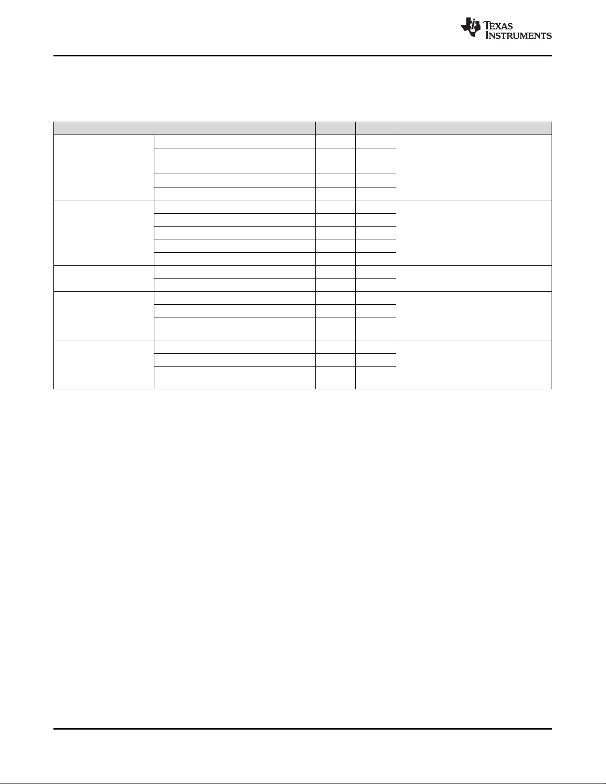
4.9 Frequency Synthesizer
All measurements were performed using the two-layer PCB CC1020EMX reference design. See Figure 6-1. The electrical
specifications given for 868 MHz are also applicable for 902 to 928 MHz. TA= 25°C, AVDD = DVDD = 3.0 V,
fC= 14.7456 MHz if nothing else stated.
PARAMETER TYP UNIT CONDITION
At 12.5 kHz offset from carrier –90 dBc/Hz
Phase noise, Measured using loop filter components
402 to 470 MHz At 50 kHz offset from carrier –105 dBc/Hz given in Table 6-2. The phase noise will
12.5 kHz channel spacing be higher for larger PLL loop filter
Phase noise, Measured using loop filter components
804 to 960 MHz At 50 kHz offset from carrier –101 dBc/Hz given in Table 6-2. The phase noise will
25 kHz channel spacing be higher for larger PLL loop filter
PLL loop bandwidth
PLL lock time
(RX / TX turn time)
PLL turn-on time.
From power down mode
with crystal oscillator
running.
At 25 kHz offset from carrier –100 dBc/Hz
At 100 kHz offset from carrier –110 dBc/Hz
At 1 MHz offset from carrier –114 dBc/Hz
At 12.5 kHz offset from carrier –85 dBc/Hz
At 25 kHz offset from carrier –95 dBc/Hz
At 100 kHz offset from carrier –109 dBc/Hz
At 1 MHz offset from carrier –118 dBc/Hz
12.5 kHz channel spacing, 433 MHz 2.7 kHz
25 kHz channel spacing, 868 MHz 8.3 kHz
12.5 kHz channel spacing, 433 MHz 900 µs 307.2 kHz frequency step to RF frequency
25 kHz channel spacing, 868 MHz 640 µs
500 kHz channel spacing 14 µs
12.5 kHz channel spacing, 433 MHz 3.2 ms Time from writing to registers to RF
25 kHz channel spacing, 868 MHz 2.5 ms
500 kHz channel spacing 700 µs
Unmodulated carrier.
bandwidth.
Unmodulated carrier.
bandwidth.
After PLL and VCO calibration. The PLL
loop bandwidth is programmable.
within ±10% of channel spacing. Depends
on loop filter component values and
PLL_BW register setting. See Table 5-13
for more details.
frequency within ±10% of channel
spacing. Depends on loop filter
component values and PLL_BW register
setting. See Table 5-12 for more details.
14 Specifications Copyright © 2006–2015, Texas Instruments Incorporated
Submit Documentation Feedback
Product Folder Links: CC1020
Page 15
CC1020
www.ti.com
SWRS046H –NOVEMBER 2006–REVISED MARCH 2015
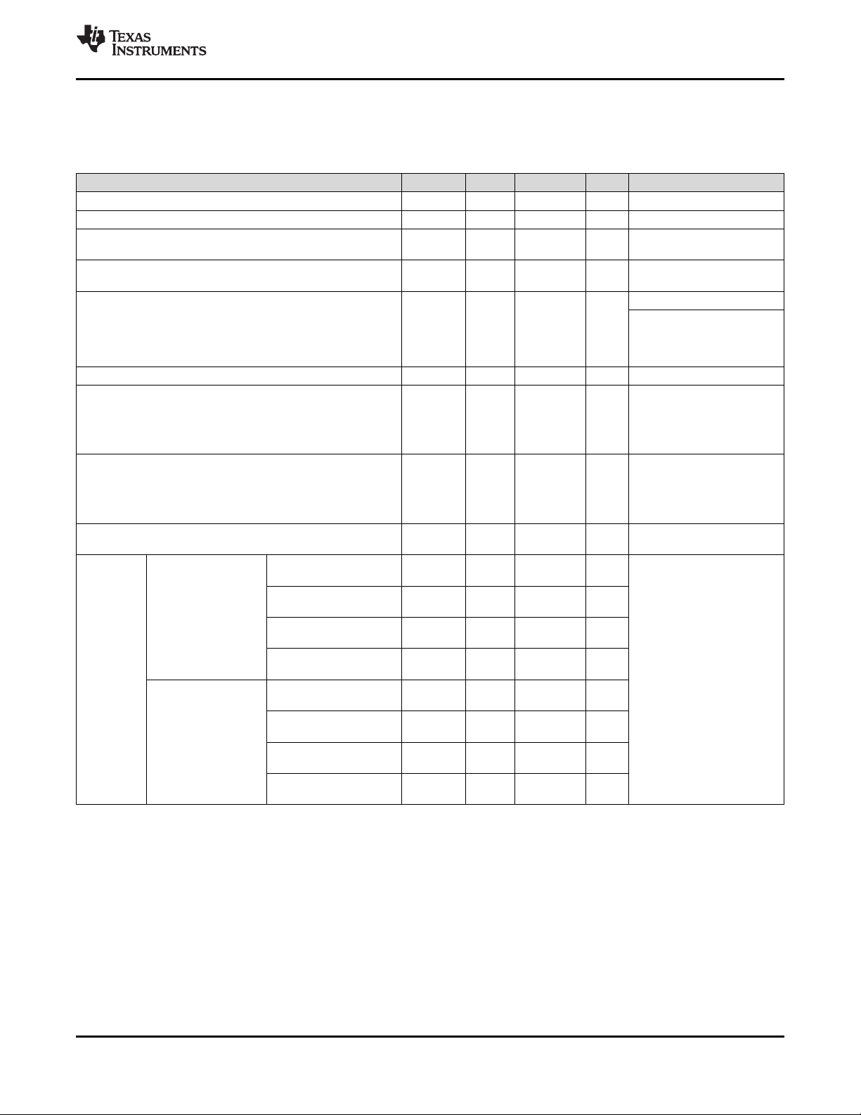
4.10 Digital Inputs and Outputs
All measurements were performed using the two-layer PCB CC1020EMX reference design. See Figure 6-1. The electrical
specifications given for 868 MHz are also applicable for 902 to 928 MHz. TA= 25°C, AVDD = DVDD = 3.0 V,
fC= 14.7456 MHz if nothing else stated.
PARAMETER MIN TYP MAX UNIT CONDITION
Logic "0" input voltage 0 0.3 × VDD V
Logic "1" input voltage 0.7 × VDD VDD V
Logic "0" output voltage 0 0.4 V
Logic "1" output voltage 2.5 VDD V
Logic “0” input current N/A –1 µA
Logic “1” input current N/A 1 µA Input signal equals VDD
DIO setup time 20 ns positive edge of DCLK. Data
DIO hold time 10 ns positive edge of DCLK. Data
Serial interface (PCLK, PDI, PDO and PSEL) timing See Table 5-1 for more
specification details
Pin drive,
LNA_EN,
PA_EN
Source current
Sink current
0 V on LNA_EN, PA_EN
pins
0.5 V on LNA_EN,
PA_EN pins
1.0 V on LNA_EN,
PA_EN pins
1.5 V on LNA_EN,
PA_EN pins
3.0 V on LNA_EN,
PA_EN pins
2.5 V on LNA_EN,
PA_EN pins
2.0 V on LNA_EN,
PA_EN pins
1.5 V on LNA_EN,
PA_EN pins
0.90 mA
0.87 mA
0.81 mA
0.69 mA
0.93 mA
0.92 mA
0.89 mA
0.79 mA
Output current –2.0 mA,
3.0-V supply voltage
Output current 2.0 mA,
3.0-V supply voltage
Input signal equals GND.
PSEL has an internal pullup
resistor and during
configuration the current will
be –350 µA.
TX mode, minimum time DIO
must be ready before the
should be set up on the
negative edge of DCLK.
TX mode, minimum time DIO
must be held after the
should be set up on the
negative edge of DCLK.
See Figure 5-32 for more
details.
Copyright © 2006–2015, Texas Instruments Incorporated Specifications 15
Submit Documentation Feedback
Product Folder Links: CC1020
Page 16
CC1020
SWRS046H –NOVEMBER 2006–REVISED MARCH 2015
www.ti.com
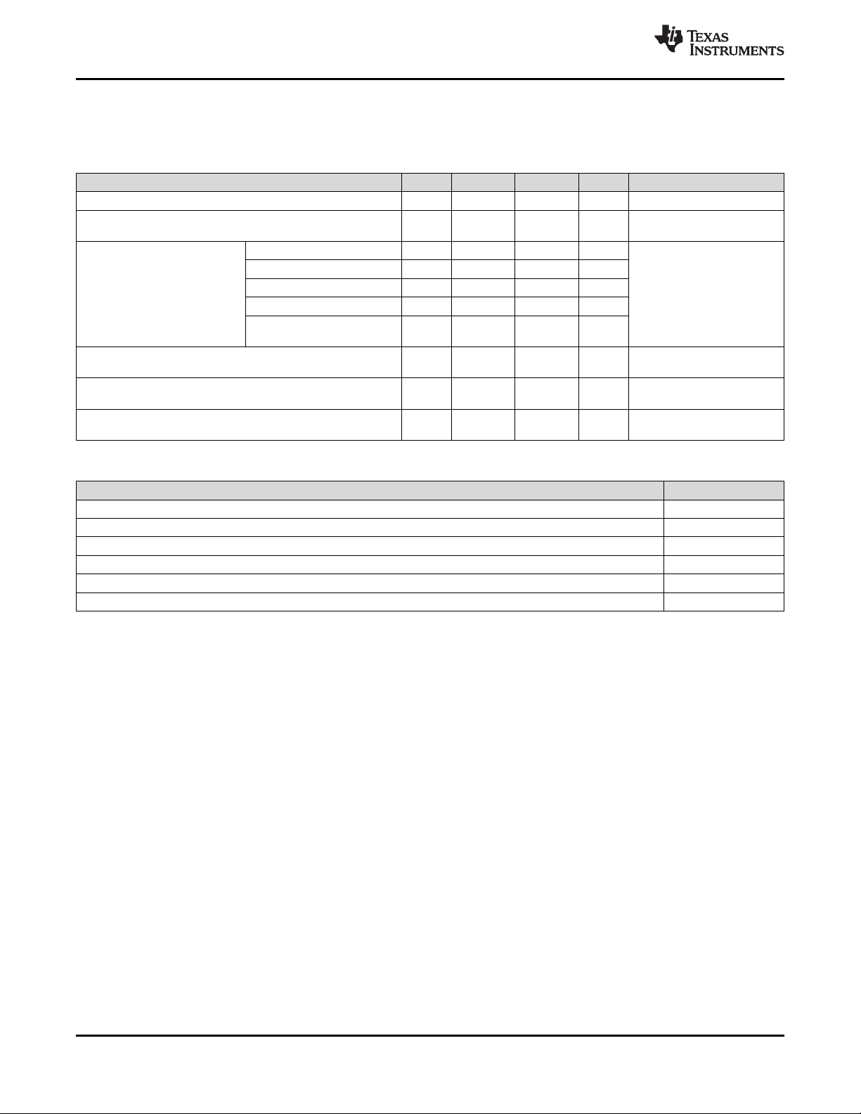
4.11 Current Consumption
All measurements were performed using the two-layer PCB CC1020EMX reference design. See Figure 6-1. The electrical
specifications given for 868 MHz are also applicable for 902 to 928 MHz. TA= 25°C, AVDD = DVDD = 3.0 V,
fC= 14.7456 MHz if nothing else stated.
PARAMETER MIN TYP MAX UNIT CONDITION
Power Down mode 0.2 1.8 µA Oscillator core off
Current Consumption,
receive mode 433 and 868 MHz
P = –20 dBm 12.3/14.5 mA
P = –5 dBm 14.4/17.0 mA
Current Consumption, P = 0 dBm 16.2/20.5 mA
transmit mode 433/868 MHz:
P = +5 dBm 20.5/25.1 mA
P = +10 dBm
(433 MHz only)
Current Consumption, crystal oscillator 77 µA
Current Consumption, crystal oscillator and bias 500 µA
Current Consumption, crystal oscillator, bias and synthesizer 7.5 mA
19.9 mA
The output power is
delivered to a 50 Ω singleended load.
See Section 5.10.2 for more
details.
27.1 mA
14.7456 MHz, 16 pF load
crystal
14.7456 MHz, 16 pF load
crystal
14.7456 MHz, 16 pF load
crystal
4.12 Thermal Resistance Characteristics for VQFNP Package
NAME DESCRIPTION °C/W
R
θJC(top)
R
θJB
R
θJA
Psi
JT
Psi
JB
R
θJC(bottom)
Junction-to-case (top) 16.2
Junction-to-board 6.9
Junction-to-free air 30.7
Junction-to-package top 0.2
Junction-to-board 6.9
Junction-to-case (bottom) 1.0
(1) °C/W = degrees Celsius per watt.
(2) These values are based on a JEDEC-defined 2S2P system (with the exception of the Theta JC [RθJC] value, which is based on a
JEDEC-defined 1S0P system) and will change based on environment as well as application. For more information, see these
EIA/JEDEC standards:
• JESD51-2, Integrated Circuits Thermal Test Method Environmental Conditions - Natural Convection (Still Air)
• JESD51-3, Low Effective Thermal Conductivity Test Board for Leaded Surface Mount Packages
• JESD51-7, High Effective Thermal Conductivity Test Board for Leaded Surface Mount Packages
• JESD51-9, Test Boards for Area Array Surface Mount Package Thermal Measurements
Power dissipation of 2 W and an ambient temperature of 70ºC is assumed.
(1) (2)
16 Specifications Copyright © 2006–2015, Texas Instruments Incorporated
Submit Documentation Feedback
Product Folder Links: CC1020
Page 17
RF_IN
LNA
FREQ
SYNTH
DIGITAL
DEMODULATOR
- Digital RSSI
- Gain Control
- Image Suppression
- Channel Filtering
- Demodulation
DIGITAL
MODULATOR
- Modulation
- Data shaping
- Power Control
BIAS
Power
Control
DIGITAL
INTERFACE
TO mC
CONTROL
LOGIC
PA
ADC
ADC
RF_OUT
R_BIAS
XOSC_Q1 XOSC_Q2
PDO
XOSC
VC
CHP_OUT
LNA 2
0
90
:2
0
90
:2
Multiplexer
Multiplexer
PA_EN
LNA_EN
PCLK
PDI
PSEL
www.ti.com
5 Detailed Description
5.1 Overview
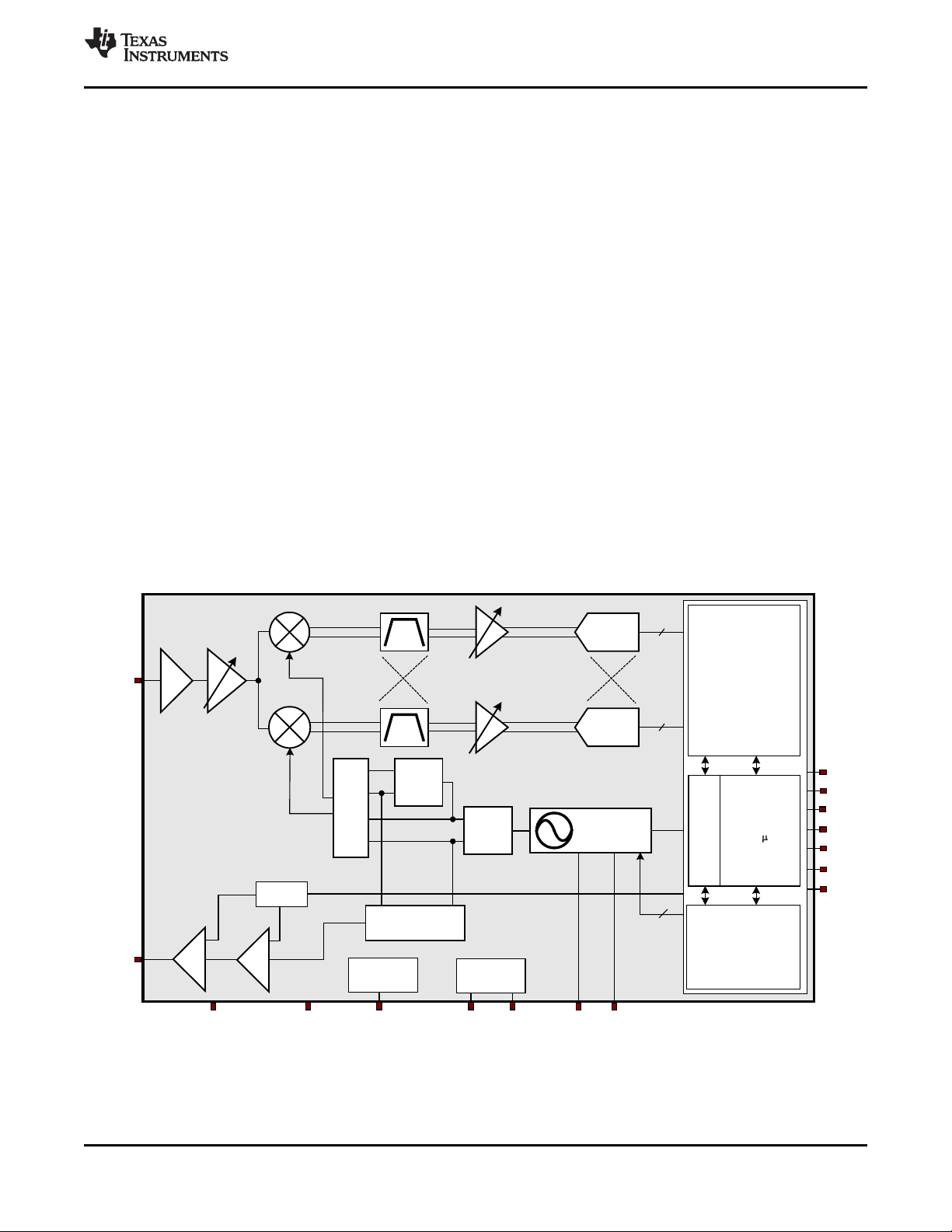
A simplified block diagram of CC1020 is shown in Figure 5-1. Only signal pins are shown.
CC1020 features a low-IF receiver. The received RF signal is amplified by the low-noise amplifier (LNA
and LNA2) and down-converted in quadrature (I and Q) to the intermediate frequency (IF). At IF, the I/Q
signal is complex filtered and amplified, and then digitized by the ADCs. Automatic gain control, fine
channel filtering, demodulation and bit synchronization is performed digitally. CC1020 outputs the digital
demodulated data on the DIO pin. A synchronized data clock is available at the DCLK pin. RSSI is
available in digital format and can be read via the serial interface. The RSSI also features a programmable
carrier sense indicator.
In transmit mode, the synthesized RF frequency is fed directly to the power amplifier (PA). The RF output
is frequency shift keyed (FSK) by the digital bit stream that is fed to the DIO pin. Optionally, a Gaussian
filter can be used to obtain Gaussian FSK (GFSK).
The frequency synthesizer includes a completely on-chip LC VCO and a 90 degrees phase splitter for
generating the LO_I and LO_Q signals to the down-conversion mixers in receive mode. The VCO
operates in the frequency range 1.608 to 1.880 GHz. The CHP_OUT pin is the charge pump output and
VC is the control node of the on-chip VCO. The external loop filter is placed between these pins. A crystal
is to be connected between XOSC_Q1 and XOSC_Q2. A lock signal is available from the PLL.
CC1020
SWRS046H –NOVEMBER 2006–REVISED MARCH 2015
The 4-wire SPI serial interface is used for configuration.
5.2 Functional Block Diagram
Figure 5-1. CC1020 Simplified Block Diagram
Copyright © 2006–2015, Texas Instruments Incorporated Detailed Description 17
Submit Documentation Feedback
Product Folder Links: CC1020
Page 18
CC1020
SWRS046H –NOVEMBER 2006–REVISED MARCH 2015
5.3 Configuration Overview
CC1020 can be configured to achieve optimum performance for different applications. Through the
programmable configuration registers the following key parameters can be programmed:
• Receive and transmit mode
• RF output power
• Frequency synthesizer key parameters:
– RF output frequency
– FSK frequency separation
– Crystal oscillator reference frequency
• Power-down and power-up mode
• Power-down and power-up mode
• Data rate and data format (NRZ, Manchester coded or UART interface)
• Synthesizer lock indicator mode
• Digital RSSI and carrier sense
• FSK, GFSK, and OOK modulation
5.3.1 Configuration Software
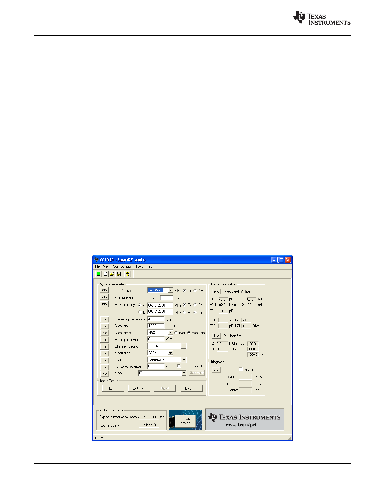
TI provides users of CC1020 with a software program, SmartRF Studio (Windows interface) that
generates all necessary CC1020 configuration data based on the user’s selections of various parameters.
These hexadecimal numbers will then be the necessary input to the microcontroller for the configuration of
CC1020. In addition, the program will provide the user with the component values needed for the
input/output matching circuit, the PLL loop filter and the LC filter.
www.ti.com
Figure 5-2 shows the user interface of the CC1020 configuration software.
Figure 5-2. SmartRF™ Studio user interface
18 Detailed Description Copyright © 2006–2015, Texas Instruments Incorporated
Submit Documentation Feedback
Product Folder Links: CC1020
Page 19

www.ti.com
5.4 Microcontroller Interface
Used in a typical system, CC1020 will interface to a microcontroller. This microcontroller must be able to:
• Program CC1020 into different modes via the 4-wire serial configuration interface (PDI, PDO, PCLK
and PSEL).
• Interface to the bi-directional synchronous data signal interface (DIO and DCLK).
• Optionally, the microcontroller can do data encoding and decoding.
• Optionally, the microcontroller can monitor the LOCK pin for frequency lock status, carrier sense status
or other status information.
• Optionally, the microcontroller can read back the digital RSSI value and other status information via the
4-wire serial interface.
5.4.1 Configuration Interface
The microcontroller interface is shown in Figure 5-3. The microcontroller uses 3 or 4 I/O pins for the
configuration interface (PDI, PDO, PCLK and PSEL). PDO should be connected to a microcontroller input.
PDI, PCLK and PSEL must be microcontroller outputs. One I/O pin can be saved if PDI and PDO are
connected together and a bi-directional pin is used at the microcontroller.
The microcontroller pins connected to PDI, PDO and PCLK can be used for other purposes when the
configuration interface is not used. PDI, PDO and PCLK are high impedance inputs as long as PSEL is
not activated (active low).
CC1020
SWRS046H –NOVEMBER 2006–REVISED MARCH 2015
PSEL has an internal pullup resistor and should be left open (tri-stated by the microcontroller) or set to a
high level during power down mode in order to prevent a trickle current flowing in the pullup.
5.4.2 Signal Interface
A bi-directional pin is usually used for data (DIO) to be transmitted and data received. DCLK providing the
data timing should
As an option, the data output in receive mode can be made available on a separate pin. See Section 5.6
for further details.
5.4.3 PLL Lock Signal
Optionally, one microcontroller pin can be used to monitor the LOCK signal. This signal is at low logic
level when the PLL is in lock. It can also be used for carrier sense and to monitor other internal test
signals.
Figure 5-3. Microcontroller Interface
Copyright © 2006–2015, Texas Instruments Incorporated Detailed Description 19
Submit Documentation Feedback
Product Folder Links: CC1020
Page 20

PDI
Address Write mode
6 5 4 3 2 1 0
7
6
5 4
3
2 1
0
Data byte
T
HD
T
SS
T
CL,min
T
CH,min
T
HS
W
T
SD
PDO
CC1020
SWRS046H –NOVEMBER 2006–REVISED MARCH 2015
5.5 4-wire Serial Configuration Interface
CC1020 is configured via a simple 4-wire SPI-compatible interface (PDI, PDO, PCLK and PSEL) where
CC1020 is the slave. There are 8-bit configuration registers, each addressed by a 7-bit address. A
Read/Write bit initiates a read or write operation. A full configuration of CC1020 requires sending 33 data
frames of 16 bits each (7 address bits, R/W bit and 8 data bits). The time needed for a full configuration
depends on the PCLK frequency. With a PCLK frequency of 10 MHz the full configuration is done in less
than 53 ms. Setting the device in power down mode requires sending one frame only and will in this case
take less than 2 ms. All registers are also readable.
During each write-cycle, 16 bits are sent on the PDI-line. The seven most significant bits of each data
frame (A6:0) are the address-bits. A6 is the MSB (Most Significant Bit) of the address and is sent as the
first bit. The next bit is the R/W bit (high for write, low for read). The 8 data-bits are then transferred
(D7:0). During address and data transfer the PSEL (Program Select) must be kept low. See Figure 5-4.
The timing for the programming is also shown in Figure 5-4 with reference to Table 5-1. The clocking of
the data on PDI is done on the positive edge of PCLK. Data should be set up on the negative edge of
PCLK by the microcontroller. When the last bit, D0, of the 8 data-bits has been loaded, the data word is
loaded into the internal configuration register.
The configuration data will be retained during a programmed power down mode, but not when the power
supply is turned off. The registers can be programmed in any order.
The configuration registers can also be read by the microcontroller via the same configuration interface.
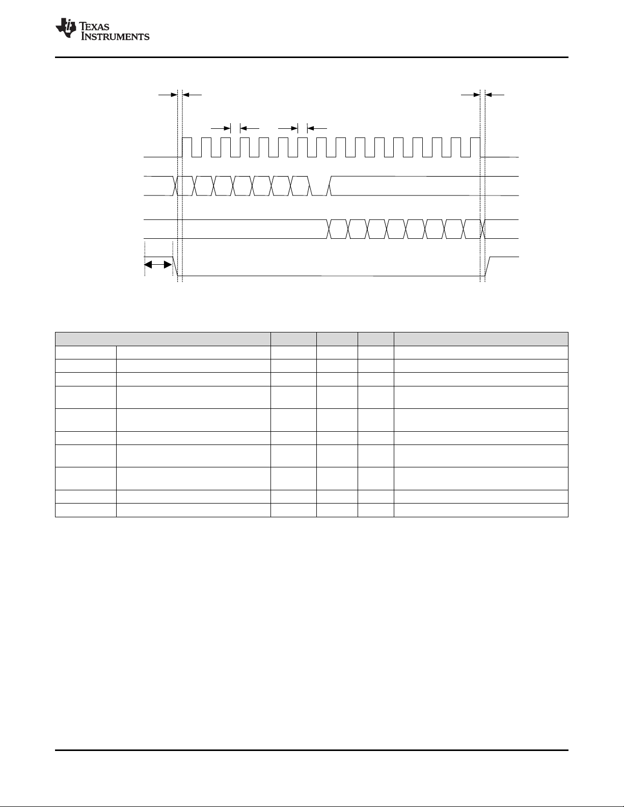
The seven address bits are sent first, then the R/W bit set low to initiate the data read-back. CC1020 then
returns the data from the addressed register. PDO is used as the data output and must be configured as
an input by the microcontroller. The PDO is set at the negative edge of PCLK and should be sampled at
the positive edge. The read operation is illustrated in Figure 5-5.
www.ti.com
PSEL must be set high between each read/write operation.
Figure 5-4. Configuration Registers Write Operation
20 Detailed Description Copyright © 2006–2015, Texas Instruments Incorporated
Submit Documentation Feedback
Product Folder Links: CC1020
Page 21
PDI
Address Read mode
6 5 4 3 2 1 0
T
SS
T
CL,min
T
CH,min
T
HS
R
PDO
7
6
5 4
3 2
1
0
Data byte
T
SH
www.ti.com
CC1020
SWRS046H –NOVEMBER 2006–REVISED MARCH 2015
Figure 5-5. Configuration Registers Read Operation
Table 5-1. Serial Interface, Timing Specification
(1)
PARAMETER MIN MAX UNIT CONDITION
F
PCLK
T
CL,min
T
CH,min
T
T
T
T
T
T
T
SS
HS
SH
SD
HD
rise
fall
PCLK, clock frequency 10 MHz
PCLK low pulse duration 50 ns The minimum time PCLK must be low.
PCLK high pulse duration 50 ns The minimum time PCLK must be high.
PSEL setup time 25 ns
PSEL hold time 25 ns
The minimum time PSEL must be low before
positive edge of PCLK.
The minimum time PSEL must be held low
after the negative edge of PCLK.
PSEL high time 50 ns The minimum time PSEL must be high.
PDI setup time 25 ns
PDI hold time 25 ns
The minimum time data on PDI must be ready
before the positive edge of PCLK.
The minimum time data must be held at PDI,
after the positive edge of PCLK.
Rise time 100 ns The maximum rise time for PCLK and PSEL
Fall time 100 ns The maximum fall time for PCLK and PSEL
(1) The setup and hold times refer to 50% of VDD. The rise and fall times refer to 10% / 90% of VDD. The maximum load that this table is
valid for is 20 pF.
5.6 Signal Interface
The CC1020 can be used with NRZ (Non-Return-to-Zero) data or Manchester (also known as bi-phaselevel) encoded data. CC1020 can also synchronize the data from the demodulator and provide the data
clock at DCLK. The data format is controlled by the DATA_FORMAT[1:0] bits in the MODEM register.
CC1020 can be configured for three different data formats: Synchronous NRZ mode, Transparent
Asynchronous UART mode, and Synchronous Manchester encoded mode.
Copyright © 2006–2015, Texas Instruments Incorporated Detailed Description 21
Submit Documentation Feedback
Product Folder Links: CC1020
Page 22

CC1020
SWRS046H –NOVEMBER 2006–REVISED MARCH 2015
5.6.1 Synchronous NRZ Mode
In transmit mode CC1020 provides the data clock at DCLK and DIO is used as data input. Data is clocked
into CC1020 at the rising edge of DCLK. The data is modulated at RF without encoding.
In receive mode CC1020 performs the synchronization and provides received data clock at DCLK and
data at DIO. The data should be clocked into the interfacing circuit at the rising edge of DCLK. See
Figure 5-6.
5.6.2 Transparent Asynchronous UART Mode
In transmit mode DIO is used as data input. The data is modulated at RF without synchronization or
encoding.
In receive mode the raw data signal from the demodulator is sent to the output (DIO). No synchronization
or decoding of the signal is done in CC1020 and should be done by the interfacing circuit.
If SEP_DI_DO = 0 in the INTERFACE register, the DIO pin is the data output in receive mode and data
input in transmit mode. The DCLK pin is not active and can be set to a high or low level by
DATA_FORMAT[0].
If SEP_DI_DO = 1 in the INTERFACE register, the DCLK pin is the data output in receive mode and the
DIO pin is the data input in transmit mode. In TX mode the DCLK pin is not active and can be set to a high
or low level by DATA_FORMAT[0]. See Figure 5-7.
www.ti.com
5.6.3 Synchronous Manchester Encoded Mode
In transmit mode CC1020 provides the data clock at DCLK and DIO is used as data input. Data is clocked
into CC1020 at the rising edge of DCLK and should be in NRZ format. The data is modulated at RF with
Manchester code. The encoding is done by CC1020. In this mode the effective bit rate is half the baud
rate due to the coding. As an example, 4.8 kBaud Manchester encoded data corresponds to 2.4 kbps.
In receive mode CC1020 performs the synchronization and provides received data clock at DCLK and
data at DIO. CC1020 performs the decoding and NRZ data is presented at DIO. The data should be
clocked into the interfacing circuit at the rising edge of DCLK. See Figure 5-7.
In synchronous NRZ or Manchester mode the DCLK signal runs continuously both in RX and TX unless
the DCLK signal is gated with the carrier sense signal or the PLL lock signal. Refer to Section 5.18 and
Section 5.18.2 for more details.
If SEP_DI_DO = 0 in the INTERFACE register, the DIO pin is the data output in receive mode and data
input in transmit mode.
As an option, the data output can be made available at a separate pin. This is done by setting
SEP_DI_DO = 1 in the INTERFACE register. Then, the LOCK pin will be used as data output in
synchronous mode, overriding other use of the LOCK pin.
5.6.3.1 Manchester Encoding and Decoding
In the Synchronous Manchester encoded mode CC1020 uses Manchester coding when modulating the
data. The CC1020 also performs the data decoding and synchronization. The Manchester code is based
on transitions; a “0” is encoded as a low-to-high transition, a “1” is encoded as a high-to-low transition.
See Figure 5-9.
The Manchester code ensures that the signal has a constant DC component, which is necessary in some
FSK demodulators. Using this mode also ensures compatibility with CC400/CC900 designs.
22 Detailed Description Copyright © 2006–2015, Texas Instruments Incorporated
Submit Documentation Feedback
Product Folder Links: CC1020
Page 23

Clock provided by CC1020
FSK modulating signal (Manchester
encoded), internal in CC1020
Data provided by microcontroller
Clock provided by CC1020
Demodulated signal (Manchester
encoded), internal in CC1020
Data provided by CC1020
Clock provided by CC1020
FSK modulating signal (Manchester
encoded), internal in CC1020
Data provided by microcontroller
Clock provided by CC1020
Demodulated signal (Manchester
encoded), internal in CC1020
Data provided by CC1020
Clock provided by CC1020
FSK modulating signal (NRZ),
internal in CC1020
Data provided by microcontroller
Clock provided by CC1020
Demodulated signal (NRZ),
internal in CC1020
Data provided by CC1020
Clock provided by CC1020
FSK modulating signal (NRZ),
internal in CC1020
Data provided by microcontroller
Clock provided by CC1020
Demodulated signal (NRZ),
internal in CC1020
Data provided by CC1020
www.ti.com
CC1020
SWRS046H –NOVEMBER 2006–REVISED MARCH 2015
Figure 5-6. Synchronous NRZ Mode (SEP_DI_DO = 0)
Figure 5-7. Synchronous Manchester Encoded Mode (SEP_DI_DO = 0)
Copyright © 2006–2015, Texas Instruments Incorporated Detailed Description 23
Submit Documentation Feedback
Product Folder Links: CC1020
Page 24

xosc
f
8 (REF _ DIV 1) DIV1 DIV2
=
´ + ´ ´
Time
1 0 1 1 0 0 0 1 1 0 1
Time
1 0 1 1 0 0 0 1 1 0 1
DCLK is not used in transmit mode, and is
used as data output in receive mode. It can be
set to default high or low in transmit mode.
FSK modulating signal,
internal in CC1020
Data provided by UART (TXD)
DCLK is used as data output
provided by CC1020.
Connect to UART (RXD)
Demodulated signal (NRZ),
internal in CC1020
DIO is not used in receive mode. Used only
as data input in transmit mode
DCLK is not used in transmit mode, and is
used as data output in receive mode. It can be
set to default high or low in transmit mode.
FSK modulating signal,
internal in CC1020
Data provided by UART (TXD)
DCLK is used as data output
provided by CC1020.
Connect to UART (RXD)
Demodulated signal (NRZ),
internal in CC1020
DIO is not used in receive mode. Used only
as data input in transmit mode
CC1020
SWRS046H –NOVEMBER 2006–REVISED MARCH 2015
Figure 5-8. Transparent Asynchronous UART Mode (SEP_DI_DO = 1)
www.ti.com
5.7 Data Rate Programming
The data rate (baud rate) is programmable and depends on the crystal frequency and the programming of
the CLOCK (CLOCK_A and CLOCK_B) registers.
The baud rate (B.R.) is given by Equation 1.
Where:
DIV1 and DIV2 are given by the value of MCLK_DIV1 and MCLK_DIV2.
Table 5-4 shows some possible data rates as a function of crystal frequency in synchronous mode. In
asynchronous transparent UART mode any data rate up to 153.6 kBaud can be used.
Table 5-2. DIV2 for Different Settings of MCLK_DIV2
Figure 5-9. Manchester Encoding
MCLK_DIV2[1:0] DIV2
00 1
01 2
10 4
11 8
(1)
24 Detailed Description Copyright © 2006–2015, Texas Instruments Incorporated
Submit Documentation Feedback
Product Folder Links: CC1020
Page 25

www.ti.com
CC1020
SWRS046H –NOVEMBER 2006–REVISED MARCH 2015
Table 5-3. DIV1 for Different Settings of MCLK_DIV1
MCLK_DIV1[2:0] DIV1
000 2.5
001 3
010 4
011 7.5
100 12.5
101 40
110 48
111 64
Table 5-4. Some Possible Data Rates Versus Crystal Frequency
DATA RATE
[kBaud]
0.45 X X
0.5 X
0.6 X X X X X X X
0.9 X X
1 X
1.2 X X X X X X X
1.8 X X
2 X
2.4 X X X X X X X
3.6 X X
4 X
4.096 X X
4.8 X X X X X X X
7.2 X X
8 X
8.192 X X
9.6 X X X X X X X
14.4 X X
16 X
16.384 X X
19.2 X X X X X X X
28.8 X X
32 X
32.768 X X
38.4 X X X X X X X
57.6 X X
64 X
65.536 X
76.8 X X X X X X X
115.2 X X
128 X
153.6 X X X X X
4.9152 7.3728 9.8304 12.288 14.7456 17.2032 19.6608
CRYSTAL FREQUENCY [MHz]
Copyright © 2006–2015, Texas Instruments Incorporated Detailed Description 25
Submit Documentation Feedback
Product Folder Links: CC1020
Page 26
(TXDEV _ X 15)
dev ref
-
= ´ ´
(TXDEV _ X 16)
dev ref
-
= ´ ´
[ ]
c
ref
f
512
³ >
[ ]
c
ref
f
256
³ >
xosc
ref
f
REF _DIV 1=+
c ref
3 FREQ 0.5 DITHER
2 16384
+ ´
æ ö
= ´ +
ç ÷
è ø
c ref
3 FREQ 0.5 DITHER
4 32768
+ ´
æ ö
= ´ +
ç ÷
è ø
CC1020
SWRS046H –NOVEMBER 2006–REVISED MARCH 2015
5.8 Frequency Programming
Programming the frequency word in the configuration registers sets the operation frequency. There are
two frequency words registers, termed FREQ_A and FREQ_B, which can be programmed to two different
frequencies. One of the frequency words can be used for RX (local oscillator frequency) and the other for
TX (transmitting carrier frequency) in order to be able to switch very fast between RX mode and TX mode.
They can also be used for RX (or TX) at two different channels. The F_REG bit in the MAIN register
selects frequency word A or B.
The frequency word is located in FREQ_2A:FREQ_1A:FREQ_0A and FREQ_2B:FREQ_1B:FREQ_0B for
the FREQ_A and FREQ_B word respectively. The LSB of the FREQ_0 registers are used to enable
dithering, see Section 5.8.1.
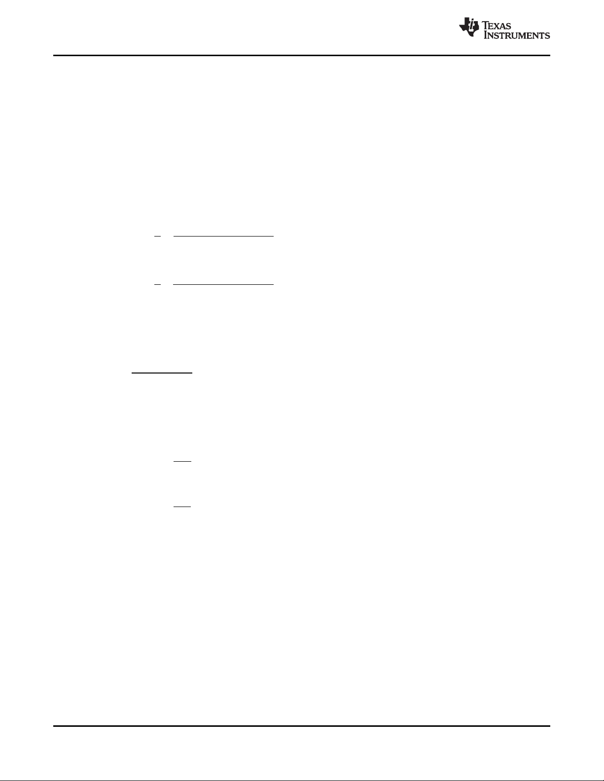
The PLL output frequency is given by Equation 2 in the frequency band 402 to 470 MHz.
The PLL output frequency is given by Equation 3 in the frequency band 804 to 960 MHz.
The BANDSELECT bit in the ANALOG register controls the frequency band used. BANDSELECT = 0
gives 402 to 470 MHz, and BANDSELECT = 1 gives 804 to 960 MHz.
www.ti.com
(2)
(3)
The reference frequency is the crystal oscillator clock frequency divided by REF_DIV (3 bits in the
CLOCK_A or CLOCK_B register), a number between 1 and 7, as shown in Equation 4.
(4)
FSK frequency deviation is programmed in the DEVIATION register. The deviation programming is divided
into a mantissa (TXDEV_M[3:0]) and an exponent (TXDEV_X[2:0]).
Generally REF_DIV should be as low as possible but the requirements (shown in Equation 5 and
Equation 6) must be met.
(5)
Equation 5 in the frequency band 402 to 470 MHz, and Equation 6 in the frequency band 804 to 960 MHz.
(6)
The PLL output frequency Equation 2 and Equation 3 give the carrier frequency, fc, in transmit mode
(centre frequency). The two FSK modulation frequencies are given by Equation 7 and Equation 7.
f0= fc– f
f1= fc+ f
dev
dev
(7)
(8)
Where:
f
is set by the DEVIATION register shown in Equation 9 in the frequency band 402 to 470 MHz and
dev
in Equation 10 in the frequency band 804 to 960 MHz.
26 Detailed Description Copyright © 2006–2015, Texas Instruments Incorporated
OOK (On-Off Keying) is used if TXDEV_M[3:0] = 0000.
The TX_SHAPING bit in the DEVIATION register controls Gaussian shaping of the modulation signal.
Submit Documentation Feedback
Product Folder Links: CC1020
(9)
(10)
Page 27

[ ]
xoscx
IF
f
8 (ADC _DIV 2 : 0 1)
=
´ +
www.ti.com
In receive mode the frequency must be programmed to be the LO frequency. Low side LO injection is
used, hence Equation 8.
fLO= fc– f
IF
Where:
fIFis the IF frequency (ideally 307.2 kHz).
5.8.1 Dithering
Spurious signals will occur at certain frequencies depending on the division ratios in the PLL. To reduce
the strength of these spurs, a common technique is to use a dithering signal in the control of the frequency
dividers. Dithering is activated by setting the DITHER bit in the FREQ_0 registers. It is recommended to
use the dithering in order to achieve the best possible performance.
5.9 Receiver
5.9.1 IF Frequency
The IF frequency is derived from the crystal frequency as shown in Equation 12.
CC1020
SWRS046H –NOVEMBER 2006–REVISED MARCH 2015
(11)
(12)
Where:
ADC_DIV[2:0] is set in the MODEM register.
The analog filter succeeding the mixer is used for wideband and anti-alias filtering, which is important for
the blocking performance at 1 MHz and larger offsets. This filter is fixed and centered on the nominal IF
frequency of 307.2 kHz. The bandwidth of the analog filter is about 160 kHz.
Using crystal frequencies which gives an IF frequency within 300 to 320 kHz means that the analog filter
can be used (assuming low frequency deviations and low data rates).
Large offsets, however, from the nominal IF frequency will give an un-symmetric filtering (variation in
group delay and different attenuation) of the signal, resulting in decreased sensitivity and selectivity. See
AN022 CC1020 Crystal Frequency Selection (SWRA070) for more details.
For IF frequencies other than 300 to 320 kHz and for high frequency deviation and high data rates
(typically ≥ 76.8 kBaud) the analog filter must be bypassed by setting FILTER_BYPASS = 1 in the FILTER
register. In this case the blocking performance at 1 MHz and larger offsets will be degraded.
The IF frequency is always the ADC clock frequency divided by 4. The ADC clock frequency should
therefore be as close to 1.2288 MHz as possible.
5.9.2 Receiver Channel Filter Bandwidth
In order to meet different channel spacing requirements, the receiver channel filter bandwidth is
programmable. It can be programmed from 9.6 to 307.2 kHz.
The minimum receiver channel filter bandwidth depends on baud rate, frequency separation and crystal
tolerance.
The signal bandwidth must be smaller than the available receiver channel filter bandwidth. The signal
bandwidth (SBW) can be approximated by (Carson’s rule) shown in Equation 13.
Where:
Copyright © 2006–2015, Texas Instruments Incorporated Detailed Description 27
SBW = 2 × fm+ 2 × frequency deviation (13)
fmis the modulating signal.
Submit Documentation Feedback
Product Folder Links: CC1020
Page 28
[ ]
307.2
(DEC _ DIV 1) kHz
=
+
CC1020
SWRS046H –NOVEMBER 2006–REVISED MARCH 2015
In Manchester mode the maximum modulating signal occurs when transmitting a continuous sequence of
0s (or 1s). In NRZ mode the maximum modulating signal occurs when transmitting a 0-1-0 sequence. In
both Manchester and NRZ mode 2 × fm is then equal to the programmed baud rate. The equation for
SBW can then be rewritten as shown in Equation 14.
SBW = Baud rate + frequency separation (14)
Furthermore, the frequency offset of the transmitter and receiver must also be considered. Assuming
equal frequency error in the transmitter and receiver (same type of crystal) the total frequency error is
shown in Equation 15.
f_error = ±2 × XTAL_ppm × f_RF (15)
Where:
XTAL_ppm is the total accuracy of the crystal including initial tolerance, temperature drift, loading and
ageing.
F_RF is the RF operating frequency.
The minimum receiver channel filter bandwidth (ChBW) can then be estimated as shown in Equation 16.
ChBW > SBW + 2 × f_error (16)
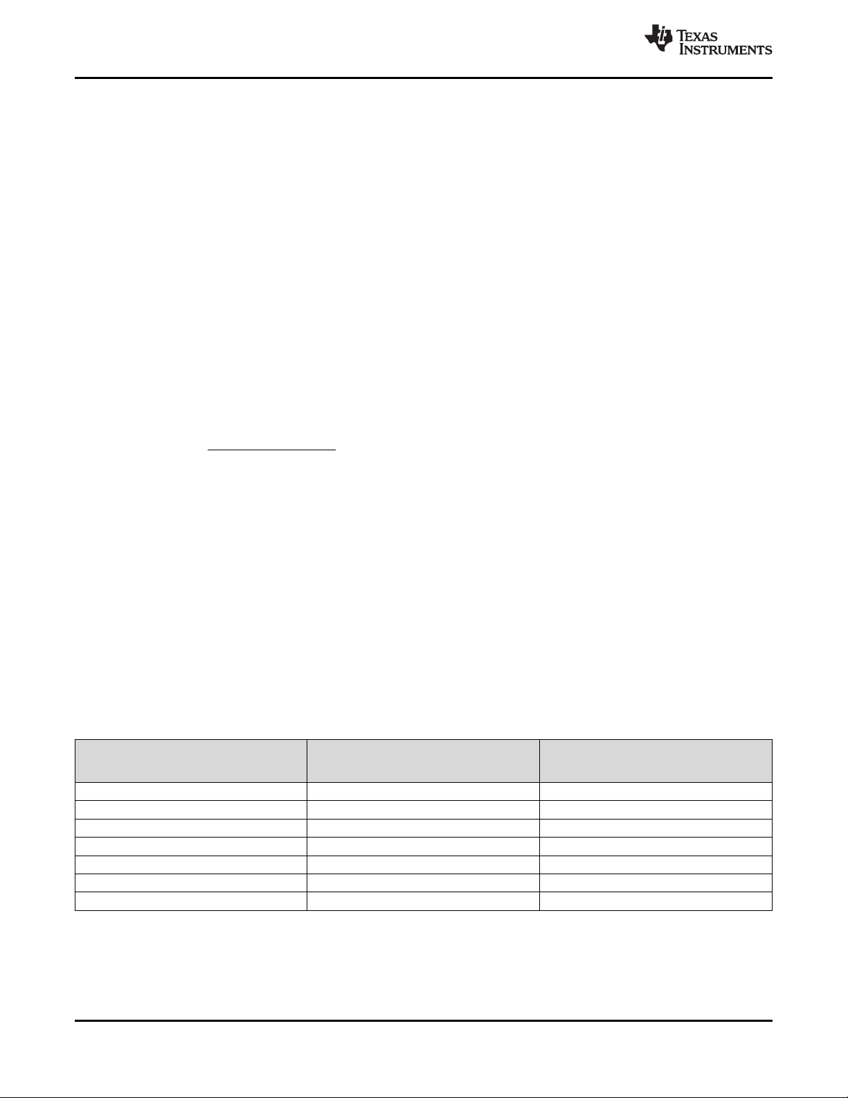
The DEC_DIV[4:0] bits in the FILTER register control the receiver channel filter bandwidth. The 6 dB
bandwidth is given by Equation 17.
www.ti.com
Where:
the IF frequency is set to 307.2 kHz.
In SmartRF Studio the user specifies the channel spacing and the channel filter bandwidth is set
according to Table 5-5.
For narrowband systems with channel spacings of 12.5 and 25 kHz the channel filter bandwidth is 12.288
kHz and 19.2 kHz respectively to comply with ARIB STD-T67 and EN 300 220.
For wideband systems (channel spacing of 50 kHz and above) it is possible to use different channel filter
bandwidths than given in Table 5-5.
There is a trade-off between selectivity as well as sensitivity and accepted frequency tolerance. In
applications where larger frequency drift is expected, the filter bandwidth can be increased, but with
reduced adjacent channel rejection (ACR) and sensitivity.
Table 5-5. Channel Filter Bandwidths Used for the Channel Spacings Defined in SmartRF Studio
CHANNEL SPACING FILTER BANDWIDTH
[kHz] [kHz]
12.5 12.288 24 (11000b)
25 19.2 15 (01111b)
50 25.6 11 (01011b)
100 51.2 5 (00101b)
150 102.4 2 (00010b)
200 153.6 1 (00001b)
500 307.2 0 (00000b)
FILTER.DEC_DIV
[4:0]
[decimal(binary)]
(17)
28 Detailed Description Copyright © 2006–2015, Texas Instruments Incorporated
Submit Documentation Feedback
Product Folder Links: CC1020
Page 29

Bit synchronizer
and data decoder
Data slicer
comparator
Average filter
Decimator
Frequency
detector
Digital filtering
Data
filter
www.ti.com
5.9.3 Demodulator, Bit Synchronizer, and Data Decision
The block diagram for the demodulator, data slicer and bit synchronizer is shown in Figure 5-10. The builtin bit synchronizer synchronizes the internal clock to the incoming data and performs data decoding. The
data decision is done using over-sampling and digital filtering of the incoming signal. This improves the
reliability of the data transmission. Using the synchronous modes simplifies the data-decoding task
substantially.
The recommended preamble is a ‘010101…’ bit pattern. The same bit pattern should also be used in
Manchester mode, giving a ‘011001100110…‘chip’ pattern. This is necessary for the bit synchronizer to
synchronize to the coding correctly.
The data slicer does the bit decision. Ideally the two received FSK frequencies are placed symmetrically
around the IF frequency. However, if there is some frequency error between the transmitter and the
receiver, the bit decision level should be adjusted accordingly. In CC1020, this is done automatically by
measuring the two frequencies and use the average value as the decision level.
The digital data slicer in CC1020 uses an average value of the minimum and maximum frequency
deviation detected as the comparison level. The RXDEV_X[1:0] and RXDEV_M[3:0] in the
AFC_CONTROL register are used to set the expected deviation of the incoming signal. Once a shift in the
received frequency larger than the expected deviation is detected, a bit transition is recorded and the
average value to be used by the data slicer is calculated.
The minimum number of transitions required to calculate a slicing level is 3. That is, a 010 bit pattern
(NRZ).
CC1020
SWRS046H –NOVEMBER 2006–REVISED MARCH 2015
The actual number of bits used for the averaging can be increased for better data decision accuracy. This
is controlled by the SETTLING[1:0] bits in the AFC_CONTROL register. If RX data is present in the
channel when the RX chain is turned on, then the data slicing estimate will usually give correct results
after 3 bit transitions. The data slicing accuracy will increase after this, depending on the SETTLING[1:0]
bits. If the start of transmission occurs after the RX chain has turned on, the minimum number of bit
transitions (or preamble bits) before correct data slicing will depend on the SETTLING[1:0] bits.
The automatic data slicer average value function can be disabled by setting SETTLING[1:0] = 00. In this
case a symmetrical signal around the IF frequency is assumed.
The internally calculated average FSK frequency value gives a measure for the frequency offset of the
receiver compared to the transmitter. This information can also be used for an automatic frequency control
(AFC) as described in Section 5.9.13.
Figure 5-10. Demodulator Block Diagram
Copyright © 2006–2015, Texas Instruments Incorporated Detailed Description 29
Submit Documentation Feedback
Product Folder Links: CC1020
Page 30

CC1020
SWRS046H –NOVEMBER 2006–REVISED MARCH 2015
5.9.4 Receiver Sensitivity Versus Data Rate and Frequency Separation
The receiver sensitivity depends on the channel filter bandwidth, data rate, data format, FSK frequency
separation and the RF frequency. Typical figures for the receiver sensitivity (BER = 10–3) are shown in
Table 5-6 and Table 5-7 for FSK. For best performance, the frequency deviation should be at least half
the baud rate in FSK mode.
The sensitivity is measured using the matching network shown in the application circuit in Figure 6-1,
which includes an external T/R switch.
Refer to AN029 CC1020/1021 Automatic Frequency Control (AFC) (SWRA063) for plots of sensitivity
versus frequency offset.
Table 5-6. Typical Receiver Sensitivity as a Function of Data Rate at 433 MHz, FSK Modulation,
BER = 10–3, Pseudo-random Data (PN9 Sequence)
www.ti.com
DATA RATE DEVIATION
[kBaud] [kHz]
2.4 optimized
sensitivity
2.4 optimized
selectivity
(1) Optimized selectivity is relevant for systems targeting compliance with ARIB STD-T67, 12.5 kHz channel spacing.
(1)
(1)
4.8 25 ±2.475 19.2 –112 –112 –112
9.6 50 ±4.95 25.6 –110 –111 –110
19.2 100 ±9.9 51.2 –107 –108 –107
38.4 150 ±19.8 102.4 –104 –104 –104
76.8 200 ±36.0 153.6 –101 –101 –101
153.6 500 ±72.0 307.2 –96 –97 –96
CHANNEL
SPACING FILTER BW
[kHz]
12.5 ±2.025 9.6 –115 –118 –115
12.5 ±2.025 12.288 –112 –114 –112
NRZ MODE UART MODE
SENSITIVITY [dBm]
MANCHESTER
MODE
Table 5-7. Typical Receiver Sensitivity as a Function of Data Rate at 868 MHz, FSK Modulation,
BER = 10–3, Pseudo-random Data (PN9 Sequence)
DATA RATE
[kBaud]
2.4 12.5 ±2.025 12.288 –112 –116 –112
4.8 25 ±2.475 19.2 –111 –112 –111
9.6 50 ±4.95 25.6 –109 –110 –109
19.2 100 ±9.9 51.2 –107 –107 –107
38.4 150 ±19.8 102.4 –103 –103 –103
76.8 200 ±36.0 153.6 –99 –100 –99
153.6 500 ±72.0 307.2 –94 –94 –94
CHANNEL
SPACING DEVIATION [kHz] FILTER BW
[kHz]
NRZ MODE UART MODE
SENSITIVITY [dBm]
MANCHESTER
MODE
30 Detailed Description Copyright © 2006–2015, Texas Instruments Incorporated
Submit Documentation Feedback
Product Folder Links: CC1020
Page 31

filter _clock
RSSI
AGC _ AVG[1: 0] 1
f
2
+
=
www.ti.com
5.9.5 RSSI
CC1020 has a built-in RSSI (Received Signal Strength Indicator) giving a digital value that can be read
form the RSSI register. The RSSI reading must be offset and adjusted for VGA gain setting
(VGA_SETTING[4:0] in the VGA3 register).
The digital RSSI value is ranging from 0 to 106 (7 bits).
The RSSI reading is a logarithmic measure of the average voltage amplitude after the digital filter in the
digital part of the IF chain as shown in Equation 18.
The relative power is then given by RSSI × 1.5 dB in a logarithmic scale.
The number of samples used to calculate the average signal amplitude is controlled by AGC_AVG[1:0] in
the VGA2 register. The RSSI update rate is given by Equation 19.
Where:
AGC_AVG[1:0] is set in the VGA2 register.
f
filter_clock
Maximum VGA gain is programmed by the VGA_SETTING[4:0] bits. The VGA gain is programmed in
approximately 3 dB/LSB. The RSSI measurement can be referred to the power (absolute value) at the
RF_IN pin by using the Equation 20.
CC1020
SWRS046H –NOVEMBER 2006–REVISED MARCH 2015
RSSI = 4 log2(signal amplitude) (18)
(19)
= 2 × ChBW.
P = 1.5 × RSSI – 3 × VGA_SETTING – RSSI_Offset [dBm] (20)
The RSSI_Offset depends on the channel filter bandwidth used due to different VGA settings. Figure 5-11
and Figure 5-12 show typical plots of RSSI reading as a function of input power for different channel
spacings. See Section 5.9.5 for a list of channel filter bandwidths corresponding to the various channel
spacings. Refer to AN030 CC1020/1021 Received Signal Strength Indicator (SWRA062) for further
details.
The method shown in Equation 21 can be used to calculate the power (P) in dBm from the RSSI readout
values in Figure 5-11 and Figure 5-12.
P = 1.5 × [RSSI – RSSI_ref] + P_ref (21)
Where:
P is the output power in dBm for the current RSSI readout value.
RSSI_ref is the RSSI readout value taken from Figure 5-11 or Figure 5-12 for an input power level of
P_ref.
NOTE
The RSSI reading in decimal value changes for different channel filter bandwidths.
The analog filter has a finite dynamic range and is the reason why the RSSI reading is saturated at lower
channel spacings. Higher channel spacing is typically used for high frequency deviation and data rates.
The analog filter bandwidth is about 160 kHz and is bypassed for high frequency deviation and data rates
and is the reason why the RSSI reading is not saturated for 200 kHz and 500 kHz channel spacing in
Figure 5-11 and Figure 5-12.
Copyright © 2006–2015, Texas Instruments Incorporated Detailed Description 31
Submit Documentation Feedback
Product Folder Links: CC1020
Page 32
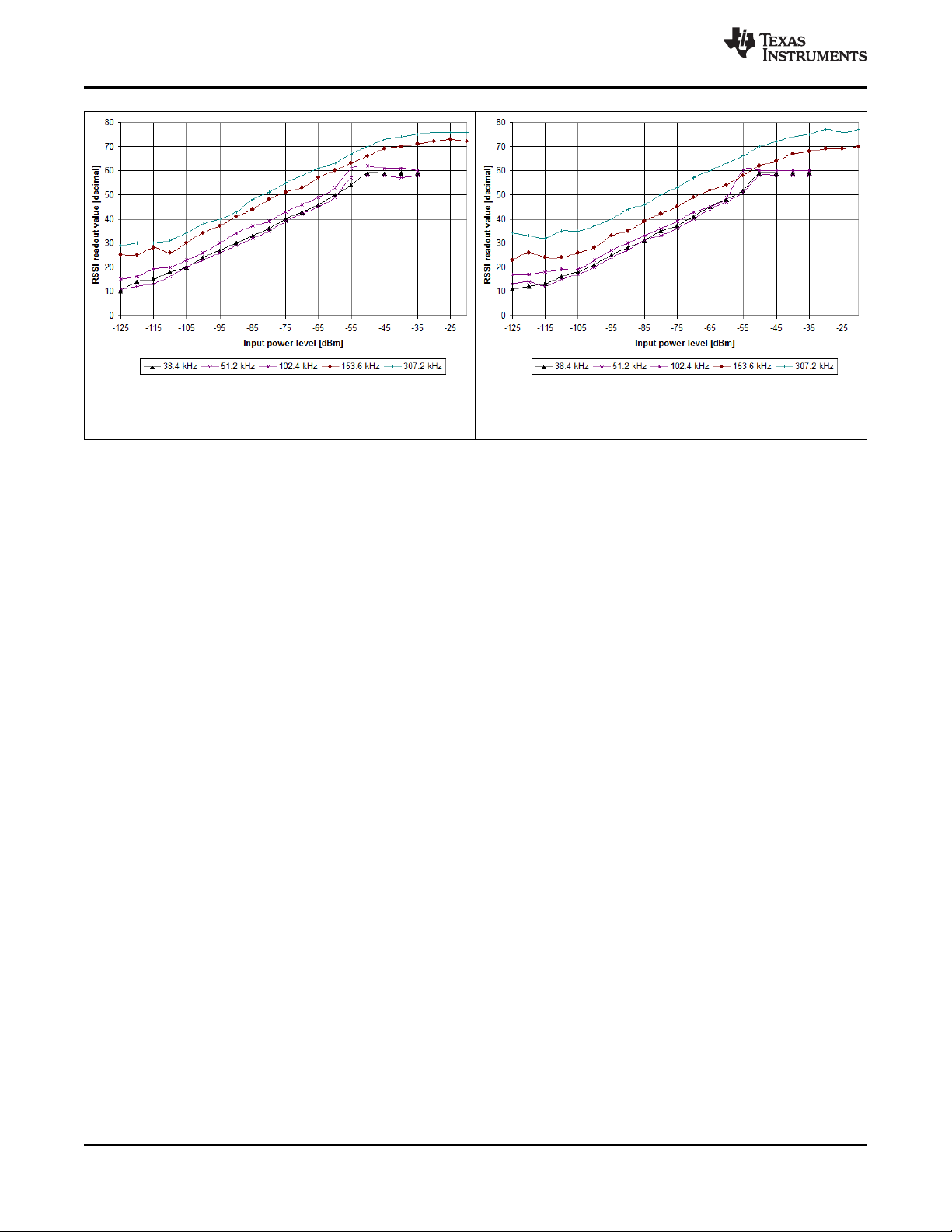
CC1020
SWRS046H –NOVEMBER 2006–REVISED MARCH 2015
www.ti.com
Figure 5-11. Typical RSSI Value vs Input Power for Some Figure 5-12. Typical RSSI Value vs Input Power for Some
Typical Channel Spacings, 433 MHz Typical Channel Spacings, 868 MHz
5.9.6 Image Rejection Calibration
For perfect image rejection, the phase and gain of the “I” and “Q” parts of the analog RX chain must be
perfectly matched. To improve the image rejection, the “I” and “Q” phase and gain difference can be finetuned by adjusting the PHASE_COMP and GAIN_COMP registers. This allows compensation for process
variations and other nonidealities. The calibration is done by injecting a signal at the image frequency, and
adjusting the phase and gain difference for minimum RSSI value.
During image rejection calibration, an unmodulated carrier should be applied at the image frequency
(614.4 kHz below the desired channel). No signal should be present in the desired channel. The signal
level should be 50 to 60 dB above the sensitivity in the desired channel, but the optimum level will vary
from application to application. Too large input level gives poor results due to limited linearity in the analog
IF chain, while too low input level gives poor results due to the receiver noise floor.
For best RSSI accuracy, use AGC_AVG[1:0] = 11 during image rejection calibration (RSSI value is
averaged over 16 filter output samples). The RSSI register update rate then equals the receiver channel
bandwidth (set in FILTER register) divided by 8, as the filter output rate is twice the receiver channel
bandwidth. This gives the minimum waiting time between RSSI register reads (0.5 ms is used below). TI
recommends the following image calibration procedure:
1. Define 3 variables: XP = 0, XG = 0 and DX = 64. Go to step 3.
2. Set DX = DX/2.
3. Write XG to GAIN_COMP register.
4. If XP + 2 × DX < 127, then
5. Wait at least 3 ms. Measure signal strength Y4 as filtered average of 8 reads from RSSI register with
6. Write XP+DX to PHASE_COMP register.
7. Wait at least 3 ms. Measure signal strength Y3 as filtered average of 8 reads from RSSI register with
8. Write XP to PHASE_COMP register.
9. Wait at least 3 ms. Measure signal strength Y2 as filtered average of 8 reads from RSSI register with
10. Write XP-DX to PHASE_COMP register.
11. Wait at least 3 ms. Measure signal strength Y1 as filtered average of 8 reads from RSSI register with
32 Detailed Description Copyright © 2006–2015, Texas Instruments Incorporated
write XP + 2 × DX to PHASE_COMP register
else
write 127 to PHASE_COMP register.
0.5 ms of delay between each RSSI read.
0.5 ms of delay between each RSSI read.
0.5 ms of delay between each RSSI read.
Submit Documentation Feedback
Product Folder Links: CC1020
Page 33

www.ti.com
12. Write XP – 2 × DX to PHASE_COMP register.
13. Wait at least 3 ms. Measure signal strength Y0 as filtered average of 8 reads from RSSI register with
14. Set AP = 2 × (Y0 – Y2 + Y4) – (Y1 + Y3).
15. If AP > 0 then
16. If DP > DX then
17. Set XP = XP + DP.
18. Write XP to PHASE_COMP register.
19. If XG + 2 × DX < 127 then
20. Wait at least 3 ms. Measure signal strength Y4 as filtered average of 8 reads from RSSI register with
21. Write XG + DX to GAIN_COMP register.
22. Wait at least 3 ms. Measure signal strength Y3 as filtered average of 8 reads from RSSI register with
23. Write XG to GAIN_COMP register.
24. Wait at least 3 ms. Measure signal strength Y2 as filtered average of 8 reads from RSSI register with
25. Write XG – DX to GAIN_COMP register.
26. Wait at least 3 ms. Measure signal strength Y1 as filtered average of 8 reads from RSSI register with
27. Write XG – 2 × DX to GAIN_COMP register.
28. Wait at least 3 ms. Measure signal strength Y0 as filtered average of 8 reads from RSSI register with
29. Set AG = 2 × (Y0 – Y2 + Y4) – (Y1 + Y3).
30. If AG > 0 then
31. If DG > DX then
32. Set XG = XG + DG.
33. If DX > 1 then go to step 2.
34. Write XP to PHASE_COMP register and XG to GAIN_COMP register.
CC1020
SWRS046H –NOVEMBER 2006–REVISED MARCH 2015
0.5 ms of delay between each RSSI read.
0.5 ms of delay between each RSSI read.
set DP = ROUND ( 7 × DX × (2 × (Y0 – Y4) + Y1 – Y3) / (10 × AP))
else
if Y0 + Y1 > Y3 + Y4 then
set DP = DX
else
set DP = –DX.
set DP = DX
else
if DP < –DX then set DP = –DX.
write XG + 2 × DX to GAIN_COMP register
else
write 127 to GAIN_COMP register.
0.5 ms of delay between each RSSI read.
0.5 ms of delay between each RSSI read.
0.5 ms of delay between each RSSI read.
0.5 ms of delay between each RSSI read.
0.5 ms of delay between each RSSI read.
set DG = ROUND (7 × DX × (2 × (Y0 – Y4) + Y1 – Y3) / (10 × AG)
else
if Y0 + Y1 > Y3 + Y4 then
set DG = DX
else
set DG = –DX.
set DG = DX
else
if DG < –DX then set DG = –DX
If repeated calibration gives varying results, try to change the input level or increase the number of RSSI
reads N. A good starting point is N = 8. As accuracy is more important in the last fine-calibration steps, it
can be worthwhile to increase N for each loop iteration.
Copyright © 2006–2015, Texas Instruments Incorporated Detailed Description 33
Submit Documentation Feedback
Product Folder Links: CC1020
Page 34

CC1020
SWRS046H –NOVEMBER 2006–REVISED MARCH 2015
For high frequency deviation and high data rates (typically ≥ 76.8 kBaud) the analog filter succeeding the
mixer must be bypassed by setting FILTER_BYPASS = 1 in the FILTER register. In this case the image
rejection is degraded.
The image rejection is reduced for low supply voltages (typically < 2.5 V) when operating in the 402 to 470
MHz frequency range.
5.9.7 Blocking and Selectivity
Figure 5-13 shows the blocking/selectivity at 433 MHz, 12.5 kHz channel spacing. Figure 5-14 shows the
blocking/selectivity at 868 MHz, 25 kHz channel spacing. The blocking rejection is the ratio between a
modulated blocker (interferer) and a wanted signal 3 dB above the sensitivity limit.
www.ti.com
Figure 5-13. Typical Blocker Rejection
(12.5 kHz Channel Spacing, 12.288 kHz Receiver Channel Filter
Carrier Frequency Set to 434.3072 MHz
Bandwidth)
5.9.8 Linear IF Chain and AGC Settings
CC1020 is based on a linear IF chain where the signal amplification is done in an analog VGA (Variable
Gain Amplifier). The gain is controlled by the digital part of the IF chain after the ADC (Analog to Digital
Converter). The AGC (Automatic Gain Control) loop ensures that the ADC operates inside its dynamic
range by using an analog/digital feedback loop.
The maximum VGA gain is programmed by the VGA_SETTING[4:0] in the VGA3 register. The VGA gain
is programmed in approximately 3 dB/LSB. The VGA gain should be set so that the amplified thermal
noise from the front-end balance the quantization noise from the ADC. Therefore the optimum maximum
VGA gain setting will depend on the channel filter bandwidth.
A digital RSSI is used to measure the signal strength after the ADC. The CS_LEVEL[4:0] in the VGA4
register is used to set the nominal operating point of the gain control (and also the carrier sense level).
Further explanation can be found in Figure 5-15.
The VGA gain will be changed according to a threshold set by the VGA_DOWN[2:0] in the VGA3 register
and the VGA_UP[2:0] in the VGA4 register. Together, these two values specify the signal strength limits
used by the AGC to adjust the VGA gain.
To avoid unnecessary tripping of the VGA, an extra hysteresis and filtering of the RSSI samples can be
added. The AGC_HYSTERESIS bit in the VGA2 register enables this.
Figure 5-14. Typical Blocker Rejection
(25 kHz Channel Spacing, 19.2 kHz Receiver Channel Filter
Carrier Frequency Set to 868.3072 MHz
Bandwidth)
The time dynamics of the loop can be altered by the VGA_BLANKING bit in the ANALOG register, and
VGA_FREEZE[1:0] and VGA_WAIT[2:0] bits in the VGA1 register.
When VGA_BLANKING is activated, the VGA recovery time from DC offset spikes after a gain step is
reduced.
34 Detailed Description Copyright © 2006–2015, Texas Instruments Incorporated
Submit Documentation Feedback
Product Folder Links: CC1020
Page 35

RSSI Level
0
Zero level depends on front-end settings and VGA_SETTING
value.
CS_LEVEL+8
VGA_UP
VGA_DOWN+3
(signal strength, 1.5dB/step)
Carrier sense is turned on here.
AGC increases gain if below this
level (unless at maximum).
AGC decreases gain if above
this level (unless at minimum).
To set CS_LEVEL, subtract 8 from RSSI readout with RF
input signal at desired carrier sense level.
Note that the AGC works with "raw" filter output signal
strength, while the RSSI readout value is compensated for
VGA gain changes by the AGC.
The AGC keeps the signal strength in this range. Minimize
VGA_DOWN for best selectivity, but leave some margin to
avoid frequent VGA gain changes during reception.
The AGC keeps the signal strength above carrier sense level
+ VGA_UP. Minimize VGA_UP for best selectivity, but
increase if first VGA gain reduction occurs too close to the
noise floor.
www.ti.com
VGA_FREEZE determines the time to hold bit synchronization, VGA and RSSI levels after one of these
events occur:
• RX power-up
• The PLL has been out of lock
• Frequency register setting is switched between A and B
This feature is useful to avoid AGC operation during start-up transients and to ensure minimum dwell time
using frequency hopping. This means that bit synchronization can be maintained from hop to hop.
VGA_WAIT determines the time to hold the present bit synchronization and RSSI levels after changing
VGA gain. This feature is useful to avoid AGC operation during the settling of transients after a VGA gain
change. Some transients are expected due to DC offsets in the VGA.
At the sensitivity limit, the VGA gain is set by VGA_SETTING. In order to optimize selectivity, this gain
should not be set higher than necessary. The SmartRF Studio software gives the settings for VGA1 to
VGA4 registers. For reference, the following method can be used to find the AGC settings:
1. Disable AGC and use maximum LNA2 gain by writing BFh to the VGA2 register. Set minimum VGA
2. Apply no RF input signal, and measure ADC noise floor by reading the RSSI register.
3. Apply no RF input signal, and write VGA3 register with increasing VGA_SETTING value until the RSSI
4. Apply an RF signal with strength equal the desired carrier sense threshold. The RF signal should
5. If desired, adjust the VGA_UP and VGA_DOWN settings according to the explanation in Figure 5-15.
6. Enable AGC and select LNA2 gain change level. Write 55h to VGA2 register if the resulting
CC1020
SWRS046H –NOVEMBER 2006–REVISED MARCH 2015
gain by writing to the VGA3 register with VGA_SETTING = 0.
register value is approximately 4 larger than the value read in step 2. This places the front-end noise
floor around 6 dB above the ADC noise floor.
preferably be modulated with correct Baud rate and deviation. Read the RSSI register value, subtract
8, and write to CS_LEVEL in the VGA4 register. Vary the RF signal level slightly and check that carrier
sense indication (bit 3 in STATUS register) switches at the desired input level.
VGA_SETTING>10. Otherwise, write 45h to VGA2. Modify AGC_AVG in the above VGA2 value if
faster carrier sense and AGC settling is desired.
Copyright © 2006–2015, Texas Instruments Incorporated Detailed Description 35
Figure 5-15. Relationship Between RSSI, Carrier Sense Level,
and AGC Settings CS_LEVEL, VGA_UP and VGA_DOWN
Submit Documentation Feedback
Product Folder Links: CC1020
Page 36

CC1020
SWRS046H –NOVEMBER 2006–REVISED MARCH 2015
5.9.9 AGC Settling
After turning on the RX chain, the following occurs:
A. The AGC waits 16 to 128 ADC_CLK (1.2288 MHz) periods, depending on the VGA_FREEZE setting in
the VGA1 register, for settling in the analog parts.
B. The AGC waits 16 to 48 FILTER_CLK periods, depending on the VGA_WAIT setting in the VGA1
register, for settling in the analog parts and the digital channel filter.
C. The AGC calculates the RSSI value as the average magnitude over the next 2 to 16 FILTER_CLK
periods, depending on the AGC_AVG setting in the VGA2 register.
D. If the RSSI value is higher than CS_LEVEL+8, then the carrier sense indicator is set (if CS_SET = 0).
If the RSSI value is too high according to the CS_LEVEL, VGA_UP and VGA_DOWN settings, and the
VGA gain is not already at minimum, then the VGA gain is reduced and the AGC continues from B).
E. If the RSSI value is too low according to the CS_LEVEL and VGA_UP settings, and the VGA gain is
not already at maximum (given by VGA_SETTING), then the VGA gain is increased and the AGC
continues from B).
Two to three VGA gain changes should be expected before the AGC has settled. Increasing AGC_AVG
increases the settling time, but may be worthwhile if there is the time in the protocol, and for reducing false
wake-up events when setting the carrier sense close to the noise floor.
The AGC settling time depends on the FILTER_CLK (= 2 × ChBW). Thus, there is a trade off between
AGC settling time and receiver sensitivity because the AGC settling time can be reduced for data rates
lower than 76.8 kBaud by using a wider receiver channel filter bandwidth (that is, larger ChBW).
www.ti.com
5.9.10 Preamble Length and Sync Word
The rules for choosing a good sync word are as follows:
1. The sync word should be significantly different from the preamble.
2. A large number of transitions is good for the bit synchronization or clock recovery. Equal bits reduce
the number of transitions. The recommended sync word has at most 3 equal bits in a row.
3. Autocorrelation. The sync word should not repeat itself, as this will increase the likelihood for errors.
4. In general the first bit of sync should be opposite of last bit in preamble, to achieve one more transition.
The recommended sync words for CC1020 are 2 bytes (0xD391), 3 bytes (0xD391DA) or 4 bytes
(0xD391DA26) and are selected as the best compromise of the above criteria.
Using the register settings provided by the SmartRFM Studio software, packet error rates (PER) less than
0.5% can be achieved when using 24 bits of preamble and a 16 bit sync word (0xD391). Using a
preamble longer than 24 bits will improve the PER.
When performing the PER measurements described above the packet format consisted of 10 bytes of
random data, 2 bytes CRC and 1 dummy byte in addition to the sync word and preamble at the start of
each package.
For the test, 1000 packets were sent 10 times. The transmitter was put in power down between each
packet. Any bit error in the packet, either in the sync word, in the data or in the CRC caused the packet to
be counted as a failed packet.
36 Detailed Description Copyright © 2006–2015, Texas Instruments Incorporated
Submit Documentation Feedback
Product Folder Links: CC1020
Page 37

www.ti.com
5.9.11 Carrier Sense
The carrier sense signal is based on the RSSI value and a programmable threshold. The carrier sense
function can be used to simplify the implementation of a CSMA (Carrier Sense Multiple Access) medium
access protocol.
Carrier sense threshold level is programmed by CS_LEVEL[4:0] in the VGA4 register and
VGA_SETTING[4:0] in the VGA3 register.
VGA_SETTING[4:0] sets the maximum gain in the VGA. This value must be set so that the ADC works
with optimum dynamic range for a certain channel filter bandwidth. The detected signal strength (after the
ADC) will therefore depend on this setting.
CS_LEVEL[4:0] sets the threshold for this specific VGA_SETTING[4:0] value. If the VGA_SETTING[4:0] is
changed, the CS_LEVEL[4:0] must be changed accordingly to maintain the same absolute carrier sense
threshold. See Figure 5-15 for an explanation of the relationship between RSSI, AGC and carrier sense
settings.
The carrier sense signal can be read as the CARRIER_SENSE bit in the STATUS register.
The carrier sense signal can also be made available at the LOCK pin by setting LOCK_SELECT[3:0] =
0100 in the LOCK register.
5.9.12 Automatic Power-up Sequencing
CC1020
SWRS046H –NOVEMBER 2006–REVISED MARCH 2015
CC1020 has a built-in automatic power-up sequencing state machine. By setting the CC1020 into this
mode, the receiver can be powered-up automatically by a wake-up signal and will then check for a carrier
signal (carrier sense). If carrier sense is not detected, it returns to power-down mode. A flow chart for
automatic power-up sequencing is shown in Figure 5-16.
The automatic power-up sequencing mode is selected when PD_MODE[1:0] = 11 in the MAIN register.
When the automatic power-up sequencing mode is selected, the functionality of the MAIN register is
changed and used to control the sequencing.
By setting SEQ_PD = 1 in the MAIN register, CC1020 is set in power down mode. If SEQ_PSEL = 1 in the
SEQUENCING register the automatic power-up sequence is initiated by a negative transition on the PSEL
pin.
If SEQ_PSEL = 0 in the SEQUENCING register, then the automatic power-up sequence is initiated by a
negative transition on the DIO pin (as long as SEP_DI_DO = 1 in the INTERFACE register).
Sequence timing is controlled through RX_WAIT[2:0] AND CS_WAIT[3:0] in the SEQUENCING register.
VCO and PLL calibration can also be done automatically as a part of the sequence. This is controlled
through SEQ_CAL[1:0] in the MAIN register. Calibration can be done every time, every 16th sequence,
every 256th sequence, or never. See Section 5.22.1 description for details. A description of when to do,
and how the VCO and PLL self-calibration is done, is given in Section 5.12.2.
See also Application Note AN070 CC1020 Automatic Power-Up Sequencing (SWRA279).
Copyright © 2006–2015, Texas Instruments Incorporated Detailed Description 37
Submit Documentation Feedback
Product Folder Links: CC1020
Page 38
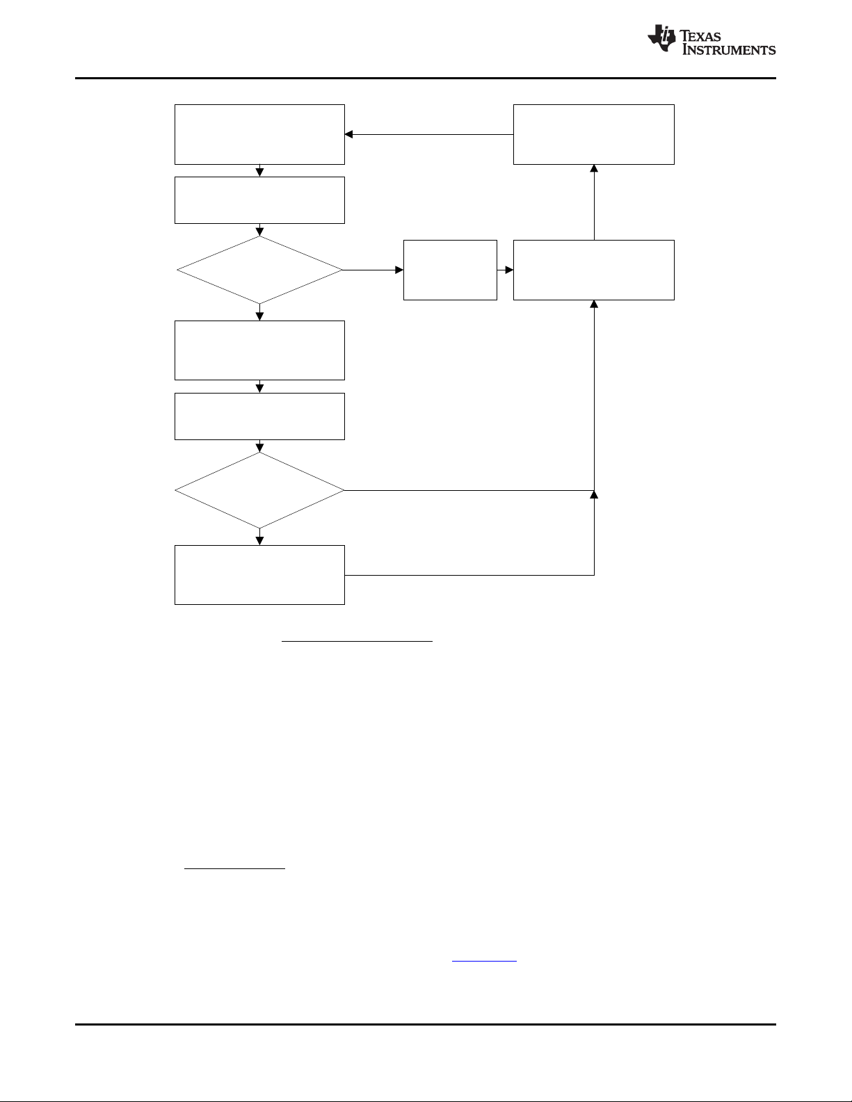
AFC Baud rate
F
16
´
[ ]
xoscx
ADC
f
2 (ADC _ DIV 2 : 0 1)
=
´ +
Power down
Crystal oscillator and bias off
Frequency synthesizer off
Receive chain off
Wait for PLL
lock or timeout,
127 filter clocks
Turn on crystal oscillator/bias
Frequency synthesizer off
Receive chain off
Crystal oscillator and bias on
Turn on frequency synthesizer
Receive chain off
Optional waiting time before
turning on receive chain
Programmable:
32-256 ADC clocks
Crystal oscillator and bias on
Frequency synthesizer on
Turn on receive chain
Receive mode
Crystal oscillator and bias on
Frequency synthesizer on
Receive chain on
Wait for
carrier sense or timeout
Programmable: 20-72
filter clocks
Set
SEQ_ERROR
flag in STATUS
register
Optional calibration
Programmable: each time,
once in 16, or once in 256
Receive chain off
PLL in lock
PLL timeout
Sequencing wake-up event
Carrier sense timeout
Carrier sense
(negative transition on
PSEL pin or DIO pin)
(Positive transition on SEQ_PD in MAIN register)
Sequencing power-down event
CC1020
SWRS046H –NOVEMBER 2006–REVISED MARCH 2015
www.ti.com
(1) Filter clock (FILTER_CLK): f
(2) ADC clock (ADC_CLK): where ADC_DIV[2:0] is set in the MODEM register.
5.9.13 Automatic Frequency Control
CC1020 has a built-in feature called AFC (Automatic Frequency Control) that can be used to compensate
for frequency drift.
The average frequency offset of the received signal (from the nominal IF frequency) can be read in the
AFC register. The signed (2’s-complement) 8-bit value AFC[7:0] can be used to compensate for frequency
offset between transmitter and receiver.
The frequency offset is given by Equation 22.
The receiver can be calibrated against the transmitter by changing the operating frequency according to
the measured offset. The new frequency must be calculated and written to the FREQ register by the
microcontroller. The AFC can be used for an FSK/GFSK signal, but not for OOK. Application Note AN029
CC1020/1021 Automatic Frequency Control (AFC) (SWRA063) provides the procedure and equations
necessary to implement AFC.
The AFC feature reduces the crystal accuracy requirement.
filter_clock
Figure 5-16. Automatic Power-up Sequencing Flow Chart
= 2 × ChBW where ChBW is defined in Section 5.9.2.
(22)
38 Detailed Description Copyright © 2006–2015, Texas Instruments Incorporated
Submit Documentation Feedback
Product Folder Links: CC1020
Page 39

GAUSS _ FILTER Baud rate
8
´
=
www.ti.com
5.9.14 Digital FM
It is possible to read back the instantaneous IF from the FM demodulator as a frequency offset from the
nominal IF frequency. This digital value can be used to perform a pseudo analog FM demodulation.
The frequency offset can be read from the GAUSS_FILTER register and is a signed 8-bit value coded as
2-complement.
The instantaneous deviation is given by Equation 23.
The digital value should be read from the register and sent to a DAC and filtered in order to get an analog
audio signal. The internal register value is updated at the MODEM_CLK rate. MODEM_CLK is available at
the LOCK pin when LOCK_SELECT[3:0] = 1101 in the LOCK register, and can be used to synchronize
the reading.
For audio (300 to 4000 Hz) the sampling rate should be higher than or equal to 8 kHz (Nyquist) and is
determined by the MODEM_CLK. The MODEM_CLK, which is the sampling rate, equals 8 times the baud
rate. That is, the minimum baud rate, which can be programmed, is 1 kBaud. However, the incoming data
will be filtered in the digital domain and the 3-dB cut-off frequency is 0.6 times the programmed Baud rate.
Thus, for audio the minimum programmed Baud rate should be approximately 7.2 kBaud.
The GAUSS_FILTER resolution decreases with increasing baud rate. A accumulate and dump filter can
be implemented in the µC to improve the resolution. Note that each GAUSS_FILTER reading should be
synchronized to the MODEM_CLK. As an example, accumulating 4 readings and dividing the total by 4
will improve the resolution by 2 bits.
CC1020
SWRS046H –NOVEMBER 2006–REVISED MARCH 2015
(23)
Furthermore, to fully utilize the GAUSS_FILTER dynamic range the frequency deviation must be 16 times
the programmed baud rate.
5.10 Transmitter
5.10.1 FSK Modulation Formats
The data modulator can modulate FSK, which is a two level FSK (Frequency Shift Keying), or GFSK,
which is a Gaussian filtered FSK with BT = 0.5. The purpose of the GFSK is to make a more bandwidth
efficient system as shown in Figure 5-17. The modulation and the Gaussian filtering are done internally in
the chip. The TX_SHAPING bit in the DEVIATION register enables the GFSK. GFSK is recommended for
narrowband operation.
Figure 5-18 and Figure 5-19 show typical eye diagrams for 434 MHz and 868 MHz operation, respectively.
Copyright © 2006–2015, Texas Instruments Incorporated Detailed Description 39
Submit Documentation Feedback
Product Folder Links: CC1020
Page 40
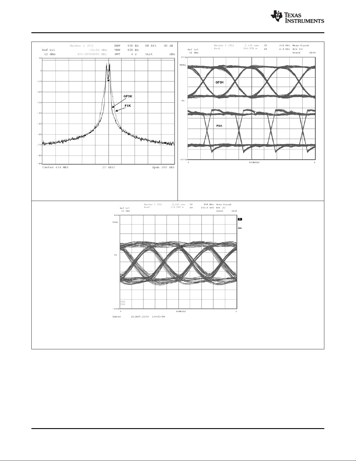
CC1020
SWRS046H –NOVEMBER 2006–REVISED MARCH 2015
www.ti.com
2.4 kBaud, NRZ, ±2.025 kHz
frequency deviation
Figure 5-17. FSK vs GFSK Spectrum Plot
153.6 kBaud, NRZ, ±79.2 kHz frequency
Figure 5-19. GFSK Eye Diagram
2.4 kBaud, NRZ, ±2.025 kHz
frequency deviation
Figure 5-18. FSK vs GFSK Eye Diagram
deviation
5.10.2 Output Power Programming
The RF output power from the device is programmable by the 8-bit PA_POWER register. Figure 5-20 and
Figure 5-21 show the output power and total current consumption as a function of the PA_POWER
register setting. It is more efficient in terms of current consumption to use either the lower or upper 4-bits
in the register to control the power, as shown in Figure 5-20 and Figure 5-21. However, the output power
can be controlled in finer steps using all the available bits in the PA_POWER register.
40 Detailed Description Copyright © 2006–2015, Texas Instruments Incorporated
Submit Documentation Feedback
Product Folder Links: CC1020
Page 41
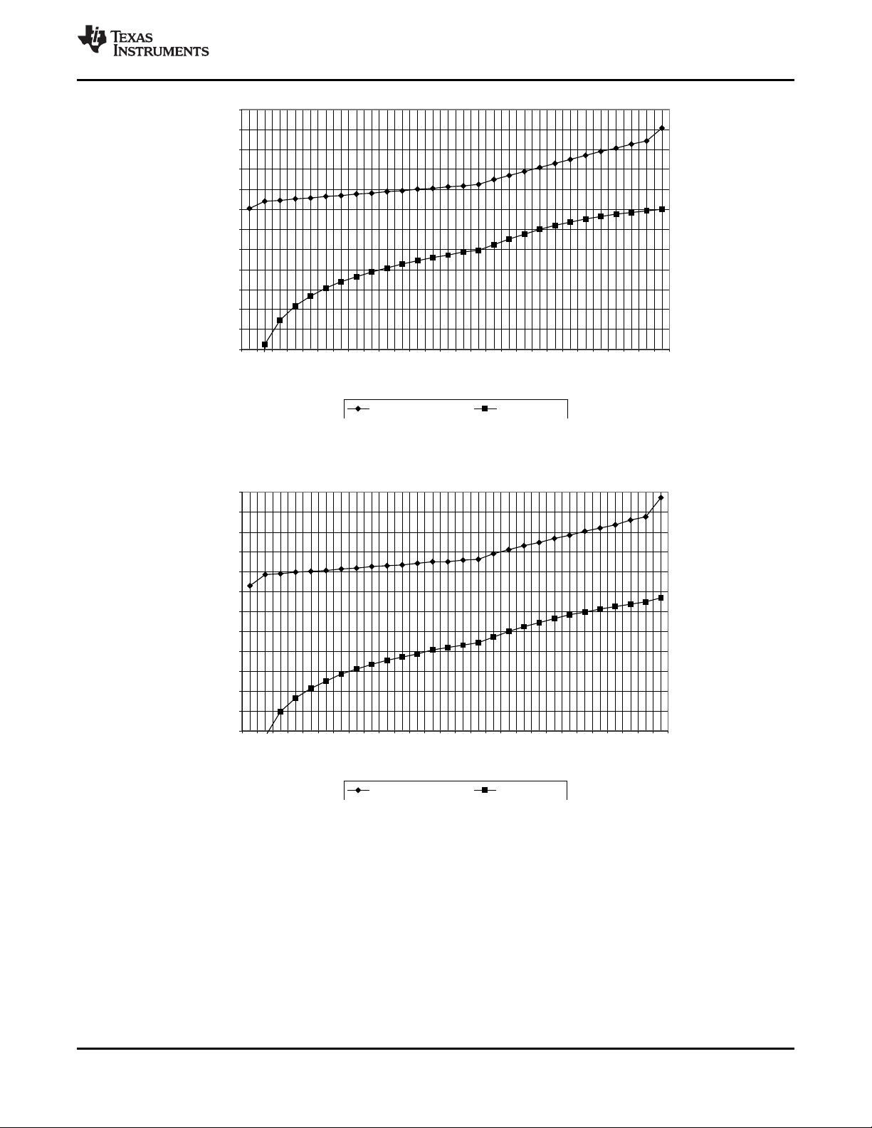
-25.0
-20.0
-15.0
-10.0
-5.0
0.0
5.0
10.0
15.0
20.0
25.0
30.0
35.0
0 1 2 3 4 5 6 7 8 9 0A 0B 0C 0D 0E 0F 50 60 70 80 90 A0 B0 C0 D0 E0 F0 FF
PA_POWER [hex ]
Current [mA] / Output power [dBm]
Current Consumption Output Power
-25.0
-20.0
-15.0
-10.0
-5.0
0.0
5.0
10.0
15.0
20.0
25.0
30.0
35.0
0 1 2 3 4 5 6 7 8 9 0A 0B 0C 0D 0E 0F 50 60 70 80 90 A0 B0 C0 D0 E0 F0 FF
PA_POWER [hex ]
Current [mA] / Output power [dBm]
Current Consumption Output Power
www.ti.com
CC1020
SWRS046H –NOVEMBER 2006–REVISED MARCH 2015
Figure 5-20. Typical Output Power and Current Consumption, 433 MHz
5.10.3 TX Data Latency
The transmitter will add a delay due to the synchronization of the data with DCLK and further clocking into
the modulator. The user should therefore add a delay equivalent to at least 2 bits after the data payload
has been transmitted before switching off the PA (that is, before stopping the transmission).
Copyright © 2006–2015, Texas Instruments Incorporated Detailed Description 41
Figure 5-21. Typical Output Power and Current Consumption, 433 MHz
Submit Documentation Feedback
Product Folder Links: CC1020
Page 42

CC1021
RF_OUT
RF_IN
C60
R10
L2
C3
L1
C1
C71 C72
L70 L71
T/R
SWITCH
AVDD = 3 V
ANTENNA
CC1020
SWRS046H –NOVEMBER 2006–REVISED MARCH 2015
5.10.4 Reducing Spurious Emission and Modulation Bandwidth
Modulation bandwidth and spurious emission are normally measured with the PA continuously on and a
repeated test sequence.
In cases where the modulation bandwidth and spurious emission are measured with the CC1020
switching from power down mode to TX mode, a PA ramping sequence could be used to minimize
modulation bandwidth and spurious emission.
PA ramping should then be used both when switching the PA on and off. A linear PA ramping sequence
can be used where register PA_POWER is changed from 00h to 0Fh and then from 50h to the register
setting that gives the desired output power (for example, F0h for +10 dBm output power at 433 MHz
operation). The longer the time per PA ramping step the better, but setting the total PA ramping time equal
to 2 bit periods is a good compromise between performance and PA ramping time.
5.11 Input and Output Matching and Filtering
When designing the impedance matching network for the CC1020 the circuit must be matched correctly at
the harmonic frequencies as well as at the fundamental tone. A recommended matching network is shown
in Figure 5-22. Component values for various frequencies are given in Table 5-8. Component values for
other frequencies can be found using the SmartRF Studio software.
As can be seen from Figure 5-22 and Table 5-8, the 433 MHz network utilizes a T-type filter, while the
868/915 MHz network has a π-type filter topology.
www.ti.com
It is important to remember that the physical layout and the components used contribute significantly to
the reflection coefficient, especially at the higher harmonics. For this reason, the frequency response of
the matching network should be measured and compared to the response of the TI reference design.
Refer to Figure 5-24 and Table 5-9 as well as Figure 5-25 and Table 5-10.
The use of an external T/R switch reduces current consumption in TX for high output power levels and
improves the sensitivity in RX. A recommended application circuit is available from the TI web site
(CC1020EMX). The external T/R switch can be omitted in certain applications, but performance will then
be degraded.
The match can also be tuned by a shunt capacitor array at the PA output (RF_OUT). The capacitance can
be set in 0.4-pF steps and used either in RX mode or TX mode. The RX_MATCH[3:0] and
TX_MATCH[3:0] bits in the MATCH register control the capacitor array.
42 Detailed Description Copyright © 2006–2015, Texas Instruments Incorporated
Figure 5-22. Input and Output Matching Network
Submit Documentation Feedback
Product Folder Links: CC1020
Page 43
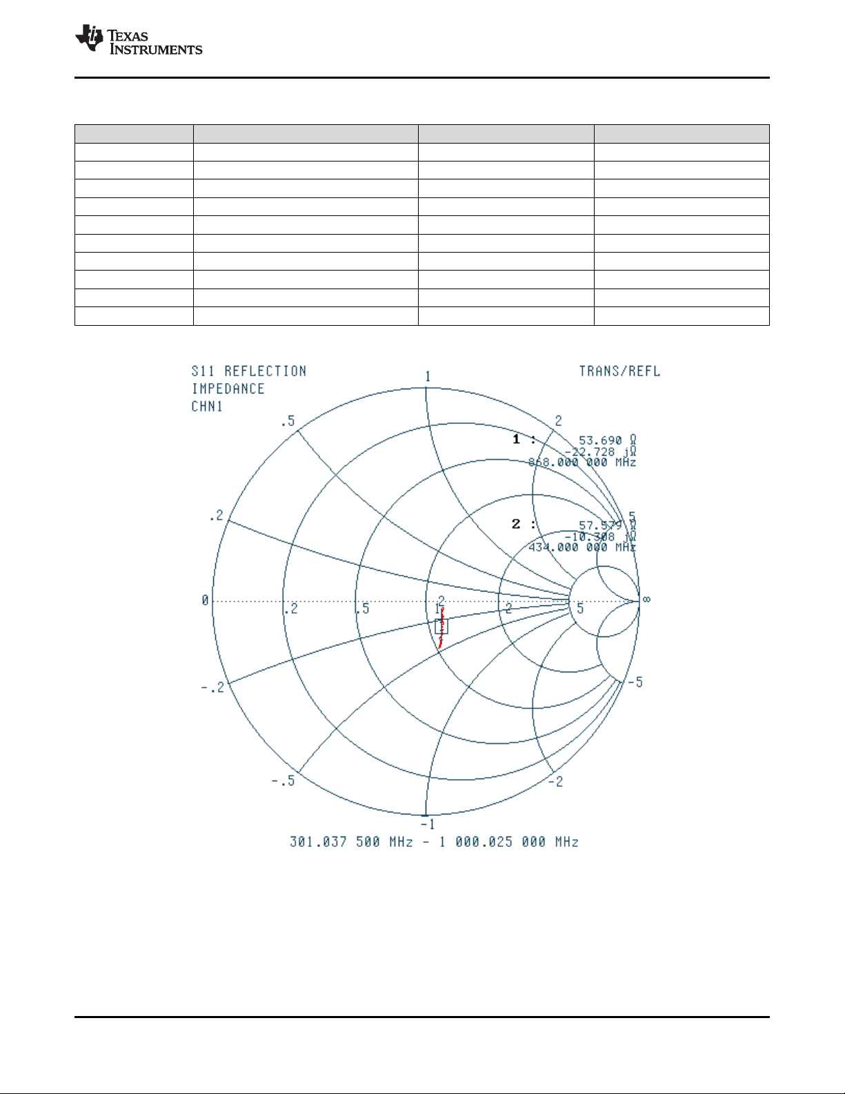
www.ti.com
Table 5-8. Component Values for the Matching Network Described in Figure 5-22
ITEM 433 MHz 868 MHz 915 MHz
C1 10 pF, 5%, NP0, 0402 47 pF, 5%, NP0, 0402 47 pF, 5%, NP0, 0402
C3 5.6 pF, 5%, NP0, 0402 10 pF, 5%, NP0, 0402 10 pF, 5%, NP0, 0402
C60 220 pF, 5%, NP0, 0402 220 pF, 5%, NP0, 0402 220 pF, 5%, NP0, 0402
C71 DNM
C72 4.7 pF, 5%, NP0, 0402 8.2 pF 5%, NP0, 0402 8.2 pF 5%, NP0, 0402
L1 33 nH, 5%, 0402 82 nH, 5%, 0402 82 nH, 5%, 0402
L2 22 nH, 5%, 0402 3.6 nH, 5%, 0402 3.6 nH, 5%, 0402
L70 47 nH, 5%, 0402 5.1 nH, 5%, 0402 5.1 nH, 5%, 0402
L71 39 nH, 5%, 0402 0 Ω resistor, 0402 0 Ω resistor, 0402
R10 82 Ω, 5%, 0402 82 Ω, 5%, 0402 82 Ω, 5%, 0402
(1) DNM = Do Not Mount
CC1020
SWRS046H –NOVEMBER 2006–REVISED MARCH 2015
(1)
8.2 pF 5%, NP0, 0402 8.2 pF 5%, NP0, 0402
Figure 5-23. Typical LNA Input Impedance, 200 to 1000 MHz
Copyright © 2006–2015, Texas Instruments Incorporated Detailed Description 43
Submit Documentation Feedback
Product Folder Links: CC1020
Page 44
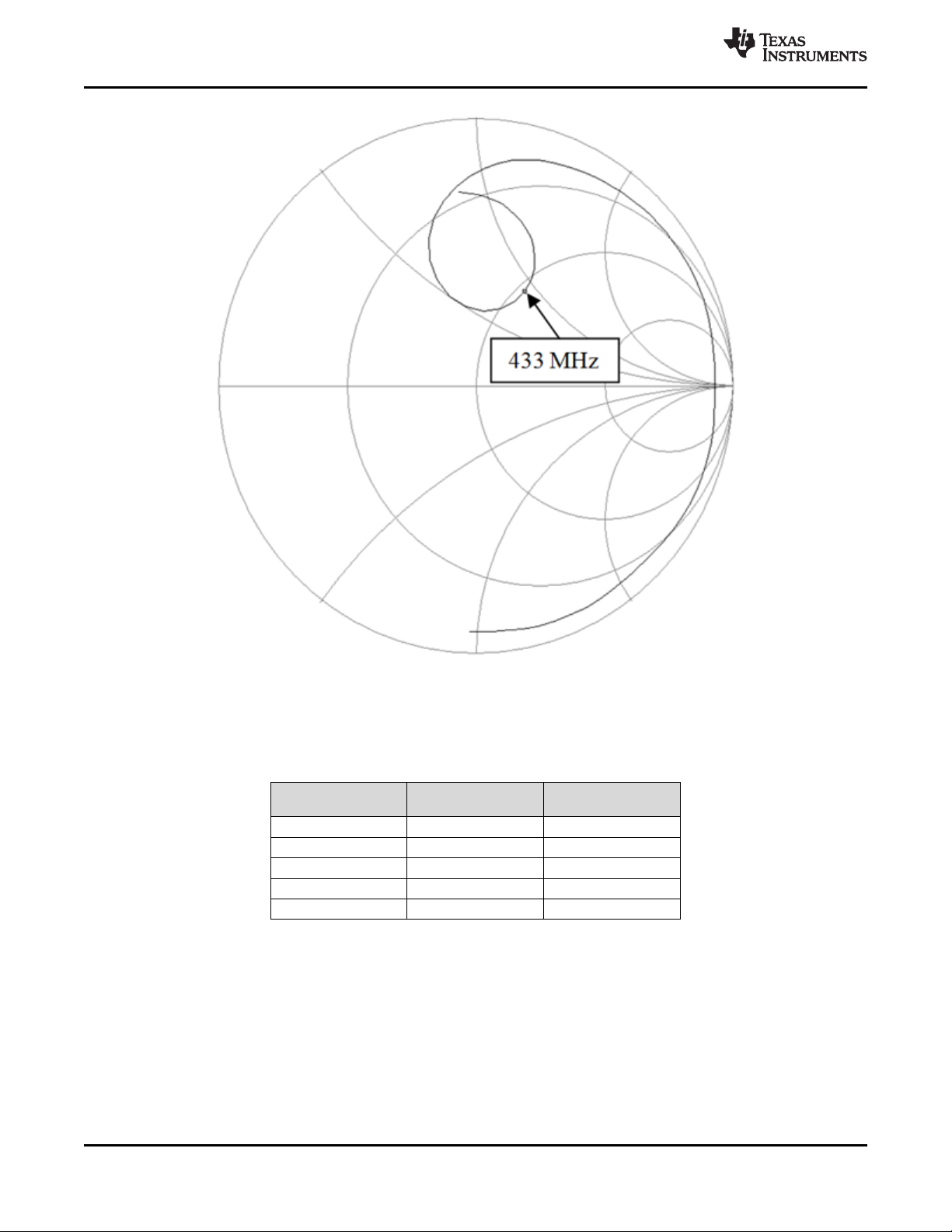
CC1020
SWRS046H –NOVEMBER 2006–REVISED MARCH 2015
www.ti.com
The frequency is swept from 300 MHz to 2500 MHz. Values are listed in .
Figure 5-24. Typical Optimum PA Load Impedance, 433 MHz
Table 5-9. Impedances at the First 5 Harmonics
(433 MHz Matching Network)
FREQUENCY REAL IMAGINARY
(MHz) (Ohms) (Ohms)
433 54 44
866 20 173
1299 288 –563
1732 14 –123
2165 5 –66
44 Detailed Description Copyright © 2006–2015, Texas Instruments Incorporated
Submit Documentation Feedback
Product Folder Links: CC1020
Page 45
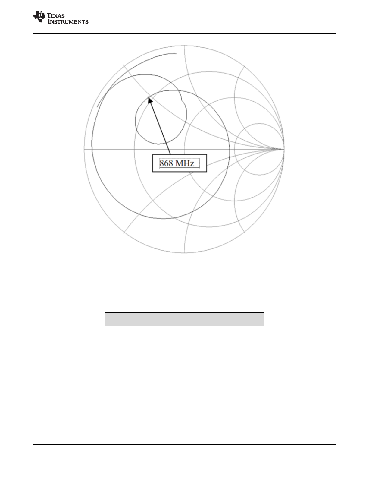
www.ti.com
CC1020
SWRS046H –NOVEMBER 2006–REVISED MARCH 2015
The frequency is swept from 300 MHz to 2800 MHz. Values are listed in Table 5-10.
Figure 5-25. Typical optimum PA load impedance, 868/915 MHz
Table 5-10. Impedances at the First Three Harmonics
(868/915 MHz Matching Network)
FREQUENCY REAL IMAGINARY
(MHz) (Ohms) (Ohms)
868 15 24
915 20 35
1736 1.5 18
1830 1.7 22
2604 3.2 44
2745 3.6 45
5.12 Frequency Synthesizer
5.12.1 VCO, Charge Pump and PLL Loop Filter
The VCO is completely integrated and operates in the 1608 to 1920 MHz range. A frequency divider is
used to get a frequency in the UHF range (402 to 470 and 804 to 960 MHz). The BANDSELECT bit in the
ANALOG register selects the frequency band.
Copyright © 2006–2015, Texas Instruments Incorporated Detailed Description 45
Submit Documentation Feedback
Product Folder Links: CC1020
Page 46

ref
min
f
220
= ´
[ ]
ref
2
f
BW
æ ö
= -
ç ÷
è ø
[ ]
ref
BW
f
æ ö
= W
ç ÷
è ø
[ ]
ref
2
f
BW
æ ö
=
ç ÷
è ø
[ ]
ref
BW
f
æ ö
= W
ç ÷
è ø
[ ]
ref
2
f
BW
æ ö
= -
ç ÷
è ø
VCO ref
FREQ 0.5 DITHER
8192
+ ´
æ ö
= ´ +
ç ÷
è ø
CC1020
SWRS046H –NOVEMBER 2006–REVISED MARCH 2015
The VCO frequency is given by Equation 24.
The VCO frequency is divided by 2 and by 4 to generate frequencies in the two bands, respectively.
The VCO sensitivity (sometimes referred to as VCO gain) varies over frequency and operating conditions.
Typically the VCO sensitivity varies between 12 and 36 MHz/V. For calculations the geometrical mean at
21 MHz/V can be used. The PLL calibration (explained below) measures the actual VCO sensitivity and
adjusts the charge pump current accordingly to achieve correct PLL loop gain and bandwidth (higher
charge pump current when VCO sensitivity is lower).
Equation 25 through Equation 29 can be used for calculating PLL loop filter component values, see
Figure 6-1, for a desired PLL loop bandwidth, BW.
www.ti.com
(24)
(25)
(26)
(27)
Define a minimum PLL loop bandwidth as shown in Equation 30.
If BW
> Baud rate/3 then set BW = BW
min
and if BW
min
< Baud rate/3 then set BW = Baud rate/3 in
min
Equation 25 through Equation 29.
There are two special cases when using the recommended 14.7456 MHz crystal:
1. If the data rate is 4.8 kBaud or below and the channel spacing is 12.5 kHz the following loop filter
components are recommended:
C6 = 220 nF
C7 = 8200 pF
C8 = 2200 pF
R2 = 1.5 kΩ
R3 = 4.7 kΩ
2. If the data rate is 4.8 kBaud or below and the channel spacing is different from 12.5 kHz the following
loop filter components are recommended:
C6 = 100 nF
C7 = 3900 pF
C8 = 1000 pF
R2 = 2.2 kΩ
R3 = 6.8 kΩ
(28)
(29)
(30)
46 Detailed Description Copyright © 2006–2015, Texas Instruments Incorporated
Submit Documentation Feedback
Product Folder Links: CC1020
Page 47

[ ]
CHP _ CURRENT / 4
CHP
ref
2
f
7.126
æ ö
= +
ç ÷
è ø
www.ti.com
After calibration the PLL bandwidth is set by the PLL_BW register in combination with the external loop
filter components calculated above. The PLL_BW can be found from Equation 31.
Where:
f
is the reference frequency (in MHz).
ref
The PLL loop filter bandwidth increases with increasing PLL_BW setting. Note that in SmartRF Studio
PLL_BW is fixed to 9E hex when the channel spacing is set up for 12.5 kHz, optimized selectivity.
After calibration the applied charge pump current (CHP_CURRENT[3:0]) can be read in the STATUS1
register. The charge pump current is approximately given by Equation 32.
The combined charge pump and phase detector gain (in A/rad) is given by the charge pump current
divided by 2π.
The PLL bandwidth will limit the maximum modulation frequency and hence, data rate.
5.12.2 VCO and PLL Self-Calibration
To compensate for supply voltage, temperature and process variations, the VCO and PLL must be
calibrated. The calibration is performed automatically and sets the maximum VCO tuning range and
optimum charge pump current for PLL stability. After setting up the device at the operating frequency, the
self-calibration can be initiated by setting the CAL_START bit in the CALIBRATE register. The calibration
result is stored internally in the chip, and is valid as long as power is not turned off. If large supply voltage
drops (typically more than 0.25 V) or temperature variations (typically more than 40°C) occur after
calibration, a new calibration should be performed.
CC1020
SWRS046H –NOVEMBER 2006–REVISED MARCH 2015
(31)
(32)
The nominal VCO control voltage is set by the CAL_ITERATE[2:0] bits in the CALIBRATE register.
The CAL_COMPLETE bit in the STATUS register indicates that calibration has finished. The calibration
wait time (CAL_WAIT) is programmable and is inverse proportional to the internal PLL reference
frequency. The highest possible reference frequency should be used to get the minimum calibration time.
It is recommended to use CAL_WAIT[1:0] = 11 in order to get the most accurate loop bandwidth.
Table 5-11. Typical Calibration Times
CALIBRATION
TIME [ms]
CAL_WAIT 1.8432 7.3728 9.8304
00 49 ms 12 ms 10 ms
01 60 ms 15 ms 11 ms
10 71 ms 18 ms 13 ms
11 109 ms 27 ms 20 ms
REFERENCE FREQUENCY [MHz]
The CAL_COMPLETE bit can also be monitored at the LOCK pin, configured by LOCK_SELECT[3:0] =
0101, and used as an interrupt input to the microcontroller.
To check that the PLL is in lock the user should monitor the LOCK_CONTINUOUS bit in the STATUS
register. The LOCK_CONTINUOUS bit can also be monitored at the LOCK pin, configured by
LOCK_SELECT[3:0] = 0010.
Copyright © 2006–2015, Texas Instruments Incorporated Detailed Description 47
Submit Documentation Feedback
Product Folder Links: CC1020
Page 48

CC1020
SWRS046H –NOVEMBER 2006–REVISED MARCH 2015
There are separate calibration values for the two frequency registers. However, dual calibration is possible
if all of the below conditions apply:
• The two frequencies A and B differ by less than 1 MHz.
• Reference frequencies are equal (REF_DIV_A[2:0] = REF_DIV_B[2:0] in the CLOCK_A/CLOCK_B
registers).
• VCO currents are equal (VCO_CURRENT_A[3:0] = VCO_CURRENT_B[3:0] in the VCO register).
The CAL_DUAL bit in the CALIBRATE register controls dual or separate calibration.
The single calibration algorithm (CAL_DUAL=0) using separate calibration for RX and TX frequency is
illustrated in Figure 5-26. The same algorithm is applicable for dual calibration if CAL_DUAL=1. Refer to
Application Note AN023 CC1020 MCU Interfacing (SWRA069), which includes example source code for
single calibration.
TI recommends that single calibration be used for more robust operation.
There is a small, but finite, possibility that the PLL self-calibration will fail. The calibration routine in the
source code should include a loop so that the PLL is re-calibrated until PLL lock is achieved if the PLL
does not lock the first time. Refer to CC1020 Errata Note 004, available in the CC1020 product folder.
www.ti.com
48 Detailed Description Copyright © 2006–2015, Texas Instruments Incorporated
Submit Documentation Feedback
Product Folder Links: CC1020
Page 49
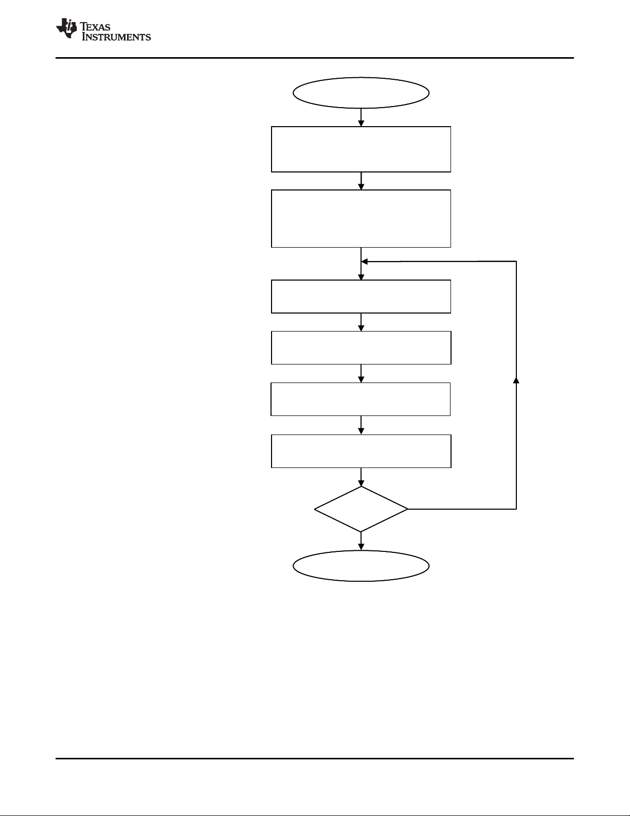
End of calibration
Wait for T≥100 us
Calibrate RX frequency register A
Write MAIN register = 11h:
RXTX=0, F_REG=0, PD_MODE=1,
FS_PD=0, CORE_PD=0, BIAS_PD=0,
RESET_N=1
Write FREQ_A, FREQ_B, VCO,
CLOCK_A and CLOCK_B registers.
PLL_BW = 174 + 16log
2(fref
/7.126)
Start single calibration
Write CALIBRATE register = B4h
ref
is the reference frequency (in
Yes
Read STATUS register and wait until
LOCK_CONTINUOUS=1
Read STATUS register and wait until
CAL_COMPLETE=1
Calibration OK?
No
End of calibrationEnd of calibration
Wait for T≥100 us
Calibrate RX frequency register A
Write MAIN register = 11h:
RXTX=0, F_REG=0, PD_MODE=1,
FS_PD=0, CORE_PD=0, BIAS_PD=0,
RESET_N=1
Write FREQ_A, FREQ_B, VCO,
CLOCK_A and CLOCK_B registers.
PLL_BW = 174 + 16log
2(fref
/7.126)
Start single calibrationStart single calibration
Write CALIBRATE register = B4h
ref
is the reference frequency (in
Yes
Read STATUS register and wait until
LOCK_CONTINUOUS=1
Read STATUS register and wait until
CAL_COMPLETE=1
Calibration OK?
No
www.ti.com
CC1020
SWRS046H –NOVEMBER 2006–REVISED MARCH 2015
5.12.3 PLL Turn-on Time Versus Loop Filter Bandwidth
If calibration has been performed the PLL turn-on time is the time needed for the PLL to lock to the
desired frequency when going from power down mode (with the crystal oscillator running) to TX or RX
mode. The PLL turn-on time depends on the PLL loop filter bandwidth. Table 5-12 gives the PLL turn-on
time for different PLL loop filter bandwidths.
Figure 5-26. Single Calibration Algorithm for RX and TX
Copyright © 2006–2015, Texas Instruments Incorporated Detailed Description 49
Submit Documentation Feedback
Product Folder Links: CC1020
Page 50

CC1020
SWRS046H –NOVEMBER 2006–REVISED MARCH 2015
Table 5-12. Typical PLL Turn-on Time to Within ±10% of Channel Spacing for Different Loop Filter
Bandwidths
www.ti.com
C6 C7 C8 R2 R3 PLL TURN-ON TIME
[nF] [pF] [pF] [kΩ] [kΩ] [µs]
220 8200 2200 1.5 4.7 3200
100 3900 1000 2.2 6.8 2500 rate,
56 2200 560 3.3 10 1400 rate,
15 560 150 5.6 18 1300 rate,
3.9 120 33 12 39 1080 rate,
1.0 27 3.3 27 82 950 rate,
0.2 1.5 — 47 150 700 rate,
5.12.4 PLL Lock Time Versus Loop Filter Bandwidth
If calibration has been performed the PLL lock time is the time needed for the PLL to lock to the desired
frequency when going from RX to TX mode or vice versa. The PLL lock time depends on the PLL loop
filter bandwidth. Table 5-13 gives the PLL lock time for different PLL loop filter bandwidths.
COMMENT
Up to 4.8 kBaud data
rate,
12.5 kHz channel
spacing
Up to 4.8 kBaud data
25 kHz channel spacing
Up to 9.6 kBaud data
50 kHz channel spacing
Up to 19.2 kBaud data
100 kHz channel spacing
Up to 38.4 kBaud data
150 kHz channel spacing
Up to 76.8 kBaud data
200 kHz channel spacing
Up to 153.6 kBaud data
500 kHz channel spacing
Table 5-13. Typical PLL Lock Time to Within ±10% of Channel Spacing for Different Loop Filter
Bandwidths
C6 C7 C8 R2 R3
[nF] [pF] [pF] [kΩ] [kΩ]
220 8200 2200 1.5 4.7 900 180 1300
100 3900 1000 2.2 6.8 640 270 830
56 2200 560 3.3 10 400 140 490
15 560 150 5.6 18 140 70 230
3.9 120 33 12 39 75 50 180
1.0 27 3.3 27 82 30 15 55
0.2 1.5 — 47 150 14 14 28
(1) 1) 307.2 kHz step,
2) 1 channel step,
3) 1 MHz step
(1)
PLL LOCK TIME [µs]
1 2 3
Up to 4.8 kBaud data rate, 12.5 kHz
channel spacing
Up to 4.8 kBaud data rate, 25 kHz
channel spacing
Up to 9.6 kBaud data rate, 50 kHz
channel spacing
Up to 19.2 kBaud data rate, 100 kHz
channel spacing
Up to 38.4 kBaud data rate, 150 kHz
channel spacing
Up to 76.8 kBaud data rate, 200 kHz
channel spacing
Up to 153.6 kBaud data rate, 500
kHz channel spacing
Comment
50 Detailed Description Copyright © 2006–2015, Texas Instruments Incorporated
Submit Documentation Feedback
Product Folder Links: CC1020
Page 51

www.ti.com
5.13 VCO and LNA Current Control
The VCO current is programmable and should be set according to operating frequency, RX/TX mode and
output power. Recommended settings for the VCO_CURRENT bits in the VCO register are shown in
Table 5-16 and are also given by SmartRF Studio. The VCO current for frequency FREQ_A and FREQ_B
can be programmed independently.
The bias currents for the LNA, mixer and the LO and PA buffers are also programmable. The FRONTEND
and the BUFF_CURRENT registers control these currents.
5.14 Power Management
CC1020 offers great flexibility for power management in order to meet strict power consumption
requirements in battery-operated applications. Power down mode is controlled through the MAIN register.
There are separate bits to control the RX part, the TX part, the frequency synthesizer and the crystal
oscillator in the MAIN register. This individual control can be used to optimize for lowest possible current
consumption in each application. Figure 5-27 shows a typical power-on and initializing sequence for
minimum power consumption.
Figure 5-28 shows a typical sequence for activating RX and TX mode from power down mode for
minimum power consumption.
PSEL should be tri-stated or set to a high level during power down mode in order to prevent
a trickle current from flowing in the internal pullup resistor.
CC1020
SWRS046H –NOVEMBER 2006–REVISED MARCH 2015
NOTE
Application Note AN023 CC1020 MCU Interfacing (SWRA069) includes example source code.
TI recommends resetting the CC1020 (by clearing the RESET_N bit in the MAIN register) when the chip is
powered up initially. All registers that need to be configured should then be programmed (those which
differ from their default values). Registers can be programmed freely in any order. The CC1020 should
then be calibrated in both RX and TX mode. After this is completed, the CC1020 is ready for use. See the
detailed procedure flowcharts in Figure 5-26 through Figure 5-28.
With reference to Application Note AN023 CC1020 MCU Interfacing (SWRA069), TI recommends the
following sequence:
After power up:
1. ResetCC1020
2. Initialize
3. WakeUpCC1020ToRX
4. Calibrate
5. WakeUpCC1020ToTX
6. Calibrate
After calibration is completed, enter TX mode (SetupCC1020TX), RX mode (SetupCC1020RX) or power
down mode (SetupCC1020PD).
From power-down mode to RX:
1. WakeUpCC1020ToRX
2. SetupCC1020RX
Copyright © 2006–2015, Texas Instruments Incorporated Detailed Description 51
Submit Documentation Feedback
Product Folder Links: CC1020
Page 52

Power Down mode
Power Off
RESET_N=1
ResetCC1020
WakeupCC1020
ToRx/
WakeupCC1020
ToTx
Calibrate VCO and PLL
SetupCC1020PD
Program all necessary registers
except MAIN and RESET
Turn on crystal oscillator, bias
generator and synthesizer
successively
Turn on power
Reset CC1020
MAIN: RX_TX=0, F_REG=0,
PD_MODE=1, FS_PD=1,
XOSC_PD=1, BIAS_PD=1
RESET_N=0
MAIN: PD_MODE=1, FS_PD=1,
XOSC_PD=1, BIAS_PD=1
PA_POWER=00h
Power Down mode
Power OffPower Off
RESET_N=1
ResetCC1020
WakeupCC1020
ToRx/
WakeupCC1020
ToTx
Calibrate VCO and PLL
SetupCC1020PD
Program all necessary registers
except MAIN and RESET
Turn on crystal oscillator, bias
generator and synthesizer
successively
Turn on power
Reset CC1020
MAIN: RX_TX=0, F_REG=0,
PD_MODE=1, FS_PD=1,
XOSC_PD=1, BIAS_PD=1
RESET_N=0
MAIN: PD_MODE=1, FS_PD=1,
XOSC_PD=1, BIAS_PD=1
PA_POWER=00h
CC1020
SWRS046H –NOVEMBER 2006–REVISED MARCH 2015
From power-down mode to TX:
1. WakeUpCC1020ToTX
2. SetupCC1020TX
Switching from RX to TX mode:
1. SetupCC1020TX
Switching from TX to RX mode:
1. SetupCC1020RX
www.ti.com
Figure 5-27. Initializing Sequence
52 Detailed Description Copyright © 2006–2015, Texas Instruments Incorporated
Submit Documentation Feedback
Product Folder Links: CC1020
Page 53
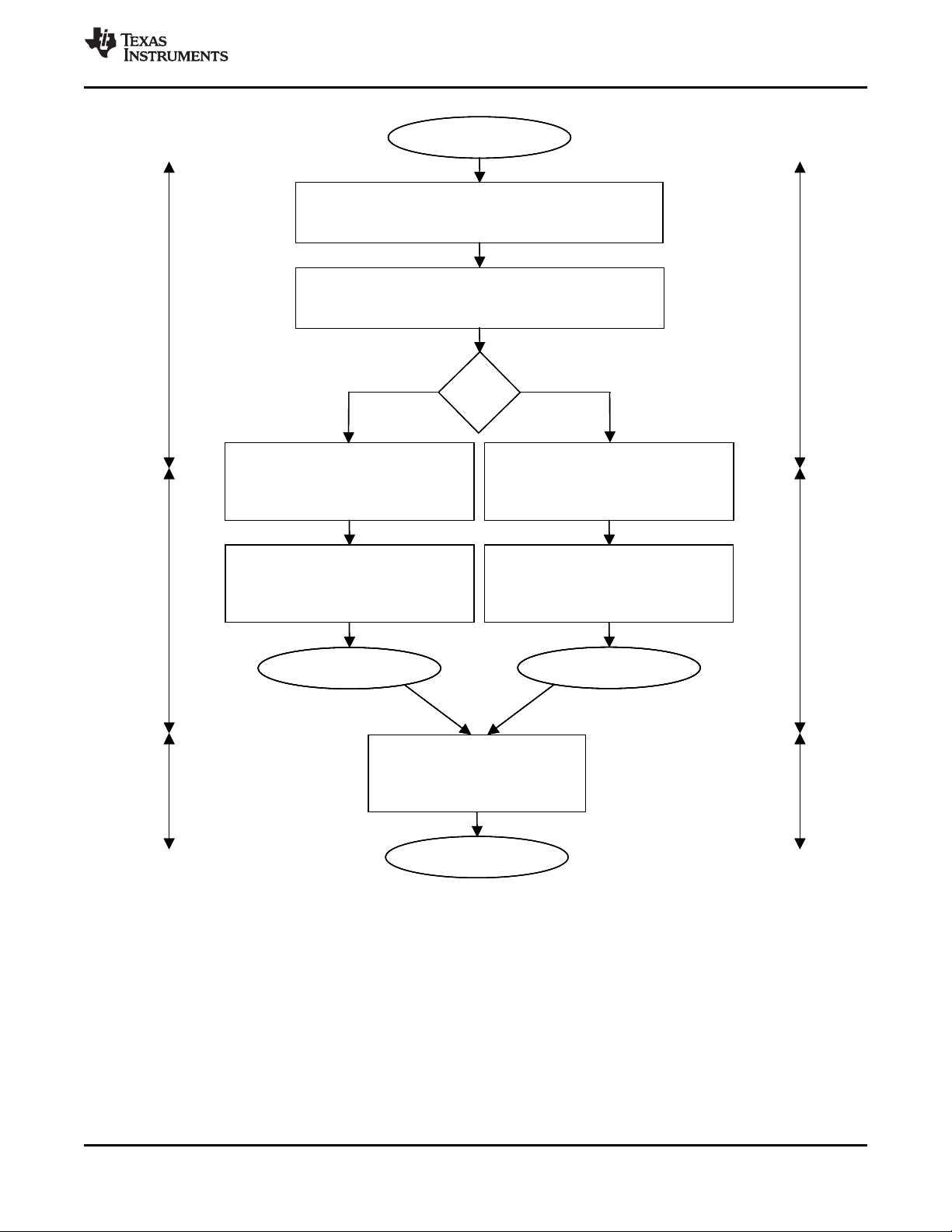
Turn on crystal oscillator core
MAIN: PD_MODE=1, FS_PD=1, XOSC_PD=0, BIAS_PD=1
Wait 1.2 ms*
Power Down mode
*Time to wait depends
on the crystal frequency
and the load capacitance
Wait until lock detected from LOCK pin
or STATUS register
Turn on RX: MAIN: PD_MODE = 0
Wait until lock detected from LOCK pin
or STATUS register
Turn on TX: MAIN: PD_MODE = 0
Set PA_POWER
RX mode
TX mode
Turn off RX/TX:
MAIN: PD_MODE = 1, FS_PD=1,
XOSC_PD=1, BIAS_PD=1
PA_POWER=00h
Power Down mode
Turn on frequency synthesizer
MAIN: RXTX=0, F_REG=0, FS_PD=0
Turn on frequency synthesizer
MAIN: RXTX=1, F_REG=1, FS_PD=0
RX or TX?
RX TX
WakeupCC1020ToRx
SetupCC1020Rx
SetupCC1020PD
WakeupCC1020ToTx
SetupCC1020Tx
SetupCC1020PD
Turn on bias generator. MAIN: BIAS_PD=0
Wait 150 us
Turn on crystal oscillator core
MAIN: PD_MODE=1, FS_PD=1, XOSC_PD=0, BIAS_PD=1
Wait 1.2 ms*
Power Down modePower Down mode
*Time to wait depends
on the crystal frequency
and the load capacitance
Wait until lock detected from LOCK pin
or STATUS register
Turn on RX: MAIN: PD_MODE = 0
Wait until lock detected from LOCK pin
or STATUS register
Turn on TX: MAIN: PD_MODE = 0
Set PA_POWER
Wait until lock detected from LOCK pin
or STATUS register
Turn on RX: MAIN: PD_MODE = 0
Wait until lock detected from LOCK pin
or STATUS register
Turn on TX: MAIN: PD_MODE = 0
Set PA_POWER
RX mode
TX mode
RX modeRX mode
TX modeTX mode
Turn off RX/TX:
MAIN: PD_MODE = 1, FS_PD=1,
XOSC_PD=1, BIAS_PD=1
PA_POWER=00h
Power Down modePower Down mode
Turn on frequency synthesizer
MAIN: RXTX=0, F_REG=0, FS_PD=0
Turn on frequency synthesizer
MAIN: RXTX=1, F_REG=1, FS_PD=0
Turn on frequency synthesizer
MAIN: RXTX=0, F_REG=0, FS_PD=0
Turn on frequency synthesizer
MAIN: RXTX=1, F_REG=1, FS_PD=0
RX or TX?
RX TX
WakeupCC1020ToRx
SetupCC1020Rx
SetupCC1020PD
WakeupCC1020ToTx
SetupCC1020Tx
SetupCC1020PD
Turn on bias generator. MAIN: BIAS_PD=0
Wait 150 us
www.ti.com
SWRS046H –NOVEMBER 2006–REVISED MARCH 2015
CC1020
Figure 5-28. Sequence for Activating RX or TX Mode
5.15 On-Off Keying (OOK)
The data modulator can also provide OOK (On-Off Keying) modulation. OOK is an ASK (Amplitude Shift
Keying) modulation using 100% modulation depth. OOK modulation is enabled in RX and in TX by setting
TXDEV_M[3:0] = 0000 in the DEVIATION register. An OOK eye diagram is shown in Figure 5-29.
The data demodulator can also perform OOK demodulation. The demodulation is done by comparing the
signal level with the “carrier sense” level (programmed as CS_LEVEL in the VGA4 register). The signal is
then decimated and filtered in the data filter. Data decision and bit synchronization are as for FSK
reception.
Copyright © 2006–2015, Texas Instruments Incorporated Detailed Description 53
Submit Documentation Feedback
Product Folder Links: CC1020
Page 54
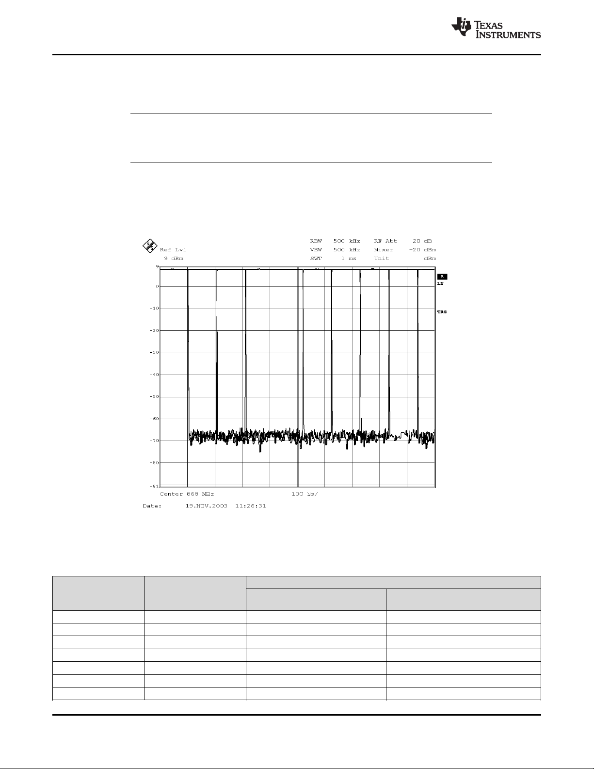
CC1020
SWRS046H –NOVEMBER 2006–REVISED MARCH 2015
In this mode, AGC_AVG in the VGA2 register must be set to 3. The channel bandwidth must be 4 times
the Baud rate for data rates up to 9.6 kBaud. For the highest data rates the channel bandwidth must be 2
times the Baud rate (see Table 5-14). Manchester coding must always be used for OOK.
The automatic frequency control (AFC) cannot be used when receiving OOK, as it requires a
frequency shift.
The AGC has a certain time-constant determined by FILTER_CLK, which depends on the IF filter
bandwidth. There is a lower limit on FILTER_CLK and hence the AGC time constant. For very low data
rates the minimum time constant is too fast and the AGC will increase the gain when a “0” is received and
decrease the gain when a “1” is received. For this reason the minimum data rate in OOK is 2.4 kBaud.
Typical figures for the receiver sensitivity (BER = 10–3) are shown in Table 5-14 for OOK.
www.ti.com
NOTE
9.6 kBaud
Figure 5-29. OOK Eye Diagram
Table 5-14. Typical Receiver Sensitivity as a Function of Data Rate at 433 and 868 MHz, OOK Modulation,
BER = 10–3, Pseudo-random Data (PN9 Sequence)
DATA RATE FILTER BW
[kBaud] [kHz]
2.4 9.6 –116 —
4.8 19.2 –113 –107
9.6 38.4 –103 –104
19.2 51.2 –102 –101
38.4 102.4 –95 –97
76.8 153.6 –92 –94
153.6 307.2 –81 –87
54 Detailed Description Copyright © 2006–2015, Texas Instruments Incorporated
Submit Documentation Feedback
Product Folder Links: CC1020
433 MHz 868 MHz
MANCHESTER MODE MANCHESTER MODE
SENSITIVITY [dBm]
Page 55

C5
C4
XTAL
XOSC_Q1
L parasitic
4 5
1
1 1
C C
= +
+
www.ti.com
5.16 Crystal Oscillator
The recommended crystal frequency is 14.7456 MHz, but any crystal frequency in the range 4 to 20 MHz
can be used. Using a crystal frequency different from 14.7456 MHz might in some applications give
degraded performance. Refer to AN022 Crystal Frequency Selection (SWRA070) for more details on the
use of other crystal frequencies than 14.7456 MHz. The crystal frequency is used as reference for the
data rate (as well as other internal functions) and in the 4 to 20 MHz range the frequencies 4.9152,
7.3728, 9.8304, 12.2880, 14.7456, 17.2032, 19.6608 MHz will give accurate data rates (as shown in
Table 5-4) and an IF frequency of 307.2 kHz. The crystal frequency will influence the programming of the
CLOCK_A, CLOCK_B and MODEM registers.
An external clock signal or the internal crystal oscillator can be used as main frequency reference. An
external clock signal should be connected to XOSC_Q1, while XOSC_Q2 should be left open. The
XOSC_BYPASS bit in the INTERFACE register should be set to ‘1’ when an external digital rail-to-rail
clock signal is used. No DC block should be used then. A sine with smaller amplitude can also be used. A
DC blocking capacitor must then be used (10 nF) and the XOSC_BYPASS bit in the INTERFACE register
should be set to ‘0’. For input signal amplitude, see Section 4.8.
Using the internal crystal oscillator, the crystal must be connected between the XOSC_Q1 and XOSC_Q2
pins. The oscillator is designed for parallel mode operation of the crystal. In addition, loading capacitors
(C4 and C5) for the crystal are required. The loading capacitor values depend on the total load
capacitance, CL, specified for the crystal. The total load capacitance seen between the crystal terminals
should equal CL for the crystal to oscillate at the specified frequency.
CC1020
SWRS046H –NOVEMBER 2006–REVISED MARCH 2015
(33)
The parasitic capacitance is constituted by pin input capacitance and PCB stray capacitance. Total
parasitic capacitance is typically 8 pF. A trimming capacitor may be placed across C5 for initial tuning if
necessary.
The crystal oscillator circuit is shown in Figure 5-30. Typical component values for different values of C
are given in Table 5-15.
The crystal oscillator is amplitude regulated. This means that a high current is required to initiate the
oscillations. When the amplitude builds up, the current is reduced to what is necessary to maintain
approximately 600 mVpp amplitude. This ensures a fast start-up, keeps the drive level to a minimum and
makes the oscillator insensitive to ESR variations. As long as the recommended load capacitance values
are used, the ESR is not critical.
The initial tolerance, temperature drift, aging and load pulling should be carefully specified in order to meet
the required frequency accuracy in a certain application. By specifying the total expected frequency
accuracy in SmartRF Studio together with data rate and frequency separation, the software will estimate
the total bandwidth and compare to the available receiver channel filter bandwidth. The software will report
any contradictions and a more accurate crystal will be recommended if required.
L
Copyright © 2006–2015, Texas Instruments Incorporated Detailed Description 55
Figure 5-30. Crystal Oscillator Circuit
Submit Documentation Feedback
Product Folder Links: CC1020
Page 56

8 7 6 5 4 3 2 1 0
XOR
XOR
Tx out (modulating signal)
Tx data (DIO pin)
8 7 6 5 4 3 2 1 0
XOR
XOR
Rx in (Demodulated Rx data)
Rx out (DIO pin)
CC1020
SWRS046H –NOVEMBER 2006–REVISED MARCH 2015
Table 5-15. Crystal Oscillator Component Values
ITEM CL= 12 pF CL= 16 pF CL= 22 pF
C4 6.8 pF 15 pF 27 pF
C5 6.8 pF 15 pF 27 pF
5.17 Built-in Test Pattern Generator
The CC1020 has a built-in test pattern generator that generates a PN9 pseudo random sequence. The
PN9_ENABLE bit in the MODEM register enables the PN9 generator. A transition on the DIO pin is
required after enabling the PN9 pseudo random sequence.
The PN9 pseudo random sequence is defined by the polynomial x9+ x5+ 1.
The PN9 sequence is ‘XOR’ed with the DIO signal in both TX and RX mode as shown in Figure 5-31.
Hence, by transmitting only zeros (DIO = 0), the BER (Bit Error Rate) can be tested by counting the
number of received ones. Note that the 9 first received bits should be discarded in this case. Also note
that one bit error will generate 3 received ones.
Transmitting only ones (DIO = 1), the BER can be tested by counting the number of received zeroes.
The PN9 generator can also be used for transmission of ‘real-life’ data when measuring narrowband ACP
(Adjacent Channel Power), modulation bandwidth or occupied bandwidth.
www.ti.com
5.18 Interrupt on Pin DCLK
5.18.1 Interrupt Upon PLL Lock
56 Detailed Description Copyright © 2006–2015, Texas Instruments Incorporated
Figure 5-31. PN9 Pseudo-random Sequence Generator in TX and RX Mode
In synchronous mode the DCLK pin on CC1020 can be used to give an interrupt signal to wake the
microcontroller when the PLL is locked.
Submit Documentation Feedback
Product Folder Links: CC1020
Page 57

www.ti.com
PD_MODE[1:0] in the MAIN register should be set to 01. If DCLK_LOCK in the INTERFACE register is set
to 1 the DCLK signal is always logic high if the PLL is not in lock. When the PLL locks to the desired
frequency the DCLK signal changes to logic 0. When this interrupt has been detected write
PD_MODE[1:0] = 00. This will enable the DCLK signal.
This function can be used to wait for the PLL to be locked before the PA is ramped up in transmit mode. In
receive mode, it can be used to wait until the PLL is locked before searching for preamble.
5.18.2 Interrupt Upon Received Signal Carrier Sense
In synchronous mode the DCLK pin on CC1020 can also be used to give an interrupt signal to the
microcontroller when the RSSI level exceeds a certain threshold (carrier sense threshold). This function
can be used to wake or interrupt the microcontroller when a strong signal is received.
Gating the DCLK signal with the carrier sense signal makes the interrupt signal.
This function should only be used in receive mode and is enabled by setting DCLK_CS = 1 in the
INTERFACE register.
The DCLK signal is always logic high unless carrier sense is indicated. When carrier sense is indicated
the DCLK starts running. When gating the DCLK signal with the carrier sense signal at least 2 dummy bits
should be added after the data payload in TX mode. The reason being that the carrier sense signal is
generated earlier in the receive chain (that is, before the demodulator), causing it to be updated 2 bits
before the corresponding data is available on the DIO pin.
CC1020
SWRS046H –NOVEMBER 2006–REVISED MARCH 2015
In transmit mode DCLK_CS must be set to 0. Refer to CC1020 Errata Note 002, available in the CC1020
product folder.
5.19 PA_EN and LNA_EN Digital Output Pins
5.19.1 Interfacing an External LNA or PA
CC1020 has two digital output pins, PA_EN and LNA_EN, which can be used to control an external LNA
or PA. The functionality of these pins are controlled through the INTERFACE register. The outputs can
also be used as general digital output control signals.
EXT_PA_POL and EXT_LNA_POL control the active polarity of the signals.
EXT_PA and EXT_LNA control the function of the pins. If EXT_PA = 1, then the PA_EN pin will be
activated when the internal PA is turned on. Otherwise, the EXT_PA_POL bit controls the PA_EN pin
directly. If EXT_LNA = 1, then the LNA_EN pin will be activated when the internal LNA is turned on.
Otherwise, the EXT_LNA_POL bit controls the LNA_EN pin directly.
These two pins can therefore also be used as two general control signals, see Section 5.19.2. In the TI
reference design LNA_EN and PA_EN are used to control the external T/R switch.
5.19.2 General Purpose Output Control Pins
The two digital output pins, PA_EN and LNA_EN, can be used as two general control signals by setting
EXT_PA = 0 and EXT_LNA = 0. The output value is then set directly by the value written to EXT_PA_POL
and EXT_LNA_POL.
The LOCK pin can also be used as a general-purpose output pin. The LOCK pin is controlled by
LOCK_SELECT[3:0] in the LOCK register. The LOCK pin is low when LOCK_SELECT[3:0] = 0000, and
high when LOCK_SELECT[3:0] = 0001.
These features can be used to save I/O pins on the microcontroller when the other functions associated
with these pins are not used.
Copyright © 2006–2015, Texas Instruments Incorporated Detailed Description 57
Submit Documentation Feedback
Product Folder Links: CC1020
Page 58
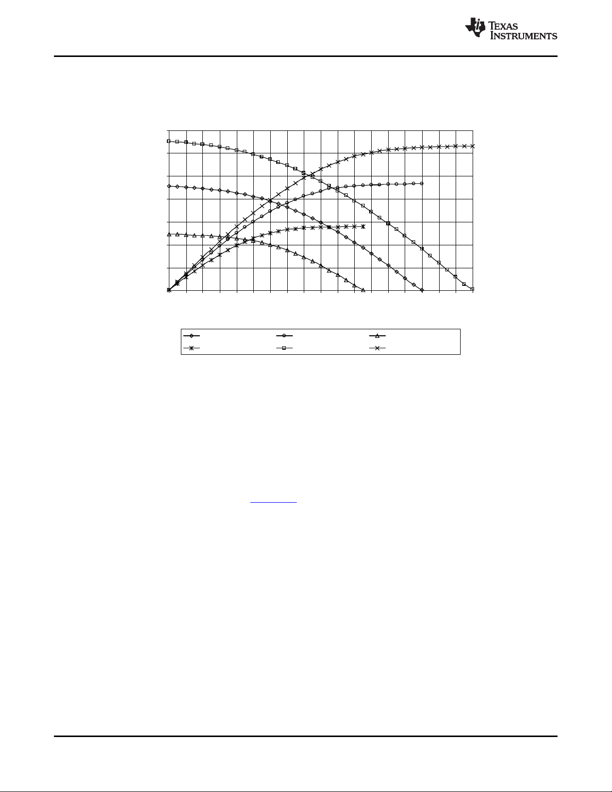
0
200
400
600
800
1000
1200
1400
0
0.2
0.4
0.6
0.8
1
1.2
1.4
1.6
1.8
2
2.2
2.4
2.6
2.8
3
3.2
3.4
3.6
Voltage on PA_EN/LNA_EN pin [V]
Current [uA]
source current, 3 V sink current, 3 V source current, 2.3 V
sink current, 2.3 V source current, 3.6 V sink current, 3.6 V
CC1020
SWRS046H –NOVEMBER 2006–REVISED MARCH 2015
5.19.3 PA_EN and LNA_EN Pin Drive
Figure 5-32 shows the PA_EN and LNA_EN pin drive currents. The sink and source currents have
opposite signs but absolute values are used in Figure 5-32.
www.ti.com
Figure 5-32. Typical PA_EN and LNA_EN Pin Drive
5.20 System Considerations and Guidelines
5.20.1 SRD Regulations
International regulations and national laws regulate the use of radio receivers and transmitters. SRDs
(Short Range Devices) for license free operation are allowed to operate in the 433 and 868 to 870 MHz
bands in most European countries. In the United States, such devices operate in the 260 to 470 and 902
to 928 MHz bands. CC1020 is also applicable for use in the 950 to 960 MHz frequency band in Japan. A
summary of the most important aspects of these regulations can be found in AN001 SRD Regulations For
License Free Transceiver Operation (SWRA090).
5.20.2 Narrowband Systems
CC1020 is specifically designed for narrowband systems complying with ARIB STD-T67 and EN 300 220.
The CC1020 meets the strict requirements to ACP (Adjacent Channel Power) and occupied bandwidth for
a narrowband transmitter. To meet the ARIB STD-T67 requirements, a 3.0 V regulated voltage supply
should be used.
For the receiver side, CC1020 gives very good ACR (Adjacent Channel Rejection), image frequency
suppression and blocking properties for channel spacings down to 12.5 kHz.
Such narrowband performance normally requires the use of external ceramic filters. The CC1020 provides
this performance as a true single-chip solution with integrated IF filters.
Japan and Korea have allocated several frequency bands at 424, 426, 429, 447, 449 and 469 MHz for
narrowband license free operation. CC1020 is designed to meet the requirements for operation in all these
bands, including the strict requirements for narrowband operation down to 12.5 kHz channel spacing.
Due to on-chip complex filtering, the image frequency is removed. An on-chip calibration circuit is used to
get the best possible image rejection. A narrowband preselector filter is not necessary to achieve image
rejection.
58 Detailed Description Copyright © 2006–2015, Texas Instruments Incorporated
Submit Documentation Feedback
Product Folder Links: CC1020
Page 59

www.ti.com
A unique feature in CC1020 is the very fine frequency resolution. This can be used for temperature
compensation of the crystal if the temperature drift curve is known and a temperature sensor is included in
the system. Even initial adjustment can be performed using the frequency programmability. This
eliminates the need for an expensive TCXO and trimming in some applications. For more details refer to
AN027 Temperature Compensation by Indirect Method (SWRA065).
In less demanding applications, a crystal with low temperature drift and low aging could be used without
further compensation. A trimmer capacitor in the crystal oscillator circuit (in parallel with C5) could be used
to set the initial frequency accurately.
The frequency offset between a transmitter and receiver is measured in the CC1020 and can be read
back from the AFC register. The measured frequency offset can be used to calibrate the receiver
frequency using the transmitter as the reference. For more details refer to AN029 CC1020/1021 Automatic
Frequency Control (AFC) (SWRA063).
CC1020 also has the possibility to use Gaussian shaped FSK (GFSK). This spectrum-shaping feature
improves adjacent channel power (ACP) and occupied bandwidth. In ‘true’ FSK systems with abrupt
frequency shifting, the spectrum is inherently broad. By making the frequency shift ‘softer’, the spectrum
can be made significantly narrower. Thus, higher data rates can be transmitted in the same bandwidth
using GFSK.
5.20.3 Low Cost Systems
CC1020
SWRS046H –NOVEMBER 2006–REVISED MARCH 2015
As the CC1020 provides true narrowband multi-channel performance without any external filters, a very
low cost high performance system can be achieved. The oscillator crystal can then be a low cost crystal
with 50 ppm frequency tolerance using the on-chip frequency tuning possibilities.
5.20.4 Battery Operated Systems
In low power applications, the power down mode should be used when CC1020 is not being active.
Depending on the start-up time requirement, the oscillator core can be powered during power down. See
Section 5.14 for information on how effective power management can be implemented.
5.20.5 High Reliability Systems
Using a SAW filter as a preselector will improve the communication reliability in harsh environments by
reducing the probability of blocking. The receiver sensitivity and the output power will be reduced due to
the filter insertion loss. By inserting the filter in the RX path only, together with an external RX/TX switch,
only the receiver sensitivity is reduced and output power is remained. The PA_EN and LNA_EN pin can
be configured to control an external LNA, RX/TX switch or power amplifier. This is controlled by the
INTERFACE register.
Copyright © 2006–2015, Texas Instruments Incorporated Detailed Description 59
Submit Documentation Feedback
Product Folder Links: CC1020
Page 60

CC1020
SWRS046H –NOVEMBER 2006–REVISED MARCH 2015
5.20.6 Frequency Hopping Spread Spectrum Systems (FHSS)
Due to the very fast locking properties of the PLL, the CC1020 is also very suitable for frequency hopping
systems. Hop rates of 1to100 hops/s are commonly used depending on the bit rate and the amount of
data to be sent during each transmission. The two frequency registers (FREQ_A and FREQ_B) are
designed such that the ‘next’ frequency can be programmed while the ‘present’ frequency is used. The
switching between the two frequencies is done through the MAIN register. Several features have been
included to do the hopping without a need to re-synchronize the receiver. For more details, refer to
Application Note AN014 Frequency Hopping Systems (SWRA077).
In order to implement a frequency hopping system with CC1020 do the following:
Set the desired frequency, calibrate and store the following register settings in non-volatile memory:
STATUS1[3:0]: CHP_CURRENT[3:0]
STATUS2[4:0]: VCO_ARRAY[4:0]
TEST1[3:0]: CHP_CO[3:0]
STATUS3[5:0]:VCO_CAL_CURRENT[5:0]
Repeat the calibration for each desired frequency. VCO_CAL_CURRENT[5:0] is not dependent on the RF
frequency and the same value can be used for all frequencies.
When performing frequency hopping, write the stored values to the corresponding TEST1, TEST2 and
TEST3 registers, and enable override:
TEST2[4:0]: VCO_AO[4:0]
TEST2[5]: VCO_OVERRIDE
TEST2[6]: CHP_OVERRIDE
TEST3[5:0]: VCO_CO[5:0]
TEST3[6]: VCO_CAL_OVERRIDE
www.ti.com
CHP_CO[3:0] is the register setting read from CHP_CURRENT[3:0], VCO_AO[4:0] is the register setting
read from VCO_ARRAY[4:0] and VCO_CO[5:0] is the register setting read from
VCO_CAL_CURRENT[5:0].
Assume channel 1 defined by register FREQ_A is currently being used and that CC1020 should operate
on channel 2 next (to change channel simply write to register MAIN[6]). The channel 2 frequency can be
set by register FREQ_B which can be written to while operating on channel 1. The calibration data must
be written to the TEST1-3 registers after switching to the next frequency. That is, when hopping to a new
channel write to register MAIN[6] first and the test registers next. The PA should be switched off between
each hop and the PLL should be checked for lock before switching the PA back on after a hop has been
performed.
NOTE
The override bits VCO_OVERRIDE, CHP_OVERRIDE and VCO_CAL_OVERRIDE must be
disabled when performing a re-calibration.
60 Detailed Description Copyright © 2006–2015, Texas Instruments Incorporated
Submit Documentation Feedback
Product Folder Links: CC1020
Page 61

7125
=
lll
l
www.ti.com
5.21 Antenna Considerations
CC1020 can be used together with various types of antennas. The most common antennas for shortrange communication are monopole, helical and loop antennas.
Monopole antennas are resonant antennas with a length corresponding to one quarter of the electrical
wavelength ( ). They are very easy to design and can be implemented simply as a “piece of wire” or
even integrated onto the PCB.
Non-resonant monopole antennas shorter than can also be used, but at the expense of range. In size
and cost critical applications such an antenna may very well be integrated onto the PCB.
Helical antennas can be thought of as a combination of a monopole and a loop antenna. They are a good
compromise in size critical applications. But helical antennas tend to be more difficult to optimize than the
simple monopole.
Loop antennas are easy to integrate into the PCB, but are less effective due to difficult impedance
matching because of their very low radiation resistance.
For low power applications the monopole antenna is recommended due to its simplicity as well as
providing the best range.
CC1020
SWRS046H –NOVEMBER 2006–REVISED MARCH 2015
The length of the monopole antenna is given by Equation 34.
(34)
Where:
f is in MHz, giving the length in cm.
An antenna for 868 MHz should be 8.2 cm, and 16.4 cm for 433 MHz.
The antenna should be connected as close as possible to the IC. If the antenna is located away from the
input pin the antenna should be matched to the feeding transmission line (50 Ω).
For a more thorough background on antennas, please refer to AN003 SRD Antennas (SWRA088).
Copyright © 2006–2015, Texas Instruments Incorporated Detailed Description 61
Submit Documentation Feedback
Product Folder Links: CC1020
Page 62

CC1020
SWRS046H –NOVEMBER 2006–REVISED MARCH 2015
5.22 Configuration Registers
The configuration of CC1020 is done by programming the 8-bit configuration registers. The configuration
data based on selected system parameters are most easily found by using the SmartRF Studio software.
Complete descriptions of the registers are given in Section 5.22.1. After a RESET is programmed, all the
registers have default values. The TEST registers also get default values after a RESET, and should not
be altered by the user.
TI recommends using the register settings found using the SmartRF Studio software. These are the
register settings that TI specifies across temperature, voltage, and process. Check the TI web site for
regularly updates to the SmartRF Studio software.
Table 5-16. CC1020 Register Overview
ADDRESS ACRONYM REGISTER NAME
00h MAIN Main control register
01h INTERFACE Interface control register
02h RESET Digital module reset register
03h SEQUENCING Automatic power-up sequencing control register
04h FREQ_2A Frequency register 2A
05h FREQ_1A Frequency register 1A
06h FREQ_0A Frequency register 0A
07h CLOCK_A Clock generation register A
08h FREQ_2B Frequency register 2B
09h FREQ_1B Frequency register 1B
0Ah FREQ_0B Frequency register 0B
0Bh CLOCK_B Clock generation register B
0Ch VCO VCO current control register
0Dh MODEM Modem control register
0Eh DEVIATION TX frequency deviation register
0Fh AFC_CONTROL RX AFC control register
10h FILTER Channel filter / RSSI control register
11h VGA1 VGA control register 1
12h VGA2 VGA control register 2
13h VGA3 VGA control register 3
14h VGA4 VGA control register 4
15h LOCK Lock control register
16h FRONTEND Front end bias current control register
17h ANALOG Analog modules control register
18h BUFF_SWING LO buffer and prescaler swing control register
19h BUFF_CURRENT LO buffer and prescaler bias current control register
1Ah PLL_BW PLL loop bandwidth / charge pump current control register
1Bh CALIBRATE PLL calibration control register
1Ch PA_POWER Power amplifier output power register
1Dh MATCH
1Eh PHASE_COMP Phase error compensation control register for LO I/Q
1Fh GAIN_COMP Gain error compensation control register for mixer I/Q
20h POWERDOWN Power-down control register
21h TEST1 Test register for overriding PLL calibration
22h TEST2 Test register for overriding PLL calibration
23h TEST3 Test register for overriding PLL calibration
24h TEST4 Test register for charge pump and IF chain testing
Match capacitor array control register, for RX and TX impedance
matching
www.ti.com
62 Detailed Description Copyright © 2006–2015, Texas Instruments Incorporated
Submit Documentation Feedback
Product Folder Links: CC1020
Page 63
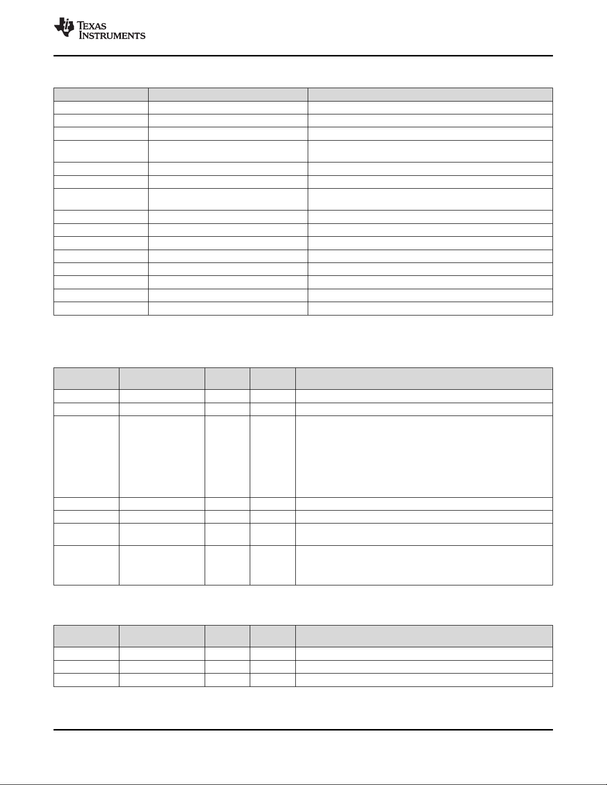
www.ti.com
SWRS046H –NOVEMBER 2006–REVISED MARCH 2015
Table 5-16. CC1020 Register Overview (continued)
ADDRESS ACRONYM REGISTER NAME
25h TEST5 Test register for ADC testing
26h TEST6 Test register for VGA testing
27h TEST7 Test register for VGA testing
40h STATUS
41h RESET_DONE Status register for digital module reset
42h RSSI Received signal strength register
43h AFC
44h GAUSS_FILTER Digital FM demodulator register
45h STATUS1 Status of PLL calibration results and so on (test only)
46h STATUS2 Status of PLL calibration results and so on (test only)
47h STATUS3 Status of PLL calibration results and so on (test only)
48h STATUS4 Status of ADC signals (test only)
49h STATUS5 Status of channel filter “I” signal (test only)
4Ah STATUS6 Status of channel filter “Q” signal (test only)
4Bh STATUS7 Status of AGC (test only)
Status information register (PLL lock, RSSI, calibration ready, and
so on)
Average received frequency deviation from IF (can be used for
AFC)
CC1020
5.22.1 Memory
Table 5-17. MAIN Register (00h)
REGISTER NAME ACTIVE DESCRIPTION
MAIN[7] RXTX — — RX/TX switch, 0: RX , 1: TX
MAIN[6] F_REG — — Selection of Frequency Register, 0: Register A, 1: Register B
MAIN[5:4] PD_MODE[1:0] — — Power down mode
MAIN[3] FS_PD — H Power Down of Frequency Synthesizer
MAIN[2] XOSC_PD — H Power Down of Crystal Oscillator Core
MAIN[1] BIAS_PD — H Power Down of BIAS (Global Current Generator) and Crystal Oscillator
MAIN[0] RESET_N — L Reset, active low. Writing RESET_N low will write default values to all
Table 5-18. MAIN Register (00h) When Using Automatic Power-up Sequencing
DEFAULT
VALUE
0 (00): Receive Chain in power-down in TX, PA in power-down in
RX
1 (01): Receive Chain and PA in power down in both TX and RX
2 (10): Individual modules can be put in power down by
programming the POWERDOWN register
3 (11): Automatic power-up sequencing is activated
(see Table 5-18)
Buffer
other registers than MAIN. Bits in MAIN do not have a default value
and will be written directly through the configuration interface. Must be
set high to complete reset.
(RXTX = 0, PD_MODE[1:0] =11)
REGISTER NAME ACTIVE DESCRIPTION
MAIN[7] RXTX — — Automatic power-up sequencing only works in RX (RXTX=0)
MAIN[6] F_REG — — Selection of Frequency Register, 0: Register A, 1: Register B
MAIN[5:4] PD_MODE[1:0] — H Set PD_MODE[1:0]=3 (11) to enable sequencing
Copyright © 2006–2015, Texas Instruments Incorporated Detailed Description 63
DEFAULT
VALUE
Submit Documentation Feedback
Product Folder Links: CC1020
Page 64
CC1020
SWRS046H –NOVEMBER 2006–REVISED MARCH 2015
Table 5-18. MAIN Register (00h) When Using Automatic Power-up Sequencing
(RXTX = 0, PD_MODE[1:0] =11) (continued)
REGISTER NAME ACTIVE DESCRIPTION
MAIN[3:2] SEQ_CAL[1:0] — — Controls PLL calibration before re-entering power down
MAIN[1] SEQ_PD — ↑ ↑1: Put the chip in power down and wait for start of new power-up
MAIN[0] RESET_N — L Reset, active low. Writing RESET_N low will write default values to all
DEFAULT
VALUE
0: Never perform PLL calibration as part of sequence
1: Always perform PLL calibration at end of sequence
2: Perform PLL calibration at end of every 16th sequence
3: Perform PLL calibration at end of every 256th sequence
sequence
other registers than MAIN. Bits in MAIN do not have a default value
and will be written directly through the configuration interface. Must be
set high to complete reset.
www.ti.com
Table 5-19. INTERFACE Register (01h)
REGISTER NAME ACTIVE DESCRIPTION
INTERFACE[7] XOSC_BYPASS 0 H Bypass internal crystal oscillator, use external clock
INTERFACE[6] SEP_DI_DO 0 H Use separate pin for RX data output
INTERFACE[5] DCLK_LOCK 0 H Gate DCLK signal with PLL lock signal in synchronous mode
INTERFACE[4] DCLK_CS 0 H Gate DCLK signal with carrier sense indicator in synchronous mode
INTERFACE[3] EXT_PA 0 H Use PA_EN pin to control external PA
INTERFACE[2] EXT_LNA 0 H Use LNA_EN pin to control external LNA
INTERFACE[1] EXT_PA_POL 0 H Polarity of external PA control
INTERFACE[0] EXT_LNA_POL 0 H Polarity of external LNA control
(1) If TF_ENABLE=1 or TA_ENABLE=1 in TEST4 register, then INTERFACE[3:0] controls analog test module: INTERFACE[3] = TEST_PD,
INTERFACE[2:0] = TEST_MODE[2:0]. Otherwise, TEST_PD=1 and TEST_MODE[2:0]=001.
DEFAULT
VALUE
0: Internal crystal oscillator is used, or external sine wave fed
through a coupling capacitor
1: Internal crystal oscillator in power down, external clock with railto-rail swing is used
0: DIO is data output in RX and data input in TX. LOCK pin is
available (Normal operation).
1: DIO is always input, and a separate pin is used for RX data
output (synchronous mode: LOCK pin, asynchronous mode: DCLK
pin).
If SEP_DI_DO=1 and SEQ_PSEL=0 in SEQUENCING register then
negative transitions on DIO is used to start power-up sequencing when
PD_MODE=3 (power-up sequencing is enabled).
Only applies when PD_MODE = "01"
0: DCLK is always 1
1: DCLK is always 1 unless PLL is in lock
Use when receive chain is active (in power up)
Always set to 0 in TX mode.
0: DCLK is independent of carrier sense indicator.
1: DCLK is always 1 unless carrier sense is indicated
0: PA_EN pin always equals EXT_PA_POL bit
1: PA_EN pin is asserted when internal PA is turned on
0: LNA_EN pin always equals EXT_LNA_POL bit
1: LNA_EN pin is asserted when internal LNA is turned on
0: PA_EN pin is "0" when activating external PA
1: PA_EN pin is “1” when activating external PA
0: LNA_EN pin is “0” when activating external LNA
1: LNA_EN pin is “1” when activating external LNA
(1)
64 Detailed Description Copyright © 2006–2015, Texas Instruments Incorporated
Submit Documentation Feedback
Product Folder Links: CC1020
Page 65

www.ti.com
CC1020
SWRS046H –NOVEMBER 2006–REVISED MARCH 2015
Table 5-20. RESET Register (02h)
REGISTER NAME ACTIVE DESCRIPTION
RESET[7] ADC_RESET_N 0 L Reset ADC control logic
RESET[6] AGC_RESET_N 0 L Reset AGC (VGA control) logic
RESET[5] GAUSS_RESET_N 0 L Reset Gaussian data filter
RESET[4] AFC_RESET_N 0 L Reset AFC / FSK decision level logic
RESET[3] BITSYNC_RESET_N 0 L Reset modulator, bit synchronization logic and PN9 PRBS generator
RESET[2] SYNTH_RESET_N 0 L Reset digital part of frequency synthesizer
RESET[1] SEQ_RESET_N 0 L Reset power-up sequencing logic
RESET[0] CAL_LOCK_RESET_N 0 L Reset calibration logic and lock detector
(1) For reset of CC1020 write RESET_N=0 in the MAIN register. The reset register should not be used during normal operation.
(2) Bits in the RESET register are self-clearing (will be set to 1 when the reset operation starts). Relevant digital clocks must be running for
the resetting to complete. After writing to the RESET register, the user should verify that all reset operations have been completed, by
reading the RESET_DONE status register (41h) until all bits equal 1.
DEFAULT
VALUE
(1)(2)
Table 5-21. SEQUENCING Register (03h)
REGISTER NAME ACTIVE DESCRIPTION
SEQUENCING[7] SEQ_PSEL 1 H Use PSEL pin to start sequencing
SEQUENCING[6:4] RX_WAIT[2:0] 0 — Waiting time from PLL enters lock until RX power up
SEQUENCING[3:0] CS_WAIT[3:0] 10 — Waiting time for carrier sense from RX power up
DEFAULT
VALUE
0: PSEL pin does not start sequencing. Negative transitions on
DIO starts power-up sequencing if SEP_DI_DO=1.
1: Negative transitions on the PSEL pin will start power-up
sequencing
0: Wait for approx. 32 ADC_CLK periods (26 μs)
1: Wait for approx. 44 ADC_CLK periods (36 μs)
2: Wait for approx. 64 ADC_CLK periods (52 μs)
3: Wait for approx. 88 ADC_CLK periods (72 μs)
4: Wait for approx. 128 ADC_CLK periods (104 μs)
5: Wait for approx. 176 ADC_CLK periods (143 μs)
6: Wait for approx. 256 ADC_CLK periods (208 μs)
7: No additional waiting time before RX power up
0: Wait 20 FILTER_CLK periods before power down 1: Wait 22
FILTER_CLK periods before power down
2: Wait 24 FILTER_CLK periods before power down
3: Wait 26 FILTER_CLK periods before power down
4: Wait 28 FILTER_CLK periods before power down
5: Wait 30 FILTER_CLK periods before power down
6: Wait 32 FILTER_CLK periods before power down
7: Wait 36 FILTER_CLK periods before power down
8: Wait 40 FILTER_CLK periods before power down
9: Wait 44 FILTER_CLK periods before power down
10: Wait 48 FILTER_CLK periods before power down
11: Wait 52 FILTER_CLK periods before power down
12: Wait 56 FILTER_CLK periods before power down
13: Wait 60 FILTER_CLK periods before power down
14: Wait 64 FILTER_CLK periods before power down
15: Wait 72 FILTER_CLK periods before power down
Table 5-22. FREQ_2A Register (04h)
REGISTER NAME ACTIVE DESCRIPTION
FREQ_2A[7:0] FREQ_A[22:15] 131 — 8 MSB of frequency control word A
Copyright © 2006–2015, Texas Instruments Incorporated Detailed Description 65
DEFAULT
VALUE
Submit Documentation Feedback
Product Folder Links: CC1020
Page 66

CC1020
SWRS046H –NOVEMBER 2006–REVISED MARCH 2015
Table 5-23. FREQ_1A Register (05h)
www.ti.com
REGISTER NAME ACTIVE DESCRIPTION
FREQ_1A[7:0] FREQ_1A[7:0] 177 — Bit 15 to 8 of frequency control word A
DEFAULT
VALUE
Table 5-24. FREQ_0A Register (06h)
REGISTER NAME ACTIVE DESCRIPTION
FREQ_0A[7:1] FREQ_A[6:0] 124 — 7 LSB of frequency control word A
FREQ_0A[0] DITHER_A 1 H Enable dithering for frequency A
DEFAULT
VALUE
Table 5-25. CLOCK_A Register (07h)
REGISTER NAME ACTIVE DESCRIPTION
CLOCK_A[7:5] REF_DIV_A[2:0] 2 — Reference frequency divisor (A):
CLOCK_A[4:2] MCLK_DIV1_A[2:0] 4 — Modem clock divider 1 (A):
CLOCK_A[1:0] MCLK_DIV2_A[1:0] 0 — Modem clock divider 2 (A):
DEFAULT
VALUE
0: Not supported
1: REF_CLK frequency = Crystal frequency / 2
…
7: REF_CLK frequency = Crystal frequency / 8
It is recommended to use the highest possible reference clock
frequency that allows the desired Baud rate.
0: Divide by 2.5
1: Divide by 3
2: Divide by 4
3: Divide by 7.5 (2.5 × 3)
4: Divide by 12.5 (2.5 × 5)
5: Divide by 40 (2.5 × 16)
6: Divide by 48 (3 × 16)
7: Divide by 64 (4 × 16)
0: Divide by 1
1: Divide by 2
2: Divide by 4
3: Divide by 8
MODEM_CLK frequency is FREF frequency divided by the product of
divider 1 and divider 2.
Baud rate is MODEM_CLK frequency divided by 8.
Table 5-26. FREQ_2B Register (08h)
REGISTER NAME ACTIVE DESCRIPTION
FREQ_2B[7:0] FREQ_B[22:15] 131 — 8 MSB of frequency control word B
DEFAULT
VALUE
Table 5-27. FREQ_1B Register (09h)
REGISTER NAME ACTIVE DESCRIPTION
FREQ_1B[7:0] FREQ_B[14:7] 189 — 8 MSB of frequency control word B
66 Detailed Description Copyright © 2006–2015, Texas Instruments Incorporated
DEFAULT
VALUE
Submit Documentation Feedback
Product Folder Links: CC1020
Page 67

www.ti.com
CC1020
SWRS046H –NOVEMBER 2006–REVISED MARCH 2015
Table 5-28. FREQ_0B Register (0Ah)
REGISTER NAME ACTIVE DESCRIPTION
FREQ_0B[7:1] FREQ_B[6:0] 124 — 7 LSB of frequency control word B
FREQ_0B[0] DITHER_B 1 H Enable dithering for frequency B
DEFAULT
VALUE
Table 5-29. CLOCK_B Register (0Bh)
REGISTER NAME ACTIVE DESCRIPTION
CLOCK_B[7:5] REF_DIV_B[2:0] 2 — Reference frequency divisor (B):
CLOCK_B[4:2] MCLK_DIV1_B[2:0] 4 — Modem clock divider 1 (B):
CLOCK_B[1:0] MCLK_DIV2_B[1:0] 0 — Modem clock divider 2 (B):
DEFAULT
VALUE
0: Not supported
1: REF_CLK frequency = Crystal frequency / 2
…
7: REF_CLK frequency = Crystal frequency / 8
0: Divide by 2.5
1: Divide by 3
2: Divide by 4
3: Divide by 7.5 (2.5 × 3)
4: Divide by 12.5 (2.5 × 5)
5: Divide by 40 (2.5 × 16)
6: Divide by 48 (3 × 16)
7: Divide by 64 (4 × 16)
0: Divide by 1
1: Divide by 2
2: Divide by 4
3: Divide by 8
MODEM_CLK frequency is FREF frequency divided by the product of
divider 1 and divider 2.
Baud rate is MODEM_CLK frequency divided by 8.
Table 5-30. VCO Register (0Ch)
REGISTER NAME ACTIVE DESCRIPTION
VCO[7:4] VCO_CURRENT_A[3:0] 8 — Control of current in VCO core for frequency A
VCO[3:0] VCO_CURRENT_B[3:0] 8 —
DEFAULT
VALUE
0 : 1.4 mA current in VCO core
1 : 1.8 mA current in VCO core
2 : 2.1 mA current in VCO core
3 : 2.5 mA current in VCO core
4 : 2.8 mA current in VCO core
5 : 3.2 mA current in VCO core
6 : 3.5 mA current in VCO core
7 : 3.9 mA current in VCO core
8 : 4.2 mA current in VCO core
9 : 4.6 mA current in VCO core
10 : 4.9 mA current in VCO core
11 : 5.3 mA current in VCO core
12 : 5.6 mA current in VCO core
13 : 6.0 mA current in VCO core
14 : 6.4 mA current in VCO core
15 : 6.7 mA current in VCO core
Recommended setting: VCO_CURRENT_A=4
Control of current in VCO core for frequency B
The current steps are the same as for VCO_CURRENT_A
Recommended setting: VCO_CURRENT_B=4
Copyright © 2006–2015, Texas Instruments Incorporated Detailed Description 67
Submit Documentation Feedback
Product Folder Links: CC1020
Page 68
CC1020
SWRS046H –NOVEMBER 2006–REVISED MARCH 2015
Table 5-31. MODEM Register (0Dh)
www.ti.com
REGISTER NAME ACTIVE DESCRIPTION
DEFAULT
VALUE
MODEM[7] — 0 — Reserved, write 0
MODEM[6:4] ADC_DIV[2:0] 3 — ADC clock divisor
(1)
0: Not supported
1: ADC frequency = XOSC frequency / 4
2: ADC frequency = XOSC frequency / 6
3: ADC frequency = XOSC frequency / 8
4: ADC frequency = XOSC frequency / 10
5: ADC frequency = XOSC frequency / 12
6: ADC frequency = XOSC frequency / 14
7: ADC frequency = XOSC frequency / 16
MODEM[3] — 0 — Reserved, write 0
MODEM[2] PN9_ENABLE 0 H Enable scrambling of TX and RX with PN9 pseudo-random bit
sequence
0: PN9 scrambling is disabled
1: PN9 scrambling is enabled (x9+ x5+ 1)
The PN9 pseudo-random bit sequence can be used for BER testing by
only transmitting zeros, and then counting the number of received
ones.
MODEM[1:0] DATA_FORMAT[1:0] 0 — Modem data format
0 (00): NRZ operation
1 (01): Manchester operation
2 (10): Transparent asynchronous UART operation, set DCLK=0
3 (11): Transparent asynchronous UART operation, set DCLK=1
(1) The intermediate frequency should be as close to 307.2 kHz as possible. ADC clock frequency is always 4 times the intermediate
frequency and should therefore be as close to 1.2288 MHz as possible.
Table 5-32. DEVIATION Register (0Eh)
REGISTER NAME ACTIVE DESCRIPTION
DEVIATION[7] TX_SHAPING 1 H Enable Gaussian shaping of transmitted data
DEVIATION[6:4] TXDEV_X[2:0] 6 — Transmit frequency deviation exponent
DEVIATION [3:0] TXDEV_M[3:0] 8 — Transmit frequency deviation mantissa
DEFAULT
VALUE
Recommended setting: TX_SHAPING=1
Deviation in 402 to 470 MHz band:
F
× XDEV_M × 2
REF
(TXDEV_X−16)
Deviation in 804 to 960 MHz band:
F
× TXDEV_M × 2
REF
(TXDEV_X−15)
On-off-keying (OOK) is used in RX/TX if TXDEV_M[3:0]=0
To find TXDEV_M given the deviation and TXDEV_X:
TXDEV_M = deviation × 2
(16−TXDEV_X)
in 402 to 470 MHz band,
TXDEV_M = deviation × 2
(15−TXDEV_X)
in 804 to 960 MHz band,
Decrease TXDEV_X and try again if TXDEV_M < 8.
Increase TXDEV_X and try again if TXDEV_M ≥ 16.
/ F
REF
/ F
REF
68 Detailed Description Copyright © 2006–2015, Texas Instruments Incorporated
Submit Documentation Feedback
Product Folder Links: CC1020
Page 69
www.ti.com
CC1020
SWRS046H –NOVEMBER 2006–REVISED MARCH 2015
Table 5-33. AFC_CONTROL Register (0Fh)
REGISTER NAME ACTIVE DESCRIPTION
DEFAULT
VALUE
(1)
AFC_CONTROL[7:6] SETTLING[1:0] 2 — Controls AFC settling time versus accuracy
0: AFC off; zero average frequency is used in demodulator
1: Fastest settling; frequency averaged over 1 0/1 bit pair
2: Medium settling; frequency averaged over 2 0/1 bit pairs
3: Slowest settling; frequency averaged over 4 0/1 bit pairs
Recommended setting:
AFC_CONTROL=3 for higher accuracy unless it is essential to
have the fastest settling time when transmission starts after RX
is activated.
AFC_CONTROL[5:4] RXDEV_X[1:0] 1 — RX frequency deviation exponent
AFC_CONTROL[3:0] RXDEV_M[3:0] 12 — RX frequency deviation mantissa
Expected RX deviation should be:
Baud rate × RXDEV_M × 2
(RXDEV_X−3)
/ 3
To find RXDEV_M given the deviation and RXDEV_X:
RXDEV_M = 3 × deviation × 2
(3−RXDEV_X)
/ Baud rate
Decrease RXDEV_X and try again if RXDEV_M < 8.
Increase RXDEV_X and try again if RXDEV_M ≥ 16.
(1) The RX frequency deviation should be close to half the TX frequency deviation for GFSK at 100 kBaud data rate and below. The RX
frequency deviation should be close to the TX frequency deviation for FSK and for GFSK at 100 kBaud data rate and above.
Table 5-34. FILTER Register (10h)
REGISTER NAME ACTIVE DESCRIPTION
DEFAULT
VALUE
FILTER[7] FILTER_BYPASS 0 H Bypass analog image rejection / anti-alias filter. Set to 1 for increased
dynamic range at high Baud rates.
Recommended setting:
FILTER_BYPASS=0 below 76.8 kBaud,
FILTER_BYPASS=1 for 76.8 kBaud and up.
FILTER[6:5] DEC_SHIFT[1:0] 0 — Number of extra bits to shift decimator input (may improve filter
accuracy and lower power consumption).
Recommended settings:
DEC_SHIFT=0 when DEC_DIV ≤1
(receiver channel bandwidth ≥ 153.6 kHz),
DEC_SHIFT=1 when optimized sensitivity and 1< DEC_DIV <
24
(12.29 kHz < receiver channel bandwidth < 153.6 kHz),
DEC_SHIFT=2 when optimized selectivity and DEC_DIV ≥ 24
(receiver channel bandwidth ≤12.29 kHz)
FILTER[4:0] DEC_DIV[4:0] 0 — Decimation clock divisor
0: Decimation clock divisor = 1, 307.2 kHz channel filter BW.
1: Decimation clock divisor = 2, 153.6 kHz channel filter BW.
…
30: Decimation clock divisor = 31, 9.91 kHz channel filter BW.
31: Decimation clock divisor = 32, 9.6 kHz channel filter BW.
Channel filter bandwidth is 307.2 kHz divided by the decimation clock
divisor.
Copyright © 2006–2015, Texas Instruments Incorporated Detailed Description 69
Submit Documentation Feedback
Product Folder Links: CC1020
Page 70
CC1020
SWRS046H –NOVEMBER 2006–REVISED MARCH 2015
www.ti.com
Table 5-35. VGA1 Register (11h)
REGISTER NAME ACTIVE DESCRIPTION
VGA1[7:6] CS_SET[1:0] 1 — Sets the number of consecutive samples at or above carrier sense
VGA1[5] CS_RESET 1 — Sets the number of consecutive samples below carrier sense level
VGA1[4:2] VGA_WAIT[2:0] 1 — Controls how long AGC, bit synchronization, AFC and RSSI levels are
VGA1[1:0] VGA_FREEZE[1:0] 1 — Controls the additional time AGC, bit synchronization, AFC and RSSI
DEFAULT
VALUE
level before carrier sense is indicated (for example, on LOCK pin)
0: Set carrier sense after first sample at or above carrier sense
level
1: Set carrier sense after second sample at or above carrier sense
level
2: Set carrier sense after third sample at or above carrier sense
level
3: Set carrier sense after fourth sample at or above carrier sense
level
Increasing CS_SET reduces the number of “false” carrier sense events
due to noise at the expense of increased carrier sense response time.
before carrier sense indication (for example, on lock pin) is reset
0: Carrier sense is reset after first sample below carrier sense level
1: Carrier sense is reset after second sample below carrier sense
level
Recommended setting: CS_RESET=1 in order to reduce the chance of
losing carrier sense due to noise.
frozen after VGA gain is changed when frequency is changed between
A and B or PLL has been out of lock or after RX power up
0: Freeze operation for 16 filter clocks, 8/(filter BW) seconds
1: Freeze operation for 20 filter clocks, 10/(filter BW) seconds
2: Freeze operation for 24 filter clocks, 12/(filter BW) seconds
3: Freeze operation for 28 filter clocks, 14/(filter BW) seconds
4: Freeze operation for 32 filter clocks, 16/(filter BW) seconds
5: Freeze operation for 40 filter clocks, 20/(filter BW) seconds
6: Freeze operation for 48 filter clocks, 24/(filter BW) seconds
7: Freeze present levels unconditionally
levels are frozen when frequency is changed between A and B or PLL
has been out of lock or after RX power up
0: Freeze levels for approx. 16 ADC_CLK periods (13 µs)
1: Freeze levels for approx. 32 ADC_CLK periods (26 µs)
2: Freeze levels for approx. 64 ADC_CLK periods (52 µs)
3: Freeze levels for approx. 128 ADC_CLK periods (104 µs)
70 Detailed Description Copyright © 2006–2015, Texas Instruments Incorporated
Submit Documentation Feedback
Product Folder Links: CC1020
Page 71
www.ti.com
CC1020
SWRS046H –NOVEMBER 2006–REVISED MARCH 2015
Table 5-36. VGA2 Register (12h)
REGISTER NAME ACTIVE DESCRIPTION
VGA2[7] LNA2_MIN 0 — Minimum LNA2 setting used in VGA
VGA2[6] LNA2_MAX 1 — Maximum LNA2 setting used in VGA
VGA2[5:4] LNA2_SETTING[1:0] 3 — Selects at what VGA setting the LNA gain should be changed
VGA2[3] AGC_DISABLE 0 H Disable AGC
VGA2[2] AGC_HYSTERESIS 1 H Enable AGC hysteresis
VGA2[1:0] AGC_AVG[1:0] 1 — Sets how many samples that are used to calculate average output
DEFAULT
VALUE
0: Minimum LNA2 gain
1: Medium LNA2 gain
Recommended setting: LNA2_MIN=0 for best selectivity.
0: Medium LNA2 gain
1: Maximum LNA2 gain
Recommended setting: LNA2_MAX=1 for best sensitivity.
0: Apply LNA2 change below min. VGA setting.
1: Apply LNA2 change at approx. 1/3 VGA setting (around VGA
setting 10).
2: Apply LNA2 change at approx. 2/3 VGA setting (around VGA
setting 19).
3: Apply LNA2 change above max. VGA setting.
Recommended setting:
LNA2_SETTING=0 if VGA_SETTING<10, LNA2_SETTING=1
otherwise.
If LNA2_MIN=1 and LNA2_MAX=0, then the LNA2 setting is
controlled by LNA2_SETTING:
0: Between medium and maximum LNA2 gain
1: Minimum LNA2 gain
2: Medium LNA2 gain
3: Maximum LNA2 gain
0: AGC is enabled
1: AGC is disabled (VGA_SETTING determines VGA gain)
Recommended setting: AGC_DISABLE=0 for good dynamic range.
0: No hysteresis. Immediate gain change for smallest up/down
step
1: Hysteresis enabled. Two samples in a row must indicate gain
change for smallest up or down step
Recommended setting: AGC_HYSTERESIS=1.
magnitude for AGC/RSSI.
0: Magnitude is averaged over 2 filter output samples
1: Magnitude is averaged over 4 filter output samples
2: Magnitude is averaged over 8 filter output samples
3: Magnitude is averaged over 16 filter output samples
Recommended setting: AGC_AVG=1.
For best AGC/RSSI accuracy AGC_AVG=3.
For automatic power-up sequencing, the AGC_AVG and CS_SET
values must be chosen so that carrier sense is available in time to be
detected before the chip re-enters power down.
Copyright © 2006–2015, Texas Instruments Incorporated Detailed Description 71
Submit Documentation Feedback
Product Folder Links: CC1020
Page 72

CC1020
SWRS046H –NOVEMBER 2006–REVISED MARCH 2015
www.ti.com
Table 5-37. VGA3 Register (13h)
REGISTER NAME ACTIVE DESCRIPTION
VGA3[7:5] VGA_DOWN[2:0] 1 — Decides how much the signal strength must be above
VGA3[4:0] VGA_SETTING[4:0] 24 H VGA setting to be used when receive chain is turned on
DEFAULT
VALUE
CS_LEVEL+VGA_UP before VGA gain is decreased. Based on the
calculated internal strength level, which has an LSB resolution of 1.5
dB.
0: Gain is decreased when level is above CS_LEVEL+ 8 +
VGA_UP + 3
1: Gain is decreased when level is above CS_LEVEL+ 8 +
VGA_UP + 4
…
6: Gain is decreased when level is above CS_LEVEL+ 8 +
VGA_UP + 9
7: Gain is decreased when level is above CS_LEVEL+ 8 +
VGA_UP + 10
See Figure 5-15 for an explanation of the relationship between RSSI,
AGC and carrier sense settings.
This is also the maximum gain that the AGC is allowed to use.
See Figure 5-15 for an explanation of the relationship between RSSI,
AGC and carrier sense settings.
Table 5-38. VGA4 Register (14h)
REGISTER NAME ACTIVE DESCRIPTION
VGA4[7:5] VGA_UP[2:0] 1 — Decides the level where VGA gain is increased if it is not already at
VGA4[4:0] CS_LEVEL[4:0] 24 H Reference level for Received Signal Strength Indication (carrier sense
DEFAULT
VALUE
the maximum set by VGA_SETTING. Based on the calculated internal
strength level, which has an LSB resolution of 1.5 dB.
0: Gain is increased when signal is below CS_LEVEL + 8
1: Gain is increased when signal is below CS_LEVEL+ 8 + 1
…
6: Gain is increased when signal is below CS_LEVEL+ 8 + 6
7: Gain is increased when signal below CS_LEVEL+ 8 + 7
See Figure 5-15 for an explanation of the relationship between RSSI,
AGC and carrier sense settings.
level) and AGC.
See Figure 5-15 for an explanation of the relationship between RSSI,
AGC and carrier sense settings.
72 Detailed Description Copyright © 2006–2015, Texas Instruments Incorporated
Submit Documentation Feedback
Product Folder Links: CC1020
Page 73

www.ti.com
CC1020
SWRS046H –NOVEMBER 2006–REVISED MARCH 2015
Table 5-39. LOCK Register (15h)
REGISTER NAME ACTIVE DESCRIPTION
LOCK[7:4] LOCK_SELECT[3:0] 0 — Selection of signals to LOCK pin
LOCK[3] WINDOW_WIDTH 0 — Selects lock window width
LOCK[2] LOCK_MODE 0 — Selects lock detector mode
LOCK[1:0] LOCK_ACCURACY[1:0] 0 — Selects lock accuracy (counter threshold values)
(1) Set LOCK_SELECT=2 to use the LOCK pin as a lock indicator.
DEFAULT
VALUE
0: Set to 0
1: Set to 1
2: LOCK_CONTINUOUS (active low)
3: LOCK_INSTANT (active low)
4: CARRIER_SENSE (RSSI above threshold, active low)
5: CAL_COMPLETE (active low)
6: SEQ_ERROR (active low)
7: FXOSC
8: REF_CLK
9: FILTER_CLK
10: DEC_CLK
11: PRE_CLK
12: DS_CLK
13: MODEM_CLK
14: VCO_CAL_COMP
15: F_COMP
0: Lock window is 2 prescaler clock cycles wide
1: Lock window is 4 prescaler clock cycles wide
Recommended setting: WINDOW_WIDTH=0.
0: Counter restart mode
1: Up/Down counter mode
Recommended setting: LOCK_MODE=0.
0: Declare lock at counter value 127, out of lock at value 111
1: Declare lock at counter value 255, out of lock at value 239
2: Declare lock at counter value 511, out of lock at value 495
3: Declare lock at counter value 1023, out of lock at value 1007
(1)
Copyright © 2006–2015, Texas Instruments Incorporated Detailed Description 73
Submit Documentation Feedback
Product Folder Links: CC1020
Page 74
CC1020
SWRS046H –NOVEMBER 2006–REVISED MARCH 2015
Table 5-40. FRONTEND Register (16h)
www.ti.com
REGISTER NAME ACTIVE DESCRIPTION
FRONTEND[7:6] LNAMIX_CURRENT[1:0] 2 — Controls current in LNA, LNA2 and mixer
FRONTEND[5:4] LNA_CURRENT[1:0] 1 — Controls current in the LNA
FRONTEND[3] MIX_CURRENT 0 — Controls current in the mixer
FRONTEND[2] LNA2_CURRENT 0 — Controls current in LNA 2
FRONTEND[1] SDC_CURRENT 0 — Controls current in the single-to-diff. Converter
FRONTEND[0] LNAMIX_BIAS 1 — Controls how front-end bias currents are generated
DEFAULT
VALUE
Recommended setting: LNAMIX_CURRENT=1
Recommended setting: LNA_CURRENT=3.
Can be lowered to save power at the expense of reduced
sensitivity.
Recommended setting:
MIX_CURRENT=1 at 426 to 464 MHz,
MIX_CURRENT=0 at 852 to 928 MHz.
Recommended settings:
LNA2_CURRENT=0 at 426 to 464 MHz,
LNA2_CURRENT=1 at 852 to 928 MHz.
Recommended settings:
SDC_CURRENT=0 at 426 to 464 MHz,
SDC_CURRENT=1 at 852 to 928 MHz.
0: Constant current biasing
1: Constant Gm × R biasing (reduces gain variation)
Recommended setting: LNAMIX_BIAS=0.
74 Detailed Description Copyright © 2006–2015, Texas Instruments Incorporated
Submit Documentation Feedback
Product Folder Links: CC1020
Page 75

www.ti.com
CC1020
SWRS046H –NOVEMBER 2006–REVISED MARCH 2015
Table 5-41. ANALOG Register (17h)
REGISTER NAME ACTIVE DESCRIPTION
ANALOG[7] BANDSELECT 1 — Frequency band selection
ANALOG[6] LO_DC 1 — Lower LO DC level to mixers
ANALOG[5] VGA_BLANKING 1 H Enable analog blanking switches in VGA when changing VGA
ANALOG[4] PD_LONG 0 H Selects short or long reset delay in phase detector
ANALOG[3] — 0 — Reserved, write 0
ANALOG[2] PA_BOOST 0 H Boost PA bias current for higher output power
ANALOG[1:0] DIV_BUFF_CURRENT[1:0] 3 — Overall bias current adjustment for VCO divider and buffers
DEFAULT
VALUE
0: 402 to 470 MHz band
1: 804 to 960 MHz band
0: High LO DC level to mixers
1: Low LO DC level to mixers
Recommended settings:
LO_DC=1 for 402 to 470 MHz,
LO_DC=0 for 804 to 960 MHz.
gain.
0: Blanking switches are disabled
1: Blanking switches are turned on for approx. 0.8 μs when
gain is changed (always on if AGC_DISABLE=1)
Recommended setting: VGA_BLANKING=0.
0: Short reset delay
1: Long reset delay
Recommended setting: PD_LONG=0.
Recommended setting: PA_BOOST=1.
0: 4/6 of nominal VCO divider and buffer current
1: 4/5 of nominal VCO divider and buffer current
2: Nominal VCO divider and buffer current
3: 4/3 of nominal VCO divider and buffer current
Recommended setting: DIV_BUFF_CURRENT=3
Table 5-42. BUFF_SWING Register (18h)
REGISTER NAME ACTIVE DESCRIPTION
BUFF_SWING[7:6] PRE_SWING[1:0] 3 — Prescaler swing.
BUFF_SWING[5:3] RX_SWING[2:0] 4 — LO buffer swing, in RX (to mixers)
BUFF_SWING[2:0] TX_SWING[2:0] 1 — LO buffer swing, in TX (to power amplifier driver)
Copyright © 2006–2015, Texas Instruments Incorporated Detailed Description 75
DEFAULT
VALUE
0: 2/3 of nominal swing
1: 1/2 of nominal swing
2: 4/3 of nominal swing
3: Nominal swing
Recommended setting: PRE_SWING=0.
0: Smallest load resistance (smallest swing)
…
7: Largest load resistance (largest swing)
Recommended setting: RX_SWING=2.
0: Smallest load resistance (smallest swing)
…
7: Largest load resistance (largest swing)
Recommended settings:
TX_SWING=4 for 402 to 470 MHz,
TX_SWING=0 for 804 to 960 MHz.
Submit Documentation Feedback
Product Folder Links: CC1020
Page 76

CC1020
SWRS046H –NOVEMBER 2006–REVISED MARCH 2015
Table 5-43. BUFF_CURRENT Register (19h)
www.ti.com
REGISTER NAME ACTIVE DESCRIPTION
BUFF_CURRENT[7:6] PRE_CURRENT[1:0] 1 — Prescaler current scaling
BUFF_CURRENT[5:3] RX_CURRENT[2:0] 4 — LO buffer current, in RX (to mixers)
BUFF_CURRENT[2:0] TX_CURRENT[2:0] 5 — LO buffer current, in TX (to PA driver)
DEFAULT
VALUE
0: Nominal current
1: 2/3 of nominal current
2: 1/2 of nominal current
3: 2/5 of nominal current
Recommended setting: PRE_CURRENT=0.
0: Minimum buffer current
…
7: Maximum buffer current
Recommended setting: RX_CURRENT=4.
0: Minimum buffer current
…
7: Maximum buffer current
Recommended settings:
TX_CURRENT=2 for 402 to 470 MHz,
TX_CURRENT=5 for 804 to 960 MHz.
Table 5-44. PLL_BW Register (1Ah)
REGISTER NAME ACTIVE DESCRIPTION
PLL_BW[7:0] PLL_BW[7:0] 134 — Charge pump current scaling/rounding factor. Used to calibrate charge
DEFAULT
VALUE
pump current for the desired PLL loop bandwidth.
The value is given by:
PLL_BW = 174 + 16 log2(f
where f
is the reference frequency in MHz.
ref
ref
/ 7.126)
Table 5-45. CALIBRATE Register (1Bh)
REGISTER NAME ACTIVE DESCRIPTION
CALIBRATE[7] CAL_START 0 ↑ ↑ 1: Calibration started
CALIBRATE[6] CAL_DUAL 0 H Use calibration results for both frequency A and B
CALIBRATE[5:4] CAL_WAIT[1:0] 0 — Selects calibration wait time (affects accuracy)
CALIBRATE[3] — 0 — Reserved, write 0
DEFAULT
VALUE
0: Calibration inactive
0: Store results in A or B defined by F_REG (MAIN[6])
1: Store calibration results in both A and B
0 (00): Calibration time is approx. 90000 F_REF periods
1 (01): Calibration time is approx. 110000 F_REF periods
2 (10): Calibration time is approx. 130000 F_REF periods
3 (11): Calibration time is approx. 200000 F_REF periods
Recommended setting: CAL_WAIT=3 for best accuracy in calibrated
PLL loop filter bandwidth.
76 Detailed Description Copyright © 2006–2015, Texas Instruments Incorporated
Submit Documentation Feedback
Product Folder Links: CC1020
Page 77
www.ti.com
SWRS046H –NOVEMBER 2006–REVISED MARCH 2015
Table 5-45. CALIBRATE Register (1Bh) (continued)
REGISTER NAME ACTIVE DESCRIPTION
CALIBRATE[2:0] CAL_ITERATE[2:0] 5 — Iteration start value for calibration DAC
DEFAULT
VALUE
0 (000): DAC start value 1, VC < 0.49 V after calibration
1 (001): DAC start value 2, VC < 0.66 V after calibration
2 (010): DAC start value 3, VC < 0.82 V after calibration
3 (011): DAC start value 4, VC < 0.99 V after calibration
4 (100): DAC start value 5, VC < 1.15 V after calibration
5 (101): DAC start value 6, VC < 1.32 V after calibration
6 (110): DAC start value 7, VC < 1.48 V after calibration
7 (111): DAC start value 8, VC < 1.65 V after calibration
Recommended setting: CAL_ITERATE=4.
Table 5-46. PA_POWER Register (1Ch)
CC1020
REGISTER NAME ACTIVE DESCRIPTION
PA_POWER[7:4] PA_HIGH [3:0] 0 — Controls output power in high-power array
PA_POWER[3:0] PA_LOW[3:0] 15 — Controls output power in low-power array
DEFAULT
VALUE
0: High-power array is off
1: Minimum high-power array output power
…
15: Maximum high-power array output power
0: Low-power array is off
1: Minimum low-power array output power
…
15: Maximum low-power array output power
It is more efficient in terms of current consumption to use either
the lower or upper 4-bits in the PA_POWER register to control
the power.
Table 5-47. MATCH Register (1Dh)
REGISTER NAME ACTIVE DESCRIPTION
MATCH[7:4] RX_MATCH[3:0] 0 — Selects matching capacitor array value for RX. Each step is
MATCH[3:0] TX_MATCH[3:0] 0 — Selects matching capacitor array value for TX.
DEFAULT
VALUE
approximately 0.4 pF.
Each step is approximately 0.4 pF.
Table 5-48. PHASE_COMP Register (1Eh)
REGISTER NAME ACTIVE DESCRIPTION
PHASE_COMP[7:0] PHASE_COMP[7:0] 0 — Signed compensation value for LO I/Q phase error. Used for image
Copyright © 2006–2015, Texas Instruments Incorporated Detailed Description 77
DEFAULT
VALUE
rejection calibration.
–128: approx. –6.2° adjustment between I and Q phase
–1: approx. –0.02° adjustment between I and Q phase
0: approx. +0.02° adjustment between I and Q phase
127: approx. +6.2° adjustment between I and Q phase
Submit Documentation Feedback
Product Folder Links: CC1020
Page 78

CC1020
SWRS046H –NOVEMBER 2006–REVISED MARCH 2015
Table 5-49. GAIN_COMP Register (1Fh)
www.ti.com
REGISTER NAME ACTIVE DESCRIPTION
GAIN_COMP[7:0] GAIN_COMP[7:0] 0 — Signed compensation value for mixer I/Q gain error. Used for image
DEFAULT
VALUE
rejection calibration.
–128: approx. –1.16 dB adjustment between I and Q gain
–1: approx. –0.004 dB adjustment between I and Q gain
0: approx. +0.004 dB adjustment between I and Q gain
127: approx. +1.16 dB adjustment between I and Q gain
Table 5-50. POWERDOWN Register (20h)
REGISTER NAME ACTIVE DESCRIPTION
POWERDOWN[7] PA_PD 0 H Sets PA in power down when PD_MODE[1:0]=2
POWERDOWN[6] VCO_PD 0 H Sets VCO in power down when PD_MODE[1:0]=2
POWERDOWN[5] BUFF_PD 0 H Sets VCO divider, LO buffers and prescaler in power-down when
POWERDOWN[4] CHP_PD 0 H Sets charge pump in power down when PD_MODE[1:0]=2
POWERDOWN[3] LNAMIX_PD 0 H Sets LNA/mixer in power down when PD_MODE[1:0]=2
POWERDOWN[2] VGA_PD 0 H Sets VGA in power down when PD_MODE[1:0]=2
POWERDOWN[1] FILTER_PD 0 H Sets image filter in power down when PD_MODE[1:0]=2
POWERDOWN[0] ADC_PD 0 H Sets ADC in power down when PD_MODE[1:0]=2
DEFAULT
VALUE
PD_MODE[1:0]=2
Table 5-51. TEST1 Register (21h, for Test Only)
REGISTER NAME ACTIVE DESCRIPTION
TEST1[7:4] CAL_DAC_OPEN[3:0] 4 — Calibration DAC override value, active when BREAK_LOOP=1
TEST1[3:0] CHP_CO[3:0] 13 — Charge pump current override value
DEFAULT
VALUE
Table 5-52. TEST2 Register (22h, for Test Only)
REGISTER NAME ACTIVE DESCRIPTION
TEST2[7] BREAK_LOOP 0 H 0: PLL loop closed
TEST2[6] CHP_OVERRIDE 0 H 0: use calibrated value
TEST2[5] VCO_OVERRIDE 0 H 0: use calibrated value
TEST2[4:0] VCO_AO[4:0] 16 — VCO_ARRAY override value
DEFAULT
VALUE
1: PLL loop open
1: use CHP_CO[3:0] value
1: use VCO_AO[4:0] value
Table 5-53. TEST3 Register (23h, for Test Only)
REGISTER NAME ACTIVE DESCRIPTION
TEST3[7] VCO_CAL_MANUAL 0 H Enables “manual” VCO calibration (test only)
TEST3[6] VCO_CAL_OVERRIDE 0 H Override VCO current calibration
TEST3[5:0] VCO_CO[5:0] 6 — VCO_CAL_CURRENT override value
DEFAULT
VALUE
0: Use calibrated value
1: Use VCO_CO[5:0] value
VCO_CAL_OVERRIDE controls VCO_CAL_CLK
if VCO_CAL_MANUAL=1. Negative transitions are then used to
sample VCO_CAL_COMP.
78 Detailed Description Copyright © 2006–2015, Texas Instruments Incorporated
Submit Documentation Feedback
Product Folder Links: CC1020
Page 79

www.ti.com
CC1020
SWRS046H –NOVEMBER 2006–REVISED MARCH 2015
Table 5-54. TEST4 Register (24h, for Test Only)
REGISTER NAME ACTIVE DESCRIPTION
TEST4[7] CHP_DISABLE 0 H Disable normal charge pump operation
TEST4[6] CHP_TEST_UP 0 H Force charge pump to output “up” current
TEST4[5] CHP_TEST_DN 0 H Force charge pump to output “down” current
TEST4[4:3] TM_IQ[1:0] 0 — Value of differential I and Q outputs from mixer when TM_ENABLE=1
TEST4[2] TM_ENABLE 0 H Enable DC control of mixer output (for testing)
TEST4[1] TF_ENABLE 0 H Connect analog test module to filter inputs
TEST4[0] TA_ENABLE 0 H Connect analog test module to ADC inputs
(1) If TF_ENABLE=1 or TA_ENABLE=1 in TEST4 register, then INTERFACE[3:0] controls analog test module: INTERFACE[3] = TEST_PD,
INTERFACE[2:0] = TEST_MODE[2:0]. Otherwise, TEST_PD=1 and TEST_MODE[2]=1.
DEFAULT
VALUE
0: I output negative, Q output negative
1: I output negative, Q output positive
2: I output positive, Q output negative
3: I output positive, Q output positive
(1)
Table 5-55. TEST5 Register (25h, for Test Only)
REGISTER NAME ACTIVE DESCRIPTION
TEST5[7] F_COMP_ENABLE 0 H Enable frequency comparator output F_COMP from phase detector
TEST5[6] SET_DITHER_CLOCK 1 H Enable dithering of delta-sigma clock
TEST5[5] ADC_TEST_OUT 0 H Outputs ADC samples on LOCK and DIO, while ADC_CLK is output
TEST5[4] CHOP_DISABLE 0 H Disable chopping in ADC integrators
TEST5[3] SHAPING_DISABLE 0 H Disable ADC feedback mismatch shaping
TEST5[2] VCM_ROT_DISABLE 0 H Disable rotation for VCM mismatch shaping
TEST5[1:0] ADC_ROTATE[1:0] 0 — Control ADC input rotation
DEFAULT
VALUE
on DCLK
0: Rotate in 00 01 10 11 sequence
1: Rotate in 00 10 11 01 sequence
2: Always use 00 position
3: Rotate in 00 10 00 10 sequence
Table 5-56. TEST6 Register (26h, for Test Only)
REGISTER NAME ACTIVE DESCRIPTION
TEST6[7:4] — 0 — Reserved, write 0
TEST6[3] VGA_OVERRIDE 0 — Override VGA settings
TEST6[2] AC1O 0 — Override value to first AC coupler in VGA
TEST6[1:0] AC2O[1:0] 0 — Override value to second AC coupler in VGA
Copyright © 2006–2015, Texas Instruments Incorporated Detailed Description 79
DEFAULT
VALUE
0: Approx. 0 dB gain
1: Approx. –12 dB gain
0: Approx. 0 dB gain
1: Approx. –3 dB gain
2: Approx. –12 dB gain
3: Approx. –15 dB gain
Submit Documentation Feedback
Product Folder Links: CC1020
Page 80

CC1020
SWRS046H –NOVEMBER 2006–REVISED MARCH 2015
Table 5-57. TEST7 Register (27h, for Test Only)
www.ti.com
REGISTER NAME ACTIVE DESCRIPTION
TEST7[7:6] — 0 — Reserved, write 0
TEST7[5:4] VGA1O[1:0] 0 — Override value to VGA stage 1
TEST7[3:2] VGA2O[1:0] 0 — Override value to VGA stage 2
TEST7[1:0] VGA3O[1:0] 0 — Override value to VGA stage 3
DEFAULT
VALUE
Table 5-58. STATUS Register (40h, Read Only)
REGISTER NAME ACTIVE DESCRIPTION
STATUS[7] CAL_COMPLETE — H Set to 0 when PLL calibration starts, and set to 1 when calibration has
STATUS[6] SEQ_ERROR — H Set to 1 when PLL failed to lock during automatic power-up
STATUS[5] LOCK_INSTANT — H Instantaneous PLL lock indicator
STATUS[4] LOCK_CONTINUOUS — H
STATUS[3] CARRIER_SENSE — H Carrier sense when RSSI is above CS_LEVEL
STATUS[2] LOCK — H Logical level on LOCK pin
STATUS[1] DCLK — H Logical level on DCLK pin
STATUS[0] DIO — H Logical level on DIO pin
DEFAULT
VALUE
finished
sequencing
PLL lock indicator, as defined by LOCK_ACCURACY.
Set to 1 when PLL is in lock
Table 5-59. RESET_DONE Register (41h, Read Only)
REGISTER NAME ACTIVE DESCRIPTION
RESET_DONE[7] ADC_RESET_DONE — H Reset of ADC control logic done
RESET_DONE[6] AGC_RESET_DONE — H Reset of AGC (VGA control) logic done
RESET_DONE[5] GAUSS_RESET_DONE — H Reset of Gaussian data filter done
RESET_DONE[4] AFC_RESET_DONE — H Reset of AFC / FSK decision level logic done
RESET_DONE[3] BITSYNC_RESET_DONE — H Reset of modulator, bit synchronization logic and PN9
RESET_DONE[2] SYNTH_RESET_DONE — H Reset digital part of frequency synthesizer done
RESET_DONE[1] SEQ_RESET_DONE — H Reset of power-up sequencing logic done
RESET_DONE[0] CAL_LOCK_RESET_DONE — H Reset of calibration logic and lock detector done
DEFAULT
VALUE
PRBS generator done
Table 5-60. RSSI Register (42h, Read Only)
REGISTER NAME ACTIVE DESCRIPTION
RSSI[7] — — — Not in use, will read 0
RSSI[6:0] RSSI[6:0] — — Received signal strength indicator.
DEFAULT
VALUE
The relative power is given by RSSI × 1.5 dB in a logarithmic scale.
The VGA gain set by VGA_SETTING must be taken into account. See
Section 5.9.5 for more details.
80 Detailed Description Copyright © 2006–2015, Texas Instruments Incorporated
Submit Documentation Feedback
Product Folder Links: CC1020
Page 81
www.ti.com
CC1020
SWRS046H –NOVEMBER 2006–REVISED MARCH 2015
Table 5-61. AFC Register (43h, Read Only)
REGISTER NAME ACTIVE DESCRIPTION
AFC[7 :0] AFC[7:0] — — Average received frequency deviation from IF. This 8-bit 2-complement
DEFAULT
VALUE
signed value equals the demodulator decision level and can be used
for AFC.
The average frequency offset from the IF frequency is
ΔF = Baud rate × AFC / 16
Table 5-62. GAUSS_FILTER Register (44h)
REGISTER NAME ACTIVE DESCRIPTION
GAUSS_FILTER[7 :0] GAUSS_FILTER[7:0] — — Readout of instantaneous IF frequency offset from nominal
DEFAULT
VALUE
IF. Signed 8-bit value.
ΔF = Baud rate × GAUSS_FILTER / 8
Table 5-63. STATUS1 Register (45h, for Test Only)
REGISTER NAME ACTIVE DESCRIPTION
STATUS1[7:4] CAL_DAC[3:0] — — Status vector defining applied Calibration DAC value
STATUS1[3:0] CHP_CURRENT[3:0] — — Status vector defining applied CHP_CURRENT value
DEFAULT
VALUE
Table 5-64. STATUS2 Register (46h, for Test Only)
REGISTER NAME ACTIVE DESCRIPTION
STATUS2[7:5] CC1020_VERSION[2:0] — — CC1020 version code:
STATUS2[4:0] VCO_ARRAY[4:0] — — Status vector defining applied VCO_ARRAY value
DEFAULT
VALUE
0 : Pre-production version
1: First production version
2 through 7: Reserved for future use
Table 5-65. STATUS3 Register (47h, for Test Only)
REGISTER NAME ACTIVE DESCRIPTION
STATUS3[7] F_COMP — — Frequency comparator output from phase detector
STATUS3[6] VCO_CAL_COMP — — Readout of VCO current calibration comparator.
STATUS3[5:0] VCO_CAL_CURRENT[5:0] — — Status vector defining applied VCO_CAL_CURRENT value
DEFAULT
VALUE
Equals 1 if current defined by VCO_CURRENT_A/B is
larger than the VCO core current
Table 5-66. STATUS4 Register (48h, for Test Only)
REGISTER NAME ACTIVE DESCRIPTION
STATUS4[7:6] ADC_MIX[1:0] — — Readout of mixer input to ADC
STATUS4[5:3] ADC_I[2:0] — — Readout of ADC “I” output
STATUS4[2:0] ADC_Q[2:0] — — Readout of ADC “Q” output
Copyright © 2006–2015, Texas Instruments Incorporated Detailed Description 81
DEFAULT
VALUE
Submit Documentation Feedback
Product Folder Links: CC1020
Page 82
CC1020
SWRS046H –NOVEMBER 2006–REVISED MARCH 2015
Table 5-67. STATUS5 Register (49h, for Test Only)
www.ti.com
REGISTER NAME ACTIVE DESCRIPTION
STATUS5[7:0] FILTER_I[7:0] — — Upper bits of “I” output from channel filter
DEFAULT
VALUE
Table 5-68. STATUS6 Register (4Ah, for Test Only)
REGISTER NAME ACTIVE DESCRIPTION
STATUS6[7:0] FILTER_Q[7:0] — — Upper bits of “Q” output from channel filter
DEFAULT
VALUE
Table 5-69. STATUS7 Register (4Bh, for Test Only)
REGISTER NAME ACTIVE DESCRIPTION
STATUS7[7:5] — — — Not in use, will read 0
STATUS7[4:0] VGA_GAIN_OFFSET[4:0] — — Readout of offset between VGA_SETTING and actual VGA gain set
DEFAULT
VALUE
by AGC
82 Detailed Description Copyright © 2006–2015, Texas Instruments Incorporated
Submit Documentation Feedback
Product Folder Links: CC1020
Page 83
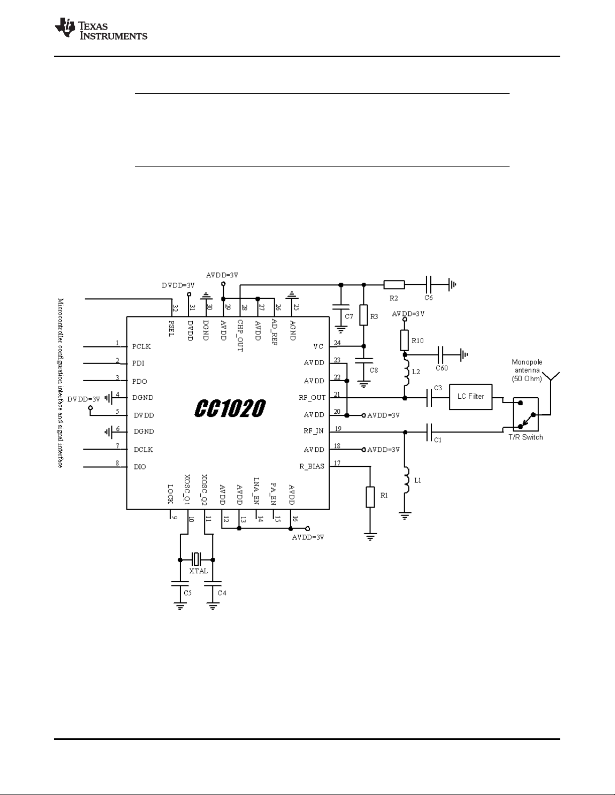
www.ti.com
6 Applications, Implementation, and Layout
Information in Section 6 is not part of the TI component specification, and TI does not
warrant its accuracy or completeness. TI’s customers are responsible for determining
suitability of components for their purposes. Customers should validate and test their design
implementation to confirm system functionality.
6.1 Application Information
Very few external components are required for the operation of CC1020. The recommended application
circuit is shown in Figure 6-1. The external components are described in Table 6-1 and values are given in
Table 6-2.
6.1.1 Typical Application
CC1020
SWRS046H –NOVEMBER 2006–REVISED MARCH 2015
NOTE
Figure 6-1. Typical Application and Test Circuit (Power Supply Decoupling Not Shown)
Copyright © 2006–2015, Texas Instruments Incorporated Applications, Implementation, and Layout 83
Submit Documentation Feedback
Product Folder Links: CC1020
Page 84
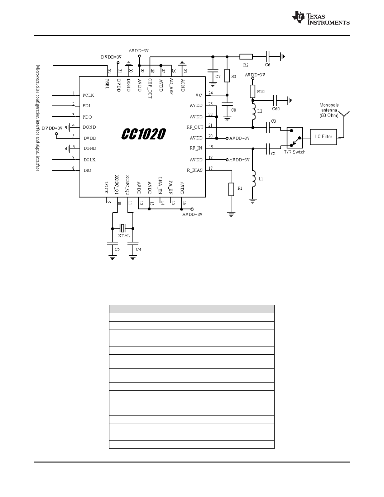
CC1020
SWRS046H –NOVEMBER 2006–REVISED MARCH 2015
www.ti.com
Figure 6-2. Alternative Application Circuit (Power Supply Decoupling Not Shown)
Table 6-1. Overview of External Components
(Excluding Supply Decoupling Capacitors)
REF DESCRIPTION
C1 LNA input match and DC block, see Section 5.11
C3 PA output match and DC block, see Section 5.11
C4 Crystal load capacitor, see Section 5.16
C5 Crystal load capacitor, see Section 5.16
C6 PLL loop filter capacitor
PLL loop filter capacitor (may be omitted for highest loop
C7
bandwidth)
PLL loop filter capacitor (may be omitted for highest loop
C8
bandwidth)
C60 Decoupling capacitor
L1 LNA match and DC bias (ground), see Section 5.11
L2 PA match and DC bias (supply voltage), see Section 5.11
R1 Precision resistor for current reference generator
R2 PLL loop filter resistor
R3 PLL loop filter resistor
R10 PA output match, see Section 5.11
XTAL Crystal, see Section 5.16
84 Applications, Implementation, and Layout Copyright © 2006–2015, Texas Instruments Incorporated
Submit Documentation Feedback
Product Folder Links: CC1020
Page 85

www.ti.com
CC1020
SWRS046H –NOVEMBER 2006–REVISED MARCH 2015
Table 6-2. Bill of Materials for the Application Circuit In Figure 6-1
ITEM 433 MHz 868 MHz 915 MHz
(3)
C1
(3)
C3
C4 22 pF, 5%, NP0, 0402 22 pF, 5%, NP0, 0402 22 pF, 5%, NP0, 0402
C5 12 pF, 5%, NP0, 0402 12 pF, 5%, NP0, 0402 12 pF, 5%, NP0, 0402
C6 220 nF, 10%, X7R, 0603 100 nF, 10%, X7R, 0603 100 nF, 10%, X7R, 0603
C7 8.2 nF, 10%, X7R, 0402 3.9 nF, 10%, X7R, 0402 3.9 nF, 10%, X7R, 0402
C8 2.2 nF, 10%, X7R, 0402 1.0 nF, 10%, X7R, 0402 1.0 nF, 10%, X7R, 0402
C60 220 pF, 5%, NP0, 0402 220 pF, 5%, NP0, 0402 220 pF, 5%, NP0, 0402
(3)
L1
(3)
L2
R1 82 kΩ, 1%, 0402 82 kΩ, 1%, 0402 82 kΩ, 1%, 0402
R2 1.5 kΩ, 5%, 0402 2.2 kΩ, 5%, 0402 2.2 kΩ, 5%, 0402
R3 4.7 kΩ, 5%, 0402 6.8 kΩ, 5%, 0402 6.8 kΩ, 5%, 0402
R10 82 Ω, 5%, 0402 82 Ω, 5%, 0402 82 Ω, 5%, 0402
XTAL
(1) The PLL loop filter component values in Table 6-2 (R2, R3, C6-C8) can be used for data rates up to 4.8 kBaud.
(2) The SmartRF Studio software provides component values for other data rates using the equations in Section 5.12.2.
(3) Items shaded vary for different frequencies. For 433 MHz, 12.5 kHz channel, a loop filter with lower bandwidth is used to improve
adjacent and alternate channel rejection.
10 pF, 5%, NP0, 0402 47 pF, 5%, NP0, 0402 47 pF, 5%, NP0, 0402
5.6 pF, 5%, NP0, 0402 10 pF, 5%, NP0, 0402 10 pF, 5%, NP0, 0402
33 nH, 5%, 0402 82 nH, 5%, 0402 82 nH, 5%, 0402
22 nH, 5%, 0402 3.6 nH, 5%, 0402 3.6 nH, 5%, 0402
14.7456 MHz crystal, 14.7456 MHz crystal, 14.7456 MHz crystal,
16 pF load 16 pF load 16 pF load
(1)(2)
In the CC1020EMX reference design (CC1020EMX), LQG15HS series inductors from Murata have been
used. The switch is SW-456 from M/A-COM.
The LC filter in Figure 6-1 is inserted in the TX path only. The filter will reduce the emission of harmonics
and the spurious emissions in the TX path. An alternative is to insert the LC filter between the antenna
and the T/R switch as shown in Figure 6-2.
The filter will reduce the emission of harmonics and the spurious emissions in the TX path as well as
increase the receiver selectivity. The sensitivity will be slightly reduced due to the insertion loss of the LC
filter.
6.2 Design Requirements
6.2.1 Input and Output Matching
L1 and C1 are the input match for the receiver. L1 is also a DC choke for biasing. L2 and C3 are used to
match the transmitter to 50 Ω. Internal circuitry makes it possible to connect the input and output together
and match the CC1020 to 50 Ω in both RX and TX mode. However, it is recommended to use an external
T/R switch for optimum performance. See Section 5.11 for details. Component values for the matching
network are easily found using the SmartRF Studio software.
6.2.2 Bias Resistor
The precision bias resistor R1 is used to set an accurate bias current.
6.2.3 PLL Loop Filter
The loop filter consists of two resistors (R2 and R3) and three capacitors (C6 through C8). C7 and C8 may
be omitted in applications where high loop bandwidth is desired. The values shown in Table 6-2 can be
used for data rates up to 4.8 kBaud. Component values for higher data rates are easily found using the
SmartRF Studio software.
Copyright © 2006–2015, Texas Instruments Incorporated Applications, Implementation, and Layout 85
Submit Documentation Feedback
Product Folder Links: CC1020
Page 86

CC1020
SWRS046H –NOVEMBER 2006–REVISED MARCH 2015
6.2.4 Crystal
An external crystal with two loading capacitors (C4 and C5) is used for the crystal oscillator. See
Section 5.16 for details.
6.2.5 Additional Filtering
Additional external components (for example, RF, LC, or SAW filter) may be used in order to improve the
performance in specific applications. See Section 5.11 for further information.
6.2.6 Power Supply Decoupling and Filtering
Power supply decoupling and filtering must be used (not shown in the application circuit). The placement
and size of the decoupling capacitors and the power supply filtering are very important to achieve the
optimum performance for narrowband applications. TI provides a reference design that should be followed
very closely.
6.3 PCB Layout Recommendations
The top layer should be used for signal routing, and the open areas should be filled with metallization
connected to ground using several vias.
The area under the chip is used for grounding and must be connected to the bottom ground plane with
several vias. In the TI reference designs we have placed 9 vias inside the exposed die attached pad.
These vias should be “tented” (covered with solder mask) on the component side of the PCB to avoid
migration of solder through the vias during the solder reflow process.
www.ti.com
Do not place a via underneath CC1020 at “pin #1 corner” as this pin is internally connected to the exposed
die attached pad, which is the main ground connection for the chip.
Each decoupling capacitor should be placed as close as possible to the supply pin it is supposed to
decouple. Each decoupling capacitor should be connected to the power line (or power plane) by separate
vias. The best routing is from the power line (or power plane) to the decoupling capacitor and then to the
CC1020 supply pin. Supply power filtering is very important, especially for pins 23, 22, 20 and 18.
Each decoupling capacitor ground pad should be connected to the ground plane using a separate via.
Direct connections between neighboring power pins will increase noise coupling and should be avoided
unless absolutely necessary.
The external components should ideally be as small as possible and surface mount devices are highly
recommended.
Precaution should be used when placing the microcontroller in order to avoid noise interfering with the RF
circuitry.
A CC1020/1070DK Development Kit with a fully assembled CC1020EMX Evaluation Module is available.
It is strongly advised that this reference layout is followed very closely in order to get the best
performance. The layout Gerber files are available from the CC1020EMX product folder.
86 Applications, Implementation, and Layout Copyright © 2006–2015, Texas Instruments Incorporated
Submit Documentation Feedback
Product Folder Links: CC1020
Page 87

www.ti.com
7 Device and Documentation Support
7.1 Device Support
7.1.1 Device Nomenclature
To designate the stages in the product development cycle, TI assigns prefixes to the part numbers. Each
device has one of three prefixes: X, P, or null (no prefix) (for example, CC1020 is in production; therefore,
no prefix is assigned).
Device development evolutionary flow:
X Experimental device that is not necessarily representative of the final device's electrical
specifications and may not use production assembly flow.
P Prototype device that is not necessarily the final silicon die and may not necessarily meet
final electrical specifications.
null Production version of the silicon die that is fully qualified.
Production devices have been characterized fully, and the quality and reliability of the device have been
demonstrated fully. TI's standard warranty applies.
Predictions show that prototype devices (X or P) have a greater failure rate than the standard production
devices. Texas Instruments recommends that these devices not be used in any production system
because their expected end-use failure rate still is undefined. Only qualified production devices are to be
used.
CC1020
SWRS046H –NOVEMBER 2006–REVISED MARCH 2015
TI device nomenclature also includes a suffix with the device family name. This suffix indicates the
package type (for example, RSS).
For orderable part numbers of CC1020 devices in the RSS package types, see the Package Option
Addendum of this document, the TI website (www.ti.com), or contact your TI sales representative.
7.2 Documentation Support
The following documents describe the CC1020 device. Copies of these documents are available on the
Internet at www.ti.com.
1. [1] AN022 CC1020 Crystal Frequency Selection (SWRA070)
2. [2] AN029 CC1020/1021 Automatic Frequency Control (AFC) (SWRA063)
3. [3] AN030 CC1020/1021 Received Signal Strength Indicator (SWRA062)
4. [4] AN070 CC1020 Automatic Power-Up Sequencing (SWRA279)
5. [5] AN023 CC1020 MCU Interfacing (SWRA069)
6. [6] CC1020 Errata Note 004, available in the CC1020 product folder.
7. [7] CC1020 Errata Note 002, available in the CC1020 product folder.
8. [8] AN001 SRD Regulations For License Free Transceiver Operation (SWRA090).
9. [9] AN027 Temperature Compensation by Indirect Method (SWRA065)
10. [10] AN003 SRD Antennas (SWRA088)
11. [11] SmartRF Studio
12. [12] CC1020EMX Evaluation Module
7.2.1 Community Resources
The following links connect to TI community resources. Linked contents are provided "AS IS" by the
respective contributors. They do not constitute TI specifications and do not necessarily reflect TI's views;
see TI's Terms of Use.
TI E2E™ Online Community TI's Engineer-to-Engineer (E2E) Community. Created to foster
Copyright © 2006–2015, Texas Instruments Incorporated Device and Documentation Support 87
Submit Documentation Feedback
Product Folder Links: CC1020
Page 88
CC1020
SWRS046H –NOVEMBER 2006–REVISED MARCH 2015
collaboration among engineers. At e2e.ti.com, you can ask questions, share knowledge,
explore ideas and help solve problems with fellow engineers.
TI Embedded Processors Wiki Texas Instruments Embedded Processors Wiki. Established to help
developers get started with Embedded Processors from Texas Instruments and to foster
innovation and growth of general knowledge about the hardware and software surrounding
these devices.
7.3 Trademarks
SmartRF, E2E are trademarks of Texas Instruments.
7.4 Electrostatic Discharge Caution
This integrated circuit can be damaged by ESD. Texas Instruments recommends that all integrated circuits be handled with
appropriate precautions. Failure to observe proper handling and installation procedures can cause damage.
ESD damage can range from subtle performance degradation to complete device failure. Precision integrated circuits may be more
susceptible to damage because very small parametric changes could cause the device not to meet its published specifications.
7.5 Export Control Notice
Recipient agrees to not knowingly export or re-export, directly or indirectly, any product or technical data
(as defined by the U.S., EU, and other Export Administration Regulations) including software, or any
controlled product restricted by other applicable national regulations, received from disclosing party under
nondisclosure obligations (if any), or any direct product of such technology, to any destination to which
such export or re-export is restricted or prohibited by U.S. or other applicable laws, without obtaining prior
authorization from U.S. Department of Commerce and other competent Government authorities to the
extent required by those laws.
www.ti.com
7.6 Glossary
SLYZ022 — TI Glossary.
This glossary lists and explains terms, acronyms, and definitions.
8 Mechanical Packaging and Orderable Information
8.1 Packaging Information
The following pages include mechanical packaging and orderable information. This information is the most
current data available for the designated devices. This data is subject to change without notice and
revision of this document. For browser-based versions of this data sheet, refer to the left-hand navigation.
88 Mechanical Packaging and Orderable Information Copyright © 2006–2015, Texas Instruments Incorporated
Submit Documentation Feedback
Product Folder Links: CC1020
Page 89
PACKAGE OPTION ADDENDUM
www.ti.com
PACKAGING INFORMATION
Orderable Device Status
CC1020-RTB1 OBSOLETE VQFNP RUZ 32 TBD Call TI Call TI -40 to 85 CC1020
CC1020-RTR1 NRND VQFNP RUZ 32 Green (RoHS
CC1020RSS OBSOLETE VQFNP RUZ 32 TBD Call TI Call TI -40 to 85 CC1020
CC1020RSSG4 ACTIVE QFN RSS 32 TBD Call TI Call TI -40 to 85
CC1020RSSR ACTIVE QFN RSS 32 2500 Green (RoHS
CC1020RSST ACTIVE QFN RSS 32 250 Green (RoHS
CC1020RUZ OBSOLETE VQFNP RUZ 32 TBD Call TI Call TI -40 to 85 CC1020
CC1020RUZR OBSOLETE VQFNP RUZ 32 Green (RoHS
(1)
The marketing status values are defined as follows:
ACTIVE: Product device recommended for new designs.
LIFEBUY: TI has announced that the device will be discontinued, and a lifetime-buy period is in effect.
NRND: Not recommended for new designs. Device is in production to support existing customers, but TI does not recommend using this part in a new design.
PREVIEW: Device has been announced but is not in production. Samples may or may not be available.
OBSOLETE: TI has discontinued the production of the device.
Package Type Package
(1)
Drawing
Pins Package
Qty
Eco Plan
(2)
& no Sb/Br)
& no Sb/Br)
& no Sb/Br)
& no Sb/Br)
Lead/Ball Finish
(6)
CU NIPDAU Level-3-260C-168 HR -40 to 85 CC1020
CU NIPDAU Level-3-260C-168 HR -40 to 85 CC1020
CU NIPDAU Level-3-260C-168 HR -40 to 85 CC1020
CU NIPDAU Level-3-260C-168 HR -40 to 85 CC1020
MSL Peak Temp
(3)
Op Temp (°C) Device Marking
(4/5)
(2)
Eco Plan - The planned eco-friendly classification: Pb-Free (RoHS), Pb-Free (RoHS Exempt), or Green (RoHS & no Sb/Br) - please check http://www.ti.com/productcontent for the latest availability
information and additional product content details.
TBD: The Pb-Free/Green conversion plan has not been defined.
Pb-Free (RoHS): TI's terms "Lead-Free" or "Pb-Free" mean semiconductor products that are compatible with the current RoHS requirements for all 6 substances, including the requirement that
lead not exceed 0.1% by weight in homogeneous materials. Where designed to be soldered at high temperatures, TI Pb-Free products are suitable for use in specified lead-free processes.
Pb-Free (RoHS Exempt): This component has a RoHS exemption for either 1) lead-based flip-chip solder bumps used between the die and package, or 2) lead-based die adhesive used between
the die and leadframe. The component is otherwise considered Pb-Free (RoHS compatible) as defined above.
Green (RoHS & no Sb/Br): TI defines "Green" to mean Pb-Free (RoHS compatible), and free of Bromine (Br) and Antimony (Sb) based flame retardants (Br or Sb do not exceed 0.1% by weight
in homogeneous material)
(3)
MSL, Peak Temp. - The Moisture Sensitivity Level rating according to the JEDEC industry standard classifications, and peak solder temperature.
(4)
There may be additional marking, which relates to the logo, the lot trace code information, or the environmental category on the device.
7-Mar-2016
Samples
Addendum-Page 1
Page 90
PACKAGE OPTION ADDENDUM
www.ti.com
(5)
Multiple Device Markings will be inside parentheses. Only one Device Marking contained in parentheses and separated by a "~" will appear on a device. If a line is indented then it is a continuation
of the previous line and the two combined represent the entire Device Marking for that device.
(6)
Lead/Ball Finish - Orderable Devices may have multiple material finish options. Finish options are separated by a vertical ruled line. Lead/Ball Finish values may wrap to two lines if the finish
value exceeds the maximum column width.
Important Information and Disclaimer:The information provided on this page represents TI's knowledge and belief as of the date that it is provided. TI bases its knowledge and belief on information
provided by third parties, and makes no representation or warranty as to the accuracy of such information. Efforts are underway to better integrate information from third parties. TI has taken and
continues to take reasonable steps to provide representative and accurate information but may not have conducted destructive testing or chemical analysis on incoming materials and chemicals.
TI and TI suppliers consider certain information to be proprietary, and thus CAS numbers and other limited information may not be available for release.
In no event shall TI's liability arising out of such information exceed the total purchase price of the TI part(s) at issue in this document sold by TI to Customer on an annual basis.
7-Mar-2016
Addendum-Page 2
Page 91
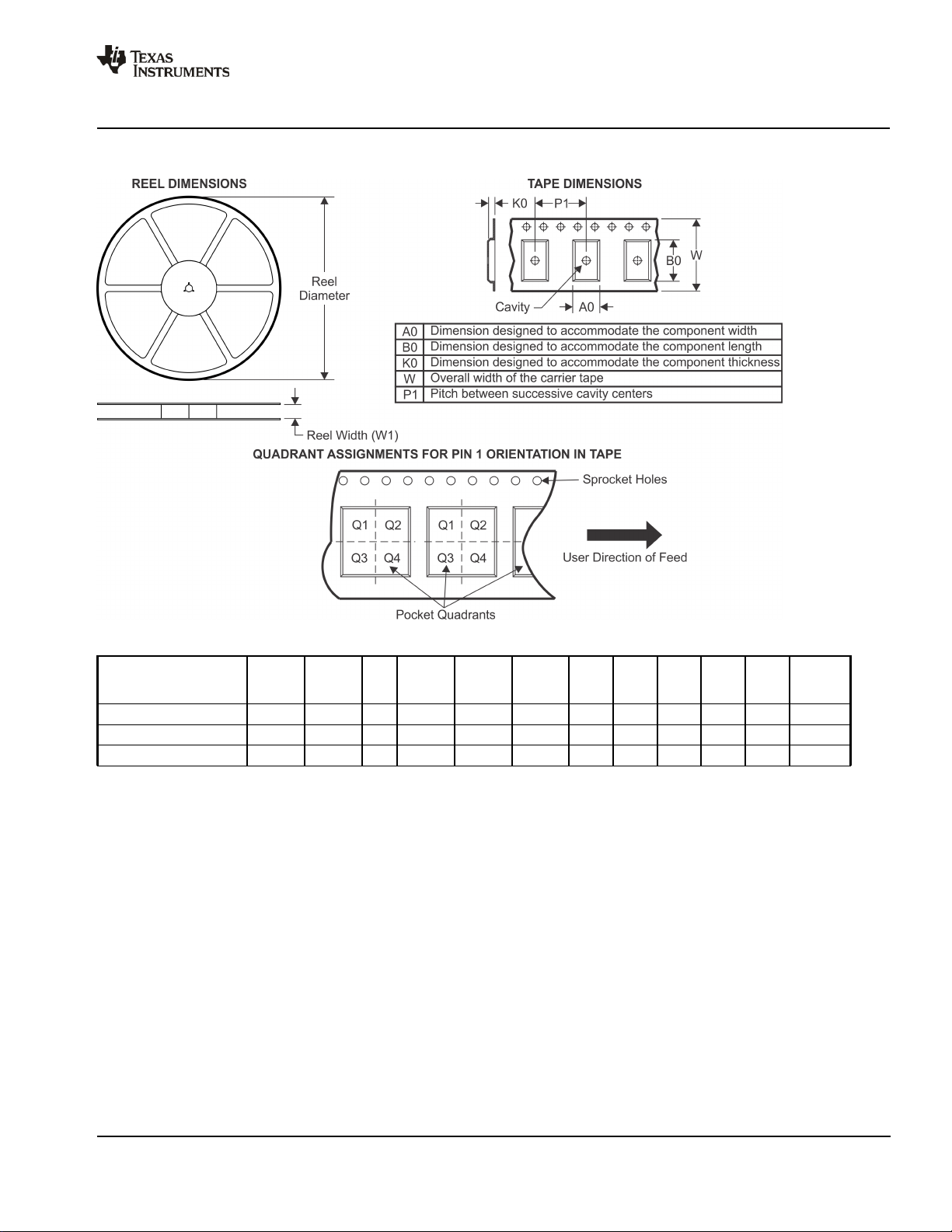
PACKAGE MATERIALS INFORMATION
www.ti.com 21-Nov-2016
TAPE AND REEL INFORMATION
*All dimensions are nominal
Device Package
CC1020RSSR QFN RSS 32 2500 330.0 16.4 7.3 7.3 1.5 12.0 16.0 Q2
CC1020RSST QFN RSS 32 250 180.0 16.4 7.3 7.3 1.5 12.0 16.0 Q2
CC1020RUZR VQFNP RUZ 32 0 330.0 16.4 7.3 7.3 1.5 12.0 16.0 Q2
Type
Package
Drawing
Pins SPQ Reel
Diameter
(mm)
Reel
Width
W1 (mm)
A0
(mm)B0(mm)K0(mm)P1(mm)W(mm)
Pin1
Quadrant
Pack Materials-Page 1
Page 92
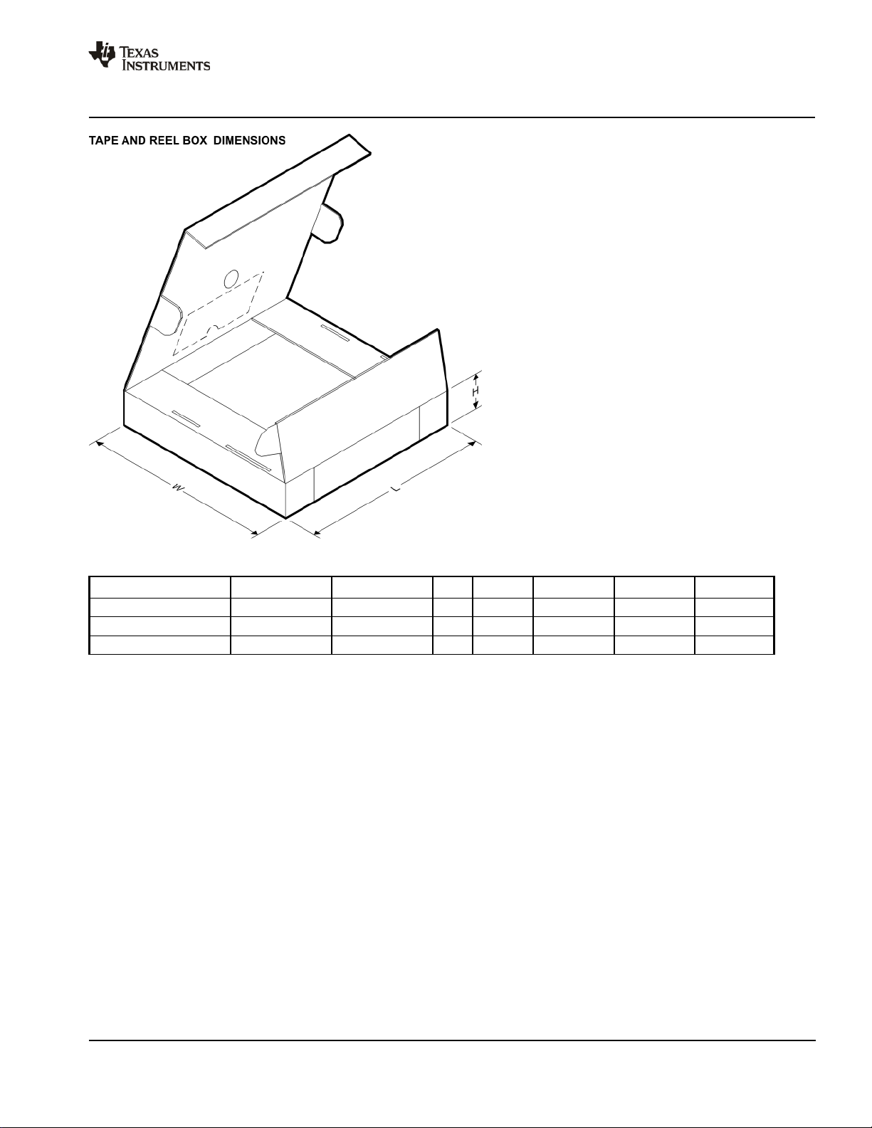
PACKAGE MATERIALS INFORMATION
www.ti.com 21-Nov-2016
*All dimensions are nominal
Device Package Type Package Drawing Pins SPQ Length (mm) Width (mm) Height (mm)
CC1020RSSR QFN RSS 32 2500 336.6 336.6 28.6
CC1020RSST QFN RSS 32 250 213.0 191.0 55.0
CC1020RUZR VQFNP RUZ 32 0 336.6 336.6 28.6
Pack Materials-Page 2
Page 93
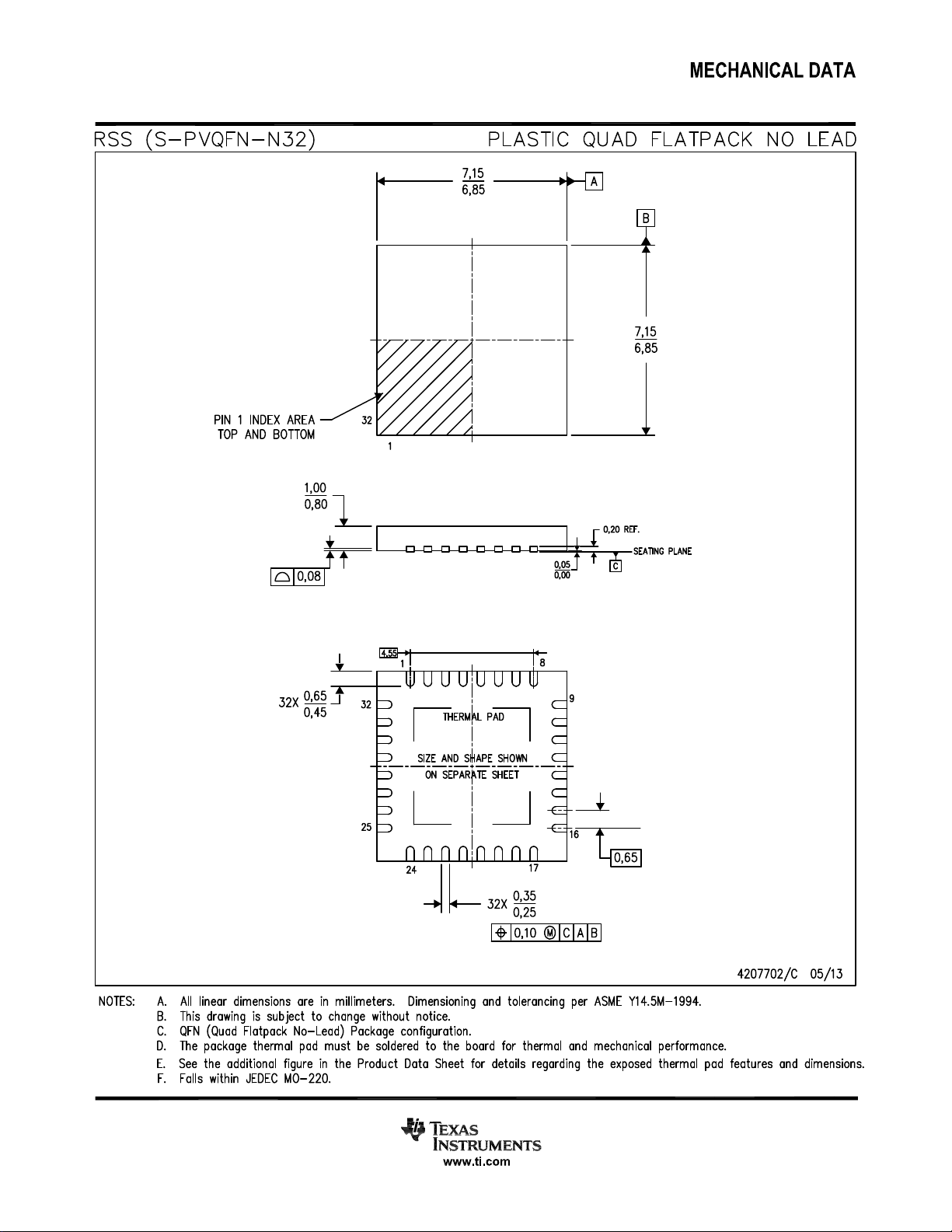
Page 94
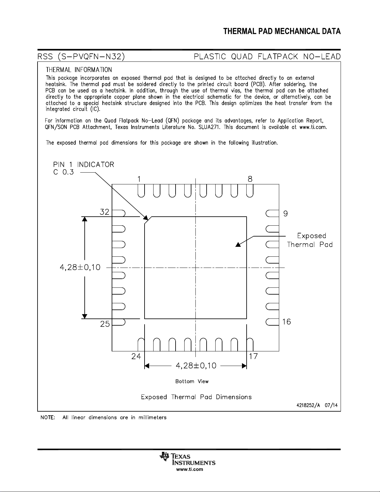
Page 95

IMPORTANT NOTICE
Texas Instruments Incorporated and its subsidiaries (TI) reserve the right to make corrections, enhancements, improvements and other
changes to its semiconductor products and services per JESD46, latest issue, and to discontinue any product or service per JESD48, latest
issue. Buyers should obtain the latest relevant information before placing orders and should verify that such information is current and
complete. All semiconductor products (also referred to herein as “components”) are sold subject to TI’s terms and conditions of sale
supplied at the time of order acknowledgment.
TI warrants performance of its components to the specifications applicable at the time of sale, in accordance with the warranty in TI’s terms
and conditions of sale of semiconductor products. Testing and other quality control techniques are used to the extent TI deems necessary
to support this warranty. Except where mandated by applicable law, testing of all parameters of each component is not necessarily
performed.
TI assumes no liability for applications assistance or the design of Buyers’ products. Buyers are responsible for their products and
applications using TI components. To minimize the risks associated with Buyers’ products and applications, Buyers should provide
adequate design and operating safeguards.
TI does not warrant or represent that any license, either express or implied, is granted under any patent right, copyright, mask work right, or
other intellectual property right relating to any combination, machine, or process in which TI components or services are used. Information
published by TI regarding third-party products or services does not constitute a license to use such products or services or a warranty or
endorsement thereof. Use of such information may require a license from a third party under the patents or other intellectual property of the
third party, or a license from TI under the patents or other intellectual property of TI.
Reproduction of significant portions of TI information in TI data books or data sheets is permissible only if reproduction is without alteration
and is accompanied by all associated warranties, conditions, limitations, and notices. TI is not responsible or liable for such altered
documentation. Information of third parties may be subject to additional restrictions.
Resale of TI components or services with statements different from or beyond the parameters stated by TI for that component or service
voids all express and any implied warranties for the associated TI component or service and is an unfair and deceptive business practice.
TI is not responsible or liable for any such statements.
Buyer acknowledges and agrees that it is solely responsible for compliance with all legal, regulatory and safety-related requirements
concerning its products, and any use of TI components in its applications, notwithstanding any applications-related information or support
that may be provided by TI. Buyer represents and agrees that it has all the necessary expertise to create and implement safeguards which
anticipate dangerous consequences of failures, monitor failures and their consequences, lessen the likelihood of failures that might cause
harm and take appropriate remedial actions. Buyer will fully indemnify TI and its representatives against any damages arising out of the use
of any TI components in safety-critical applications.
In some cases, TI components may be promoted specifically to facilitate safety-related applications. With such components, TI’s goal is to
help enable customers to design and create their own end-product solutions that meet applicable functional safety standards and
requirements. Nonetheless, such components are subject to these terms.
No TI components are authorized for use in FDA Class III (or similar life-critical medical equipment) unless authorized officers of the parties
have executed a special agreement specifically governing such use.
Only those TI components which TI has specifically designated as military grade or “enhanced plastic” are designed and intended for use in
military/aerospace applications or environments. Buyer acknowledges and agrees that any military or aerospace use of TI components
which have not been so designated is solely at the Buyer's risk, and that Buyer is solely responsible for compliance with all legal and
regulatory requirements in connection with such use.
TI has specifically designated certain components as meeting ISO/TS16949 requirements, mainly for automotive use. In any case of use of
non-designated products, TI will not be responsible for any failure to meet ISO/TS16949.
Products Applications
Audio www.ti.com/audio Automotive and Transportation www.ti.com/automotive
Amplifiers amplifier.ti.com Communications and Telecom www.ti.com/communications
Data Converters dataconverter.ti.com Computers and Peripherals www.ti.com/computers
DLP® Products www.dlp.com Consumer Electronics www.ti.com/consumer-apps
DSP dsp.ti.com Energy and Lighting www.ti.com/energy
Clocks and Timers www.ti.com/clocks Industrial www.ti.com/industrial
Interface interface.ti.com Medical www.ti.com/medical
Logic logic.ti.com Security www.ti.com/security
Power Mgmt power.ti.com Space, Avionics and Defense www.ti.com/space-avionics-defense
Microcontrollers microcontroller.ti.com Video and Imaging www.ti.com/video
RFID www.ti-rfid.com
OMAP Applications Processors www.ti.com/omap TI E2E Community e2e.ti.com
Wireless Connectivity www.ti.com/wirelessconnectivity
Mailing Address: Texas Instruments, Post Office Box 655303, Dallas, Texas 75265
Copyright © 2016, Texas Instruments Incorporated
 Loading...