

Page 1
CA3039
November 1996
Features
• Six Matched Diodes on a Common Substrate
• Excellent Reverse Recovery Time . . . . . . . . . 1ns (Typ)
Match . . . . . . . . . . . . . . . . . . . . . . . . . . . . 5mV (Max)
•V
F
• Low Capacitance . . . . . . C
= 0.65pF (Typ) at VR = -2V
D
Applications
• Ultra-Fast Low Capacitance Matched Diodes for
Applications in Communications and Switching
Systems
• Balanced Modulators or Demodulators
• Ring Modulators
• High Speed Diode Gates
• Analog Switches
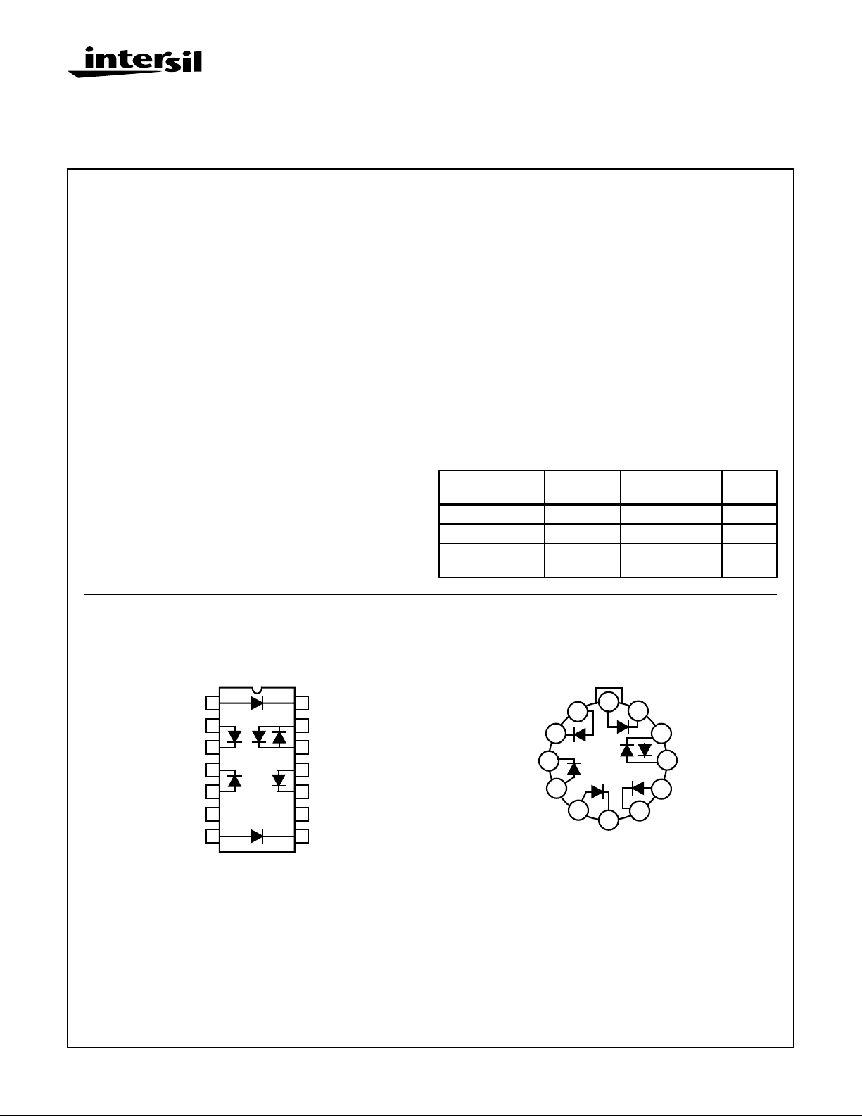
Diode Array
Description
The CA3039 consists of six ultra-fast, low capacitance
diodes on a common monolithic substrate. Integrated circuit
construction assures excellent static and dynamic matching
of the diodes, making the array extremely useful for a wide
variety of applications in communication and switching
systems.
Five of the diodes are independently accessible, the sixth
shares a common terminal with the substrate.
For applications such as balanced modulators or ring
modulators where capacitive balance is important, the
substrate should be returned to a DC potential which is
significantly more negative (with respect to the active diodes)
than the peak signal applied.
Ordering Information
TEMP.
PART NUMBER
CA3039 -55 to 125 12 Pin Metal Can T12.B
CA3039M -55 to 125 14 Ld SOIC M14.15
CA3039M96 -55 to 125 14 Ld SOIC Tape
RANGE (oC) PACKAGE
and Reel
PKG.
NO.
M14.15
Pinouts
NC
CA3039
(SOIC)
TOP VIEW
1
2
3
D
4
4
5
D
3
6
7
CA3039
(METAL CAN)
TOP VIEW
D
D
14
5
13
SUBSTRATE
12
D
6DS
11
10
D
1
NC
9
2
8
2
3
4
12
1
D
4
D
3
D
5
11
D
5
D
2
6
10
6
D
9
D
S
1
8
7
CAUTION: These devices are sensitive to electrostatic discharge; follow proper IC Handling Procedures.
1-888-INTERSIL or 321-724-7143
| Copyright © Intersil Corporation 1999
7-18
File Number 343.3
Page 2
CA3039
Absolute Maximum Ratings Thermal Information
Inverse Voltage (PIV) for: D1 - D5 . . . . . . . . . . . . . . . . . . . . . . . . 5V
D6. . . . . . . . . . . . . . . . . . . . . . .0.5V
Diode-to-Substrate Voltage (VDI) for D1 - D5. . . . . . . . . . . .20V, -1V
(Terminal 1, 4, 5, 8 or 12 to Terminal 10)
DC Forward Current (IF). . . . . . . . . . . . . . . . . . . . . . . . . . . . . .25mA
Recurrent Forward Current (IF) . . . . . . . . . . . . . . . . . . . . . . .100mA
Forward Surge Current (I
(SURGE)
F
). . . . . . . . . . . . . . . . . . . .100mA
Operating Conditions
Temperature Range . . . . . . . . . . . . . . . . . . . . . . . . -55oC to 125oC
CAUTION: Stresses above those listed in “Absolute Maximum Ratings” may cause permanent damage to the device. This is a stress only rating and operation
of the device at these or any other conditions above those indicated in the operational sections of this specification is not implied.
NOTE:
1. θJA is measured with the component mounted on an evaluation PC board in free air.
Thermal Resistance (Typical, Note 1) θJA (oC/W) θJC (oC/W)
Metal Can Package. . . . . . . . . . . . . . . 200 120
SOIC Package. . . . . . . . . . . . . . . . . . . 220 N/A
Maximum Power Dissipation (Any One Diode) . . . . . . . . . . .100mW
Maximum Junction Temperature (Metal Can Package) . . . . . . . 175oC
Maximum Junction Temperature (Plastic Package) . . . . . . . . 150oC
Maximum Storage Temperature Range . . . . . . . . . -65oC to 150oC
Maximum Lead Temperature (Soldering 10s) . . . . . . . . . . . . 300oC
(SOIC - Lead Tips Only)
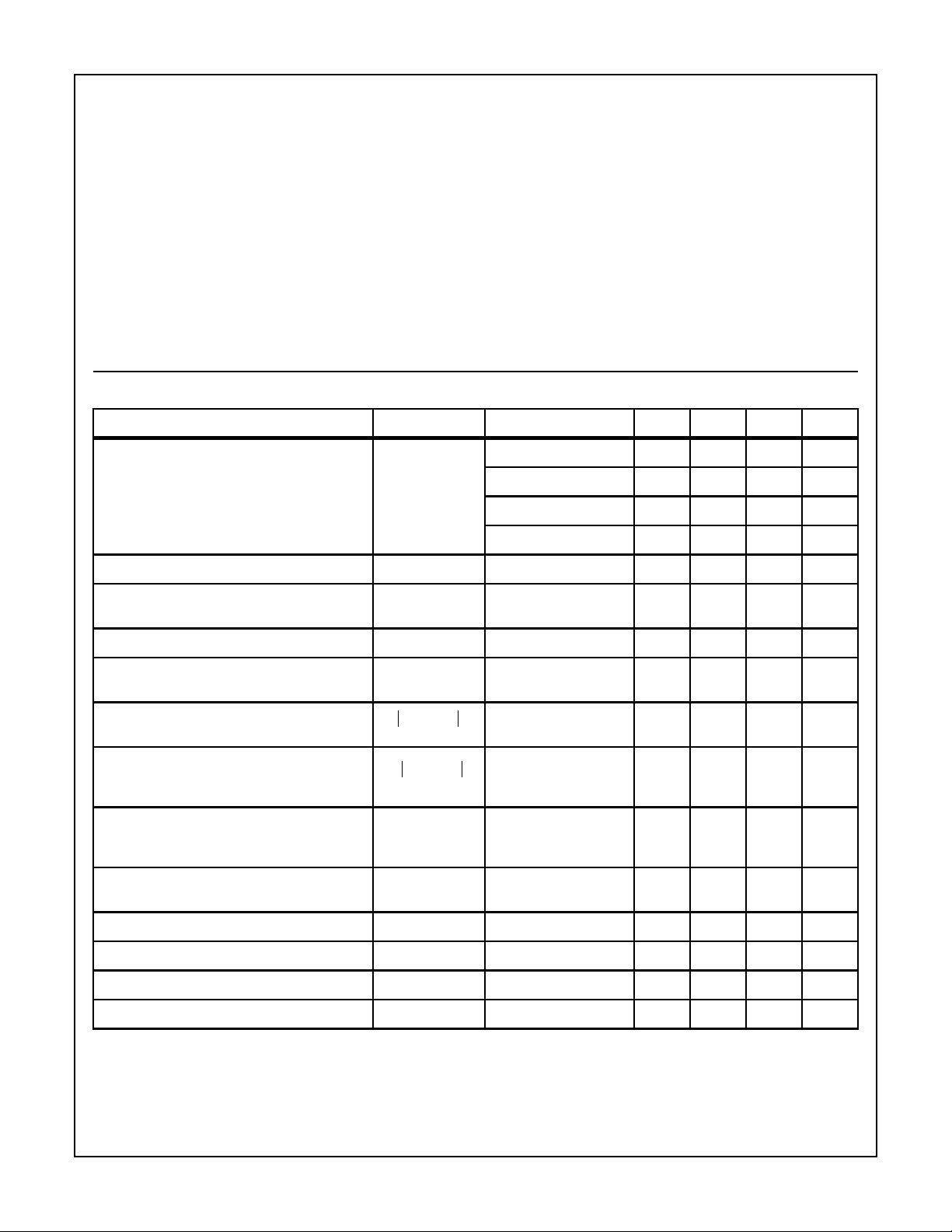
Electrical Specifications T
= 25oC; Characteristics apply for each diode unit, Unless Otherwise Specified
A
PARAMETER SYMBOL TEST CONDITIONS MIN TYP MAX UNITS
DC Forward Voltage Drop (Figure 1) V
DC Reverse Breakdown Voltage V
DC Reverse Breakdown Voltage Between Any
Diode Unit and Substrate
DC Reverse (Leakage) Current (Figure 2) I
DC Reverse (Leakage) Current Between Any
Diode Unit and Substrate (Figure 3)
Magnitude of Diode Offset Voltage (Note 2)
VF1VF2–
(Figure 1)
Temperature Coefficient of |V
- VF2| (Figure 4) IF = 1mA - 1.0 - µV/oC
F1
∆ VF1VF2–
----------------------------------
Temperature Coefficient of Forward Drop
(Figure 5)
(BR)R
V
(BR)R
∆T
∆V
-----------
∆T
F
IF = 50µA - 0.65 0.69 V
= 1mA - 0.73 0.78 V
I
F
I
= 3mA - 0.76 0.80 V
F
= 10mA - 0.81 0.90 V
I
F
IR = -10µA57-V
IR = -10µA20--V
R
I
R
F
VR = -4V - 0.016 100 nA
VR = -10V - 0.022 100 nA
I
= 1mA - 0.5 5.0 mV
F
= 1mA - -1.9 - mV/oC
I
F
DC Forward Voltage Drop for Anode-toSubstrate Diode (D
)
S
Reverse Recovery Time t
Diode Resistance (Figure 6) R
Diode Capacitance (Figure 7) C
Diode-to-Substrate Capacitance (Figure 8) C
V
RR
F
D
D
DI
IF = 1mA - 0.65 - V
IF = 10mA, IR = -10mA - 1.0 - ns
f = 1kHz, IF = 1mA 25 30 45 Ω
VR = -2V, IF = 0 - 0.65 - pF
VDI = 4V, IF = 0 - 3.2 - pF
NOTE:
2. Magnitude of Diode Offset Voltage is the difference in DC Forward Voltage Drops of any two diode units.
7-19
Page 3

Typical Performance Curves
TA = 25oC
0.8
CA3039
6
10
VR = -4V
FORWARD VOLTAGE DROP (V
0.7
0.6
DC FORWARD VOLTAGE (V)
0.5
DIODE OFFSET
0.01 0.1 1 10
DC FORWARD CURRENT (mA)
VF1V
)
F
–()
F2
5
4
3
2
1
0
FIGURE 1. DC FORWARD VOLTAGE DROP (ANY DIODE) AND
DIODE OFFSET VOLTAGE vs DC FORWARD
CURRENT
100
VR = -10V
10
1
0.1
0.01
DC REVERSE CURRENT (nA)
1
0.1
0.01
DC REVERSE CURRENT (nA)
DIODE OFFSET VOLTAGE (mV)
0.001
-75
-50 -25 0 25 50 75 100 125
TEMPERATURE (
o
C)
FIGURE 2. DC REVERSE (LEAKAGE) CURRENT (D1 - D5) vs
TEMPERATURE
4
(mV)
3
F2
V
–()
2
F1
V
0.7
0.6
0.5
0.4
IF = 10mA
IF = 1mA
IF = 0.1mA
0.001
-75
-50 -25 0 25 50 75 100 125
TEMPERATURE (
o
C)
FIGURE 3. DC REVERSE (LEAKAGE) CURRENT BETWEEN D1,
D2, D3, D4, D5 AND SUBSTRA TE vsTEMPERATURE
IF = 1mA
0.9
0.8
0.7
0.6
0.5
DC FORWARD VOLTAGE (V)
0.4
-75 -50 -25 0 25 50 75 100 125
TEMPERATURE (
o
C)
FIGURE 5. DC FORWARD VOLTAGE DROP (ANY DIODE) vs
TEMPERATURE
0.3
DIODE OFFSET VOLTAGE
-75 -50 -25 0 25 50 75 100 125
TEMPERATURE (
o
C)
FIGURE 4. DIODE OFFSET VOLTAGE (ANY DIODE) vs
TEMPERATURE
1000
100
10
DIODE RESISTANCE (Ω)
1
0.01 0.1 1 10
DC FORWARD CURRENT (mA)
TA = 25oC
f = 1kHz
FIGURE 6. DIODE RESIST ANCE (ANY DIODE) vs DC
FORWARD CURRENT
7-20
Page 4

Typical Performance Curves (Continued)
CA3039
6
TA = 25oC
= 0
I
F
5
4
3
2
DIODE CAPACITANCE (pF)
1
01234
DC REVERSE VOLTAGE ACROSS DIODE (V)
FIGURE 7. DIODE CAP ACITANCE (D1 - D5) vs REVERSE
VOLTAGE
6
TA = 25oC
= 0
I
F
5
4
3
2
1
0
DIODE TO SUBSTRATE CAPACITANCE (pF)
01234
DC REVERSE VOLTAGE BETWEEN TERMINALS 1, 4, 5, 8, OR 12
AND SUBSTRATE (TERMINAL 10) (V)
FIGURE 8. DIODE-TO-SUBSTRA TE CAPACIT ANCE vs
REVERSE VOLTAGE
All Intersil semiconductor products are manufactured, assembled and tested under ISO9000 quality systems certification.
Intersil semiconductor products are sold by description only. Intersil Corporation reserves the right to make changes in circuit design and/or specifications at any time without notice. Accordingly, the reader is cautioned to verify that data sheets are current before placing orders. Information furnished by Intersil is believed to be accurate and
reliable. However, no responsibility is assumed by Intersil or its subsidiaries for its use; nor for any infringements of patents or other rights of third parties which may result
from its use. No license is granted by implication or otherwise under any patent or patent rights of Intersil or its subsidiaries.
For information regarding Intersil Corporation and its products, see web site www.intersil.com
Sales Office Headquarters
NORTH AMERICA
Intersil Corporation
P. O. Box 883, Mail Stop 53-204
Melbourne, FL 32902
TEL: (321) 724-7000
FAX: (321) 724-7240
EUROPE
Intersil SA
Mercure Center
100, Rue de la Fusee
1130 Brussels, Belgium
TEL: (32) 2.724.2111
FAX: (32) 2.724.22.05
7-21
ASIA
Intersil (Taiwan) Ltd.
7F-6, No. 101 Fu Hsing North Road
Taipei, Taiwan
Republic of China
TEL: (886) 2 2716 9310
FAX: (886) 2 2715 3029
 Loading...