

Page 1
SOFT RECOVERY
VERY HIGH VOLT AGE
SMALL RECOVERY CHARGE
BYT 11-600 →1000
FAST RECOVERY RECTIFIER DIODES
APPLICATIONS
ANTISATURATION DIODES FOR TRANSIS-
F 126
(Plastic)
TOR BASE DRIVE
SNUBBER DIODES
ABSOL UT E RATINGS (limiting values)
Symbol Parameter Value Unit
I
FRM
I
F (AV)
I
FSM
P
tot
T
stg
T
T
L
Symbol Parameter
Repetive Peak Forward Current
Average Forward Current * T
Surge non Repetitive Forward Current tp = 10ms
Power Dissipation *
Storage and Junction Temperature Range - 55 to + 150
j
Maximum Lead Temperature for Soldering during 10s at 4mm
from Case
≤ 20µs
t
p
75°C
a =
δ = 0.5
Sinusoidal
55°C
T
a =
BYT 11-
600 800 1000
20 A
1A
35 A
1.25 W
- 55 to + 150
230
°C
°C
Unit
V
RRM
Repetitive Peak Reverse Voltage 600 800 1000 V
THERMAL RESISTANCE
Symbol Parameter Value Unit
R
th (j - a)
* On infinite heatsink with 10mm lead length.
November 1994
Junction-ambient* 60
°C/W
1/4
Page 2
BYT11-600 → 1000
ELECTRICAL CHARACTERISTICS
STATIC CHARACTERISTICS
Synbol Test Conditions Min. Typ. Max. Unit
I
R
V
F
Tj = 25°C
Tj = 25°C
V
= V
R
RRM
I
= 1A 1.3 V
F
20
RECOVERY CHARACTERISTICS
Symbol Test Conditions Min. Typ. Max. Unit
t
rr
Tj = 25°C IF = 0.5A IR = 1A I
= 0.25A
rr
100 ns
To evaluate the conduction losses use the following equations:
V
= 1.1 + 0.075 IF P = 1.1 x I
F
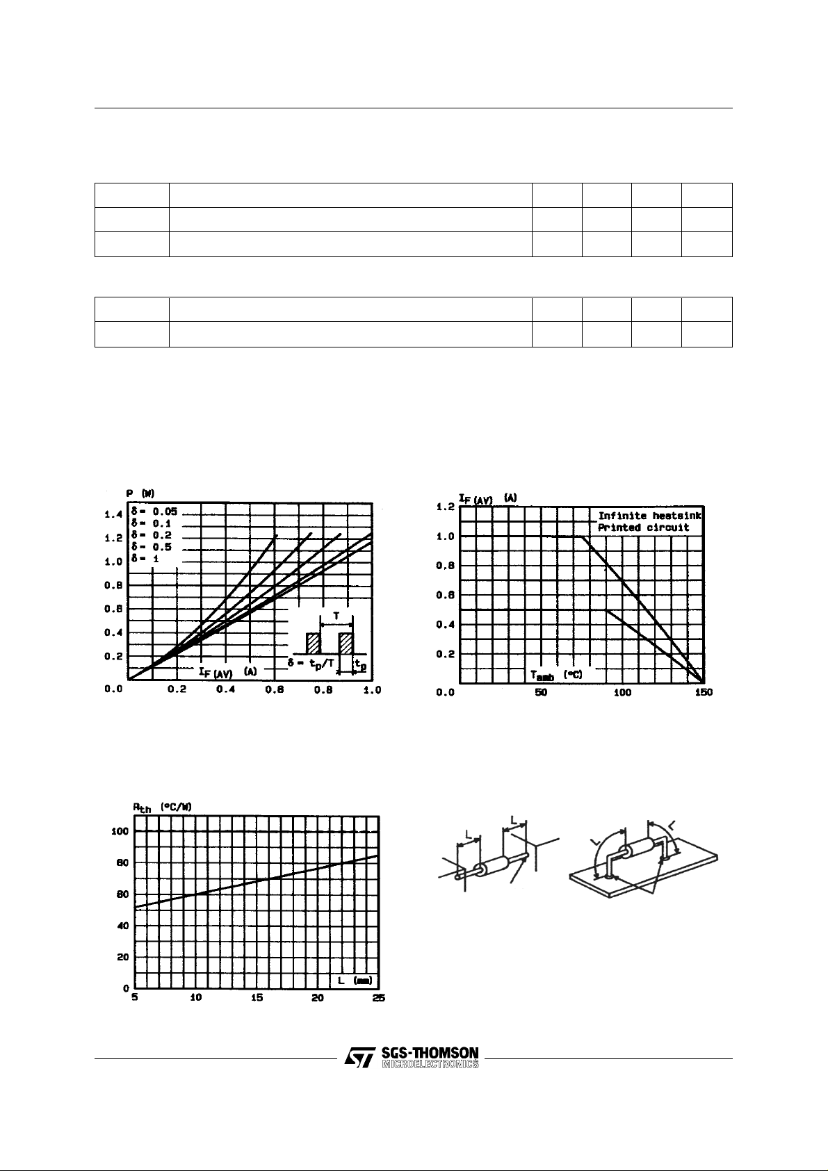
Figure 1. Maximum average power
dissipation versus average forward curr ent .
F(AV)
+ 0.075 I
F2(RMS)
Figure 2. Average forward current versus
ambient temperature.
µA
Figure 3. Thermal resistance versus lead
length.
2/4
Moun ting n°1
INFINIT E HE ATSIN K
Test point of
t
lead
Moun ting n°2
PRINTED CIRCUIT
Soldering
Page 3

Figure 4. Transient thermal impedance
junction-ambient for mounting n°2 versus
pulse duration (L = 10 mm) .
BYT 11-600 → 1000
Figure 5. Peak forward current
versus peak forward voltage drop
(maximum values).
Figure 6. Capacitance versus reverse applied
voltage
Figure 7. Non repetitive surge peak current
versus number of cycles
3/4
Page 4

BYT11-600 → 1000
PACKAGE MECHANICAL DATA
F 126 (Plastic)
DIMENSIONS
REF.
Millimeters Inches
Min. Max. Min. Max.
A 6.05 6.35 0.238 0.250
B 26 1.024
∅ C
∅ D
2.95 3.05 0.116 0.120
0.76 0.86 0.029 0.034
E 1.27 0.050
Cooling method: by convection (method A)
Marking: type number ring at cathode end
Weight: 0.4g
BA B
note 1
E
/
O
D
note 2
E
note 1
O
/
D
NOTES
1 - The lead diameter ∅ D is not controlled over zone E
2 - The minimum axia l lengh within which the device may be
placed with its leads bent at right angles is 0.59"(15 mm)
/
O
C
Information furnished is b elieved to be accurate and reliable. However, SGS-THOMSON Microelectronics assumes no responsability for the
consequences of use of such information nor for any infringement of patents or other rights of third parties which may result from its use. No
license is granted by implication or otherwise under any patent o r patent rights of SGS-THOMSON Microelectronics. Specif ications mentioned
in this publication are subject to change without notice. This publication supersedes an d replaces all information previously supplied.
SGS-THOMSON Microelect ronics product s are not auth orized for use as critical components in life su pport devic es or s ystems wi thout express
written approval of SGS-THOMSON Microelectronics.
© 1994 SGS-THOMSON Microelectronics - Printed in Italy - All rights reserved.
SGS-THOMSON Microelectronics GROUP OF COMPANIES
Australia - Brazil - France - Germany - Hong Kong - Italy - Japan - Korea - Malaysia - Malta - Morocco - The Netherlands -
Singapore - Spain - Sweden - Switzerland - Taiwan - United Kingdom - U.S.A.
4/4
 Loading...