

Page 1
®
FAST RECOV ERY REC T IFI ER DIO D E
MAJOR PRODUC TS CHARACTERISTICS
BYT03-400
I
F(AV)
V
RRM
t
rr
(max) 1.4 V
V
F
3 A
400 V
25 ns
FEATURES
VERY LOW REVERS E RECOVERY TIME
VERY LOW SWITCHING LOSSES
LOW NOISE TURN-OFF SWITCHING
DESCR IPTIO N
Free wheeling diode in converters and motor con-
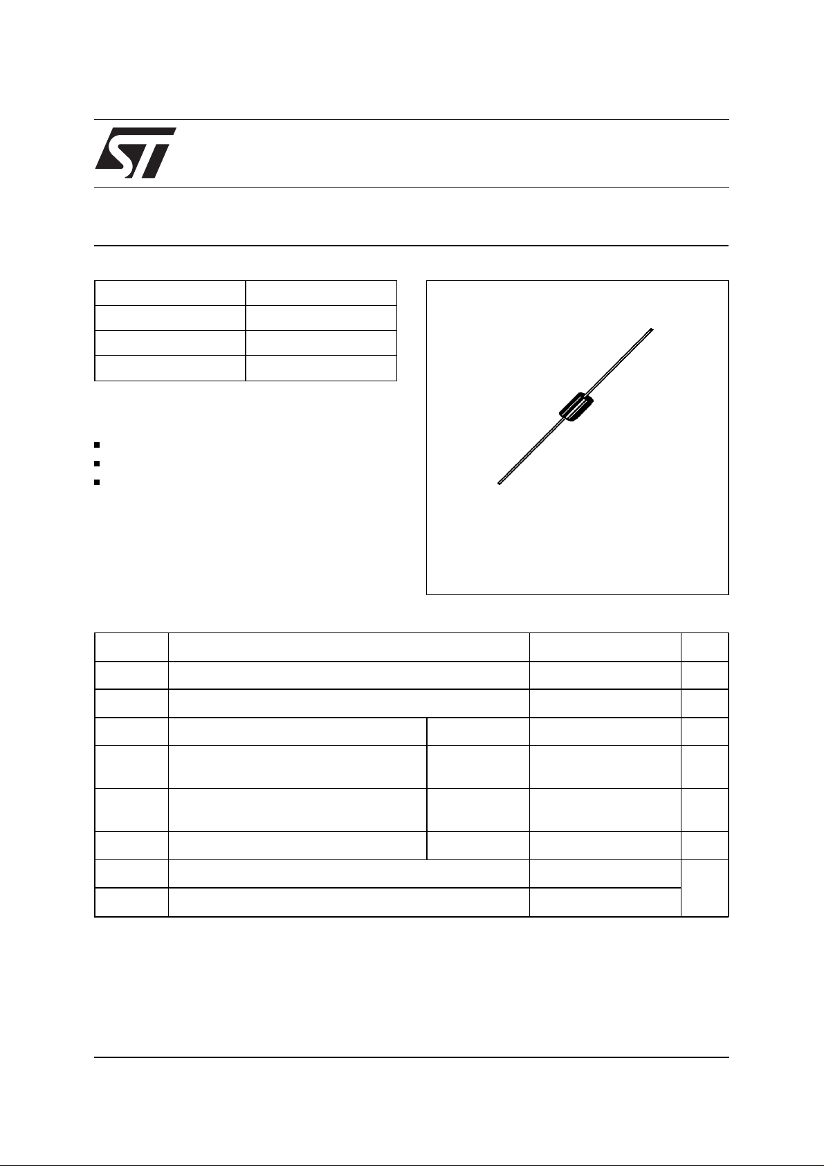
DO-201AD
(Plastic)
trol circuits.
Rectifier s in S.M. P.S.
ABSOLUTE RATINGS
(limiting values)
Symbol Parameter Value Unit
V
RRM
Repetitive peak reverse voltage
400 V
V
RSM
I
FRM
I
F (AV)
I
FSM
Non repetitive peak reverse voltage 400 V
Repetive peak forward current tp 10µs60A
Average forward current* T
Surge non repetitive forward current tp = 10ms
P Power dissipation * T
T
stg
T
Storage temperature range - 40 to + 150 °C
Maximum operating junction temperature
j
* On infinite heatsink with 10mm lead lengh.
October 1999 - Ed: 3B
a =
δ
= 0.5
65°C
3A
60 A
Sinusoidal
65°C 4.2 W
a =
+ 150
1/5
Page 2

BYT03-400
THERMAL RESISTANCES
Symbol Parameter Value Unit
R
th (j - a)
Junction-ambient* 20 °C/W
* On infinite heatsink with 10mm lead lengh.
STATIC ELECTRICAL CHARACTE RISTICS
Synbol Test Conditions Min. Typ. Max. Unit
I
R
V
F
Tj = 25C VR = V
= 100C 0.5 mA
T
j
RRM
Tj = 25C IF = 3A 1.5 V
= 100C 1.4
T
j
20
RECOVERY CHARA CTERISTICS
Symbol Test Conditions Min. Typ. Max. Unit
t
rr
Tj = 25C IF = 1A diF/dt = - 15A/µs VR = 30V 55 ns
µ
A
= 0.5A IR = 1 A Irr = 0.25A 25
I
F
TURN-OFF SWITCHING CHARAC TERISTICS
- Without series inductance
Symbol Test Conditions Min. Typ. Max. Unit
t
I
IRM
RM
diF/dt = - 50A/µsV
= 200 V IF = 3A
CC
≤
0.05µH T
L
p
= 100°C
j
diF/dt = -50A/µs 1.52A
35 50 ns
To evaluate the conduction losse use the following equations :
= 1.1 + 0.050 IF P = 1.1 x I
V
F
F(AV)
+ 0.050 I
F2(RMS)
2/5
Page 3

BYT03-400
Fig. 1:
Maximum average power dissipation
versus average forward current.
Fig.3 :
Thermal resistance versus lead length.
Fig. 2:
Average forward current versus ambient
temperature.
Fig. 4:
Transient thermal impedance junction
ambien t f o r m ou nt in g n° 2 ver s us p uls e d ur at io n
(L = 10 mm).
Fig. 5:
Peak forward current versus peak forward
voltage drop (maximum values).
3/5
Page 4

BYT03-400
Fig. 7:
Fig. 9:
Recovery time versus dI
F
/dt.
Peak reverse current versus dI
F
/dt.
Fig. 8:
Peak forward voltage versus dI
Fig. 10:
values).
Recovery charge versus dI
/dt.
F
/dt (typical
F
Fig. 11:
Dynamic parameters versus junction
temperature.
4/5
Fig. 12:
Non repetitive surge peak current versus
number of cycle.
Page 5

PACKAGE ME CHANICAL D AT A
DO-201AD (Plastic)
BA
BYT03-400
B
ØC
note 1
E
ØD ØD
DIMENSIONS
REF.
Millimeters Inches
Min. Max. Min. Max.
A 9.50 0.374
B 25.40 1.000
∅ C 5.30 0.209
∅ D 1.30 0.051
note 1
E
note 2
NOTES
1 - The lead diameter ∅ D is not controlled over zone E
2 - The minimum axial length within which the device may be
placed with its leads bent at right angles is 0.59"(15 mm)
E 1.25 0.049
Information furnished is believed to be accurate and reliable. However, STMicroelectronics assumes no responsibility for the consequences of
use of such information nor for any infringement of patents or other rights of third parties which may result from its use. No license is granted by
implication or otherwi se un der any pat ent or patent rights of STMic roelec tronics. S pecifications ment ioned in t his publ ication are subject to
change without notice. This publication supersedes and replaces all information previously supplied.
STMicroelectronics products are not author i zed f or use as critical comp onents i n l i fe s upport devices or systems without express written approval of STMicroelectronics.
The ST logo is a registered trademark of STMicroe lectronics
© 1999 STMicroelectronics - Printed in Italy - All rights reser ved.
STMicroelectronics GROUP OF COMPANIES
Australia - Brazil - China - Finland - France - Germany - Hong Kong - India - Italy - Japan - Malaysia
Malta - Morocco - Singapore - Spain - Sweden - Switzerland - United Kingdom - U.S.A.
http://www.st.com
5/5
 Loading...