

Page 1
DISCRETE SEMICONDUCTORS
DATA SH EET
ook, halfpage
M3D122
BYD11 series
Controlled avalanche rectifiers
Product specification
Supersedes data of April 1996
1996 Sep 26
Page 2

Philips Semiconductors Product specification
Controlled avalanche rectifiers BYD11 series
FEATURES
• Glass passivated
• High maximum operating
temperature
• Low leakage current
• Excellent stability
• Guaranteed avalanche energy
absorption capability
• Available in ammo-pack.
k
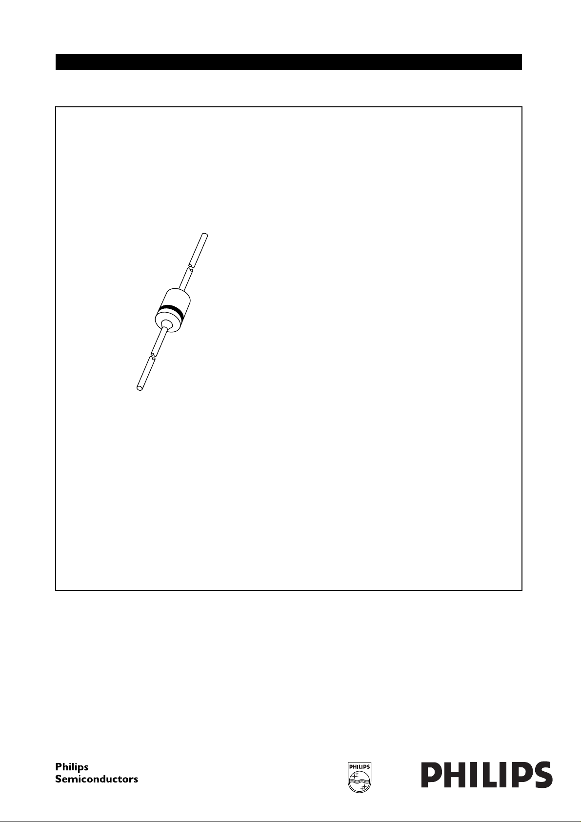
Fig.1 Simplified outline (SOD91) and symbol.
a
MAM196
DESCRIPTION
MARKING
Cavity free cylindrical glass package
(1)
through Implotec
technology.
This package is hermetically sealed
and fatigue free as coefficients of
expansion of all used parts are
matched.
(1) Implotec is a trademark of Philips.
BYD11D 11D
BYD11G 11G
BYD11J 11J
BYD11K 11K
BYD11M 11M
TYPE NUMBER MARKING CODE
LIMITING VALUES
In accordance with the Absolute Maximum Rating System (IEC 134).
SYMBOL PARAMETER CONDITIONS MIN. MAX. UNIT
V
RRM
repetitive peak reverse voltage
BYD11D − 200 V
BYD11G − 400 V
BYD11J − 600 V
BYD11K − 800 V
BYD11M − 1000 V
V
RWM
crest working reverse voltage
BYD11D − 200 V
BYD11G − 400 V
BYD11J − 600 V
BYD11K − 800 V
BYD11M − 1000 V
V
R
continuous reverse voltage
BYD11D − 200 V
BYD11G − 400 V
BYD11J − 600 V
BYD11K − 800 V
BYD11M − 1000 V
1996 Sep 26 2 Not recommended for new designs
Page 3

Philips Semiconductors Product specification
Controlled avalanche rectifiers BYD11 series
SYMBOL PARAMETER CONDITIONS MIN. MAX. UNIT
I
F(AV)
I
FSM
P
RSM
T
stg
T
j
average forward current Ttp=55°C;
lead length = 10 mm;
averaged over any 20 ms
period; see Figs 2 and 4
=60°C; PCB mounting
T
amb
(see Fig.9);
averaged over any 20 ms
period; see Figs 3 and 4
non-repetitive peak forward current t = 10 ms half sinewave;
non-repetitive peak reverse power
dissipation
Tj=T
VR=V
t=20µs half sinewave;
Tj=T
prior to surge;
j max
RRMmax
prior to surge
j max
storage temperature −65 +175 °C
junction temperature
see Fig.5
− 0.50 A
− 0.37 A
− 10 A
− 200 W
−65 +175 °C
ELECTRICAL CHARACTERISTICS
=25°C; unless otherwise specified.
T
j
SYMBOL PARAMETER CONDITIONS MIN. TYP. MAX. UNIT
tzt forward voltage
V
F
V
(BR)R
reverse avalanche
I
= 0.5 A; Tj=T
F
= 0.5 A; see Fig.6
I
F
IR= 0.1 mA
; see Fig.6
j max
−−0.91 V
−−1.06 V
breakdown voltage
BYD11D 225 −−V
BYD11G 450 −−V
BYD11J 650 −−V
BYD11K 900 −−V
BYD11M 1100 −−V
I
R
t
rr
reverse current
reverse recovery time
V
R=VRRMmax
V
R=VRRMmax
; see Fig.7
; Tj= 165 °C; see Fig.7
when switched from I
= 0.5 A to IR=1A;
F
−−1µA
−−75 µA
− 3 −
µs
measured at IR= 0.25 A; see Fig.10
C
d
diode capacitance
V
= 0 V; f = 1 MHz; see Fig.8
R
− 14 −
pF
THERMAL CHARACTERISTICS
SYMBOL PARAMETER CONDITIONS VALUE UNIT
R
R
th j-tp
th j-a
thermal resistance from junction to tie-point lead length = 10 mm 180 K/W
thermal resistance from junction to ambient note 1 250 K/W
Note
1. Device mounted on epoxy-glass printed-circuit board, 1.5 mm thick; thickness of copper ≥40 µm, see Fig.9.
For more information please refer to the
“General Part of associated Handbook”
.
1996 Sep 26 3 Not recommended for new designs
Page 4
Philips Semiconductors Product specification
Controlled avalanche rectifiers BYD11 series
GRAPHICAL DATA
0.8
handbook, halfpage
I
F(AV)
(A)
0.6
0.4
0.2
0
0 40 200
a =1.57; VR=V
Lead length 10 mm.
RRMmax
80 120 160
; δ = 0.5.
MBG042
Ttp (
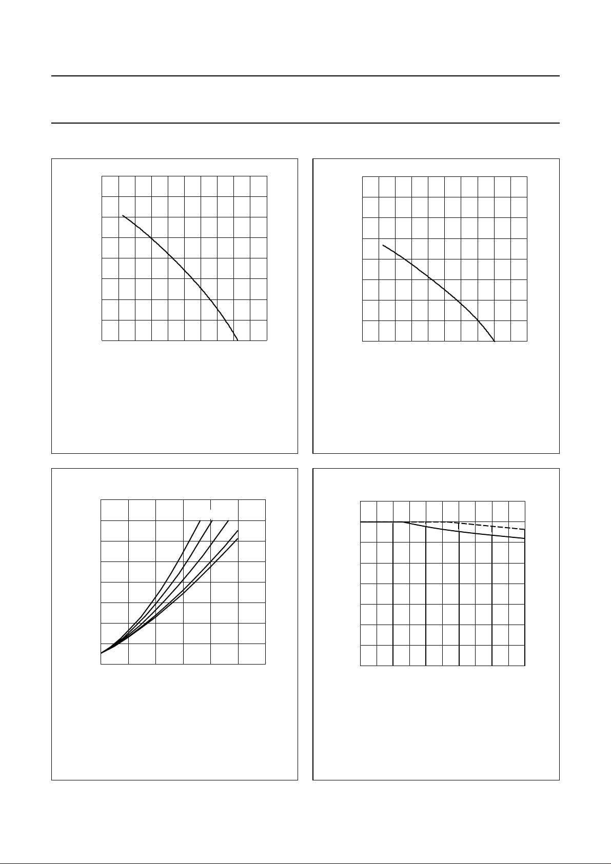
Fig.2 Maximum permissible average forward
current as a function of tie-point
temperature (including losses due to
reverse leakage).
T
amb
MBG051
o
(
C)
0.8
handbook, halfpage
I
F(AV)
(A)
0.6
0.4
0.2
0
o
C)
a = 1.57; VR=V
Device mounted as shown in Fig.9.
0 40 200
RRMmax
80 120 160
; δ = 0.5.
Fig.3 Maximum permissible average forward
current as a function of ambient
temperature (including losses due to
reverse leakage).
I
F (AV)
MBG634
1.57
1.42
(A)
0.8
handbook, halfpage
P
(W)
0.6
0.4
0.2
0
0 0.2 0.4 0.6
a=I
F(RMS)/IF(AV)
; VR=V
RRMmax
; δ = 0.5.
a = 3
2.5 2
Fig.4 Maximum steady state power dissipation
(forward plus leakage current losses,
excluding switching losses) as a function of
average forward current.
200
handbook, halfpage
T
j
o
( C)
100
0
0 500 1000
Solid line = VR.
Dotted line = V
DGJKM
VR(V)
; δ = 0.5.
RRM
MCD583
Fig.5 Maximum permissible junction temperature
as a function of reverse voltage.
1996 Sep 26 4 Not recommended for new designs
Page 5
Philips Semiconductors Product specification
Controlled avalanche rectifiers BYD11 series
handbook, halfpage
4
I
F
(A)
3
2
1
0
0
Solid line: Tj=25°C.
Dotted line: Tj= 175 °C.
MBG047
VF (V)
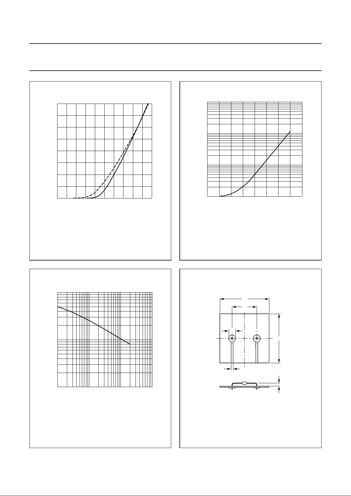
Fig.6 Forward current as a function of forward
voltage; maximum values.
o
()
MCD582
2000 100
3
10
handbook, halfpage
I
R
(µA)
2
10
10
VR=V
1
RRMmax
TjC
.
21
Fig.7 Reverse current as a function of junction
temperature; maximum values.
VR (V)
MBG025
handbook, halfpage
3
10
Dimensions in mm.
50
25
7
50
2
3
MGA200
1
10
handbook, halfpage
C
d
(pF)
1
−1
10
1
f = 1 MHz; Tj=25°C.
10 10
2
Fig.8 Diode capacitance as a function of reverse
voltage; typical values.
Fig.9 Device mounted on a printed-circuit board.
1996 Sep 26 5 Not recommended for new designs
Page 6
Philips Semiconductors Product specification
Controlled avalanche rectifiers BYD11 series
I
I
(A)
0.25
R
(A)
0.5
0.5
1.0
F
t
rr
0
t
MAM057
handbook, full pagewidth
10 Ω
DUT
+
25 V
1 Ω
50 Ω
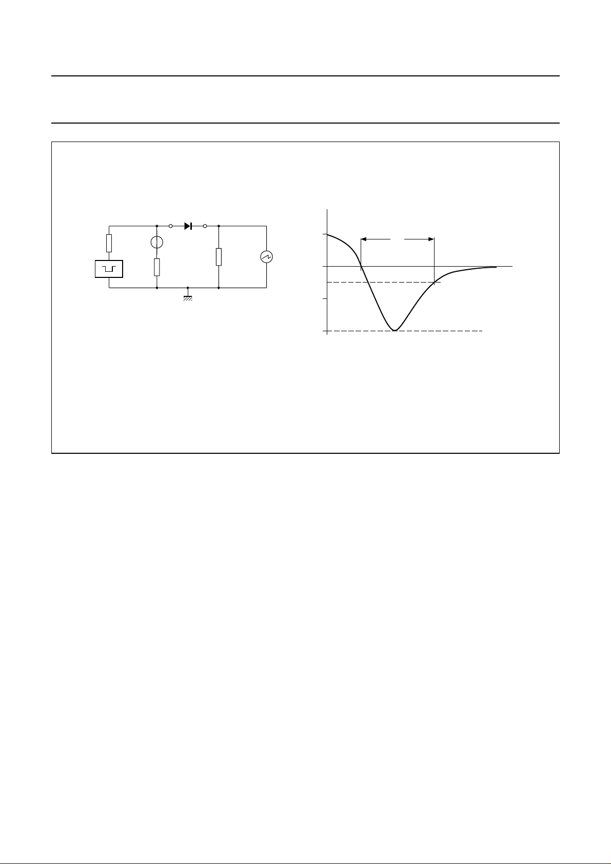
Input impedance oscilloscope: 1 MΩ, 22 pF; tr≤ 7 ns.
Source impedance: 50 Ω; tr≤ 15 ns.
Fig.10 Test circuit and reverse recovery time waveform and definition.
1996 Sep 26 6 Not recommended for new designs
Page 7
Philips Semiconductors Product specification
Controlled avalanche rectifiers BYD11 series
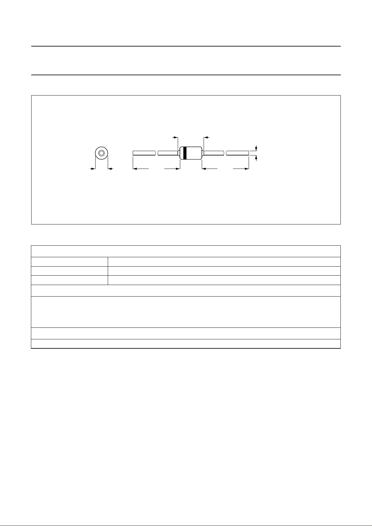
PACKAGE OUTLINE
handbook, full pagewidth
1.7
max
Dimensions in mm.
The marking band indicates the cathode.
29 min 29 min3.0 max
3.5 max
0.55
max
MBC053
Fig.11 SOD91.
DEFINITIONS
Data sheet status
Objective specification This data sheet contains target or goal specifications for product development.
Preliminary specification This data sheet contains preliminary data; supplementary data may be published later.
Product specification This data sheet contains final product specifications.
Limiting values
Limiting values given are in accordance with the Absolute Maximum Rating System (IEC 134). Stress above one or
more of the limiting values may cause permanent damage to the device. These are stress ratings only and operation
of the device at these or at any other conditions above those given in the Characteristics sections of the specification
is not implied. Exposure to limiting values for extended periods may affect device reliability.
Application information
Where application information is given, it is advisory and does not form part of the specification.
LIFE SUPPORT APPLICATIONS
These products are not designed for use in life support appliances, devices, or systems where malfunction of these
products can reasonably be expected to result in personal injury. Philips customers using or selling these products for
use in such applications do so at their own risk and agree to fully indemnify Philips for any damages resulting from such
improper use or sale.
1996 Sep 26 7 Not recommended for new designs
 Loading...