

Page 1
Philips Semiconductors Objective specification
Silicon Diffused Power Transistor BUJ101A
GENERAL DESCRIPTION
High-voltage, high-speed planar-passivated npn power switching transistor in TO220AB envelope intended for use
in high frequency electronic lighting ballast applications, converters, inverters, switching regulators, motor control
systems, etc.
QUICK REFERENCE DATA
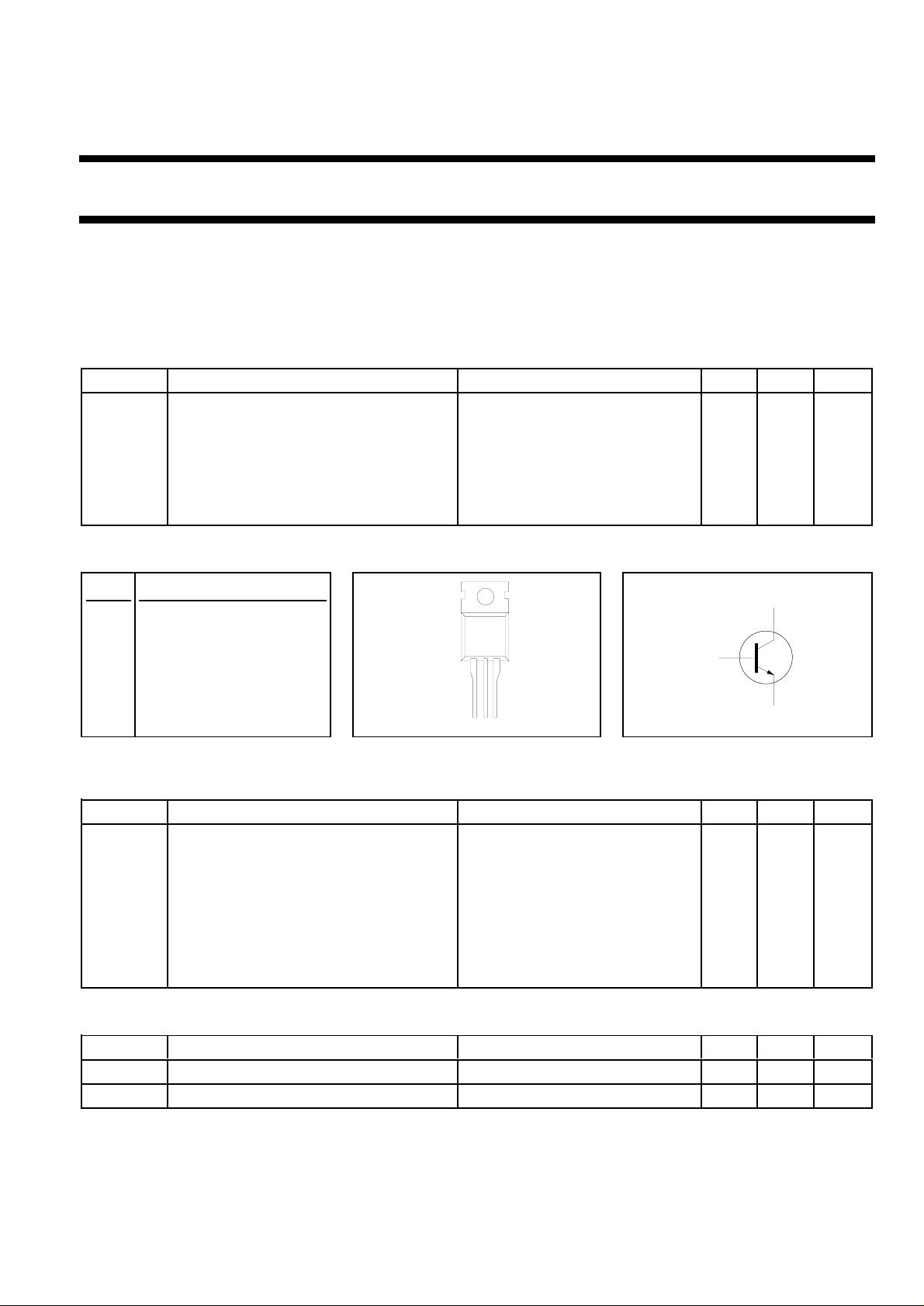
SYMBOL PARAMETER CONDITIONS TYP. MAX. UNIT
V
CESM
V
CBO
V
CEO
I
C
I
CM
P
tot
V
CEsat
t
f
PINNING - TO220AB PIN CONFIGURATION SYMBOL
Collector-emitter voltage peak value VBE = 0 V - 700 V
Collector-Base voltage (open emitter) - 700 V
Collector-emitter voltage (open base) - 400 V
Collector current (DC) - 0.5 A
Collector current peak value - 1 A
Total power dissipation Tmb ≤ 25 ˚C - 42 W
Collector-emitter saturation voltage IC = 0.2 A;IB = 20 mA - 1.0 V
Fall time Ic=0.2A,IB1=20mA 40 100 ns
PIN DESCRIPTION
tab
c
1 base
2 collector
b
3 emitter
tab collector
123
LIMITING VALUES
Limiting values in accordance with the Absolute Maximum Rating System (IEC 134)
SYMBOL PARAMETER CONDITIONS MIN. MAX. UNIT
V
V
V
I
C
I
CM
I
B
I
BM
P
T
T
CESM
CEO
CBO
tot
stg
j
Collector to emitter voltage VBE = 0 V - 700 V
Collector to emitter voltage (open base) - 400 V
Collector to base voltage (open emitter) - 700 V
Collector current (DC) - 0.5 A
Collector current peak value - 1 A
Base current (DC) - 0.2 A
Base current peak value - 0.3 A
Total power dissipation Tmb ≤ 25 ˚C - 42 W
Storage temperature -65 150 ˚C
Junction temperature - 150 ˚C
THERMAL RESISTANCES
e
SYMBOL PARAMETER CONDITIONS TYP. MAX. UNIT
R
R
th j-mb
th j-a
Junction to mounting base - 3.0 K/W
Junction to ambient in free air 100 - K/W
August 1998 1 Rev 1.000
Page 2
Philips Semiconductors Objective specification
Silicon Diffused Power Transistor BUJ101A
STATIC CHARACTERISTICS
Tmb = 25 ˚C unless otherwise specified
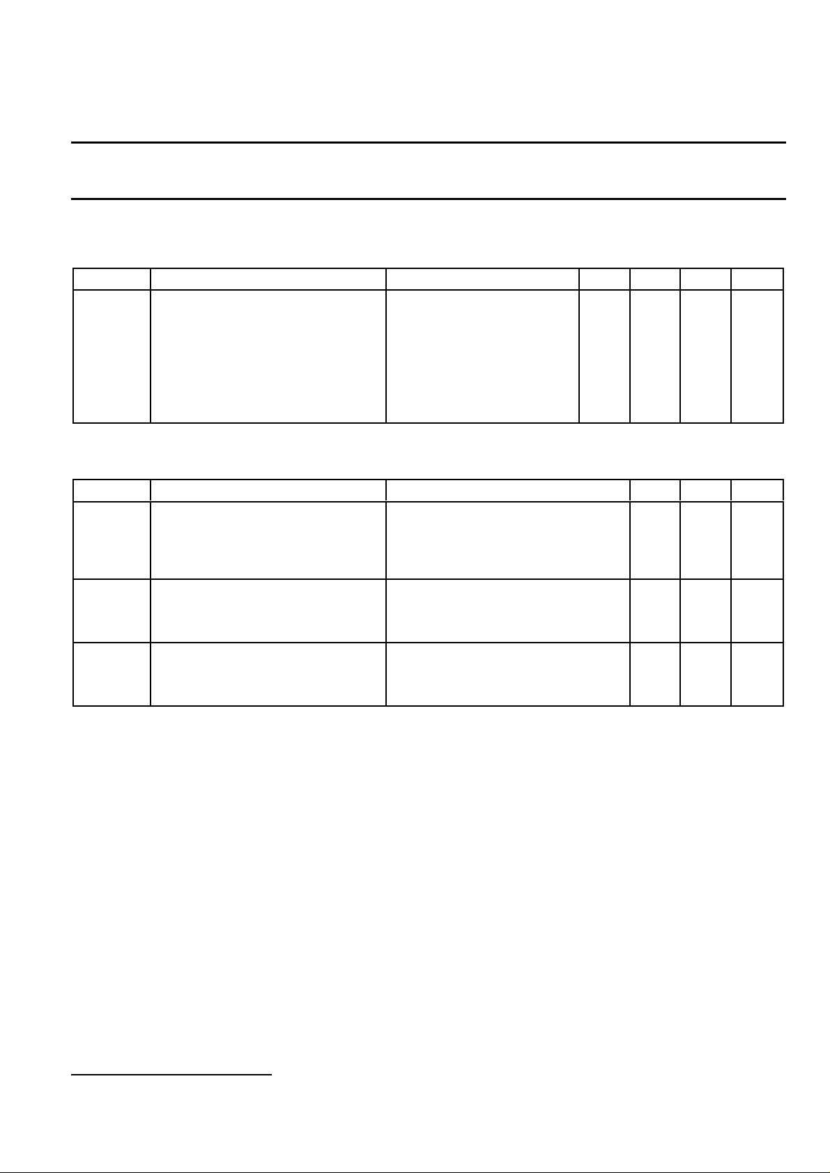
SYMBOL PARAMETER CONDITIONS MIN. TYP. MAX. UNIT
I
CES
I
CES
I
EBO
V
CEOsust
V
CEsat
V
BEsat
h
FE
Collector cut-off current
Emitter cut-off current VEB = 5 V; IC = 0 A - - 1 mA
Collector-emitter sustaining voltage IB = 0 A; IC = 100 mA; 400 - - V
Collector-emitter saturation voltage IC = 0.1 A; IB = 10 mA - - 0.8 V
Base-emitter saturation voltage IC = 0.2 A; IB =20 mA - - 1.0 V
DC current gain IC = 1 mA; VCE = 5 V 10 - 32
DYNAMIC CHARACTERISTICS
Tmb = 25 ˚C unless otherwise specified
SYMBOL PARAMETER CONDITIONS TYP. MAX. UNIT
Switching times (resistive load) I
t
on
t
s
t
f
t
s
t
f
t
s
t
f
Turn-on time - 0.5 µs
Turn-off storage time - 3 µs
Turn-off fall time - 0.3 µs
Switching times (inductive load) I
Turn-off storage time - 1.5 µs
Turn-off fall time 40 100 ns
Switching times (inductive load) I
Turn-off storage time - 1.8 µs
Turn-off fall time - 200 ns
1
VBE = 0 V; VCE = V
VBE = 0 V; VCE = V
Tj = 125 ˚C
CESMmax
; - - 1.0 mA
CESMmax
- - 0.1 mA
L = 25 mH
= 0.2 A; I
Con
RL = 75 ohms; V
= 0.2 A; I
Con
-VBB = 5 V
= 0.2 A; I
Con
-VBB = 5 V; Tj = 100 ˚C
= -I
Bon
Bon
Bon
= 20 mA;
Boff
= 4 V;
BB2
= 20m A; LB = 1 µH;
= 20m A; LB = 1 µH;
1 Measured with half sine-wave voltage (curve tracer).
August 1998 2 Rev 1.000
Page 3
Philips Semiconductors Objective specification
Silicon Diffused Power Transistor BUJ101A
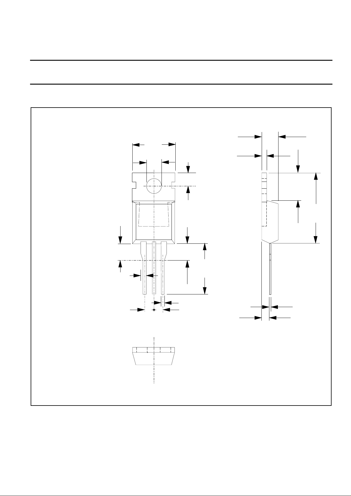
MECHANICAL DATA
Dimensions in mm
Net Mass: 2 g
10,3
max
1,3
3,7
4,5
max
3,0 max
not tinned
1,3
max
(2x)
123
2,54 2,54
2,8
3,0
13,5
min
0,9 max (3x)
5,9
min
15,8
max
0,6
2,4
Fig.1. TO220AB; pin 2 connected to mounting base.
Notes
1. Refer to mounting instructions for TO220 envelopes.
2. Epoxy meets UL94 V0 at 1/8".
August 1998 3 Rev 1.000
Page 4

Philips Semiconductors Objective specification
Silicon Diffused Power Transistor BUJ101A
DEFINITIONS
Data sheet status
Objective specification This data sheet contains target or goal specifications for product development.
Preliminary specification This data sheet contains preliminary data; supplementary data may be published later.
Product specification This data sheet contains final product specifications.
Limiting values
Limiting values are given in accordance with the Absolute Maximum Rating System (IEC 134). Stress above one
or more of the limiting values may cause permanent damage to the device. These are stress ratings only and
operation of the device at these or at any other conditions above those given in the Characteristics sections of
this specification is not implied. Exposure to limiting values for extended periods may affect device reliability.
Application information
Where application information is given, it is advisory and does not form part of the specification.
Philips Electronics N.V. 1998
All rights are reserved. Reproduction in whole or in part is prohibited without the prior written consent of the
copyright owner.
The information presented in this document does not form part of any quotation or contract, it is believed to be
accurate and reliable and may be changed without notice. No liability will be accepted by the publisher for any
consequence of its use. Publication thereof does not convey nor imply any license under patent or other
industrial or intellectual property rights.
LIFE SUPPORT APPLICATIONS
These products are not designed for use in life support appliances, devices or systems where malfunction of these
products can be reasonably expected to result in personal injury. Philips customers using or selling these products
for use in such applications do so at their own risk and agree to fully indemnify Philips for any damages resulting
from such improper use or sale.
August 1998 4 Rev 1.000
 Loading...