

Page 1

BU208A
HIGH VOLTAGE FAST-SWITCHING
■ STMicroelectronicsPREFERRED
SALESTYPES
■ HIGH VOLTAGE CAPABILITY
■ U.L.RECOGNISEDISOWATT218 PACKAGE
(U.L. FILE # E81734 (N)
■ JEDEC TO-3 METAL CASE.
APPLICATIONS:
■ HORIZONTALDEFLECTIONFOR COLOUR
TV
DESCRIPTION
The BU208A, BU508A and BU508AFI are
manufactured using Multiepitaxial Mesa
technology for cost-effective high performance
and use a Hollow Emitter structure to enhance
switchingspeeds.
BU508A/BU508AFI
NPN POWER TRANSISTORS
TO-3
1
2
3
2
TO-218 ISOWATT218
1
3
2
1
INTERNAL SCHEMATIC DIAGRAM
For TO-3 :
C = Tab
E = Pin2.
ABSOLUTE MAXIMUM RATINGS
Symbol Parameter Value Unit
V
V
V
I
P
T
Collect or-Emitter Voltage (VBE=0) 1500 V
CES
Collect or-Emitter Voltage (IB= 0) 700 V
CEO
Emitter-Base Voltage (IC=0) 10 V
EBO
Collect or Current 8 A
I
C
Collect or Peak Current (tp<5ms) 15 A
CM
TO - 3 TO - 218 ISOWATT218
Tot al Dissipation at Tc=25oC 150 125 50 W
tot
Storage Temp erature -65 to 175 -65 to 150 -65 to 150
stg
Max. Ope r ating Jun ct ion Te m pe rature 175 150 150
T
j
o
C
o
C
November 1999
1/8
Page 2

BU208A / BU508A / BU508AFI
THERMAL DATA
R
thj-case
Ther mal Res ist ance J unctio n-c a s e Max 1 1 2.5
TO-3 TO-218 ISOWA TT218
o
C/W
ELECTRICAL CHARACTERISTICS (T
=25oC unlessotherwisespecified)
case
Symbol Parameter Test Cond itions Min. Typ. Max. Unit
I
CES
I
EBO
V
CEO(sus)
Collec t or Cut -off
Current (V
BE
=0)
Emitt er Cut -off Current
(I
=0)
C
∗ Collect or- Emit t er
V
= 1500 V TC=125oC
CE
= 1500 V
V
CE
=5V 100 µA
V
EB
I
= 100 m A 700 V
C
1
2
Sust aining Voltage
=0)
(I
B
V
EBO
Emit ter Base Volta ge
(I
∗ Co llector-Emit t er
V
CE(sat)
C
=0)
I
=10mA 10 V
E
IC=4.5A IB=2A 1 V
Saturation Voltage
∗ Ba se- Emitt er
V
BE(sat)
IC=4.5A IB=2A 1.3 V
Saturation Voltage
INDUCTIVE LOAD
t
f
∗
Pulsed: Pulse duration = 300 µs, duty cycle1.5 %
Storage Ti me
s
t
Fall Time
f
Tr ansition Freque n cy IC=0.1A VCE= 5 V f = 5 MHz 7 MHz
T
IC=4.5A hFE=2.5 VCC=140V
=0.9mH LB=3µH
L
C
7
0.55
mA
mA
µs
µs
Safe Operating Area(TO-3) Safe Operating Areas (TO-218/ISOWATT218)
2/8
Page 3
BU208A / BU508A / BU508AFI
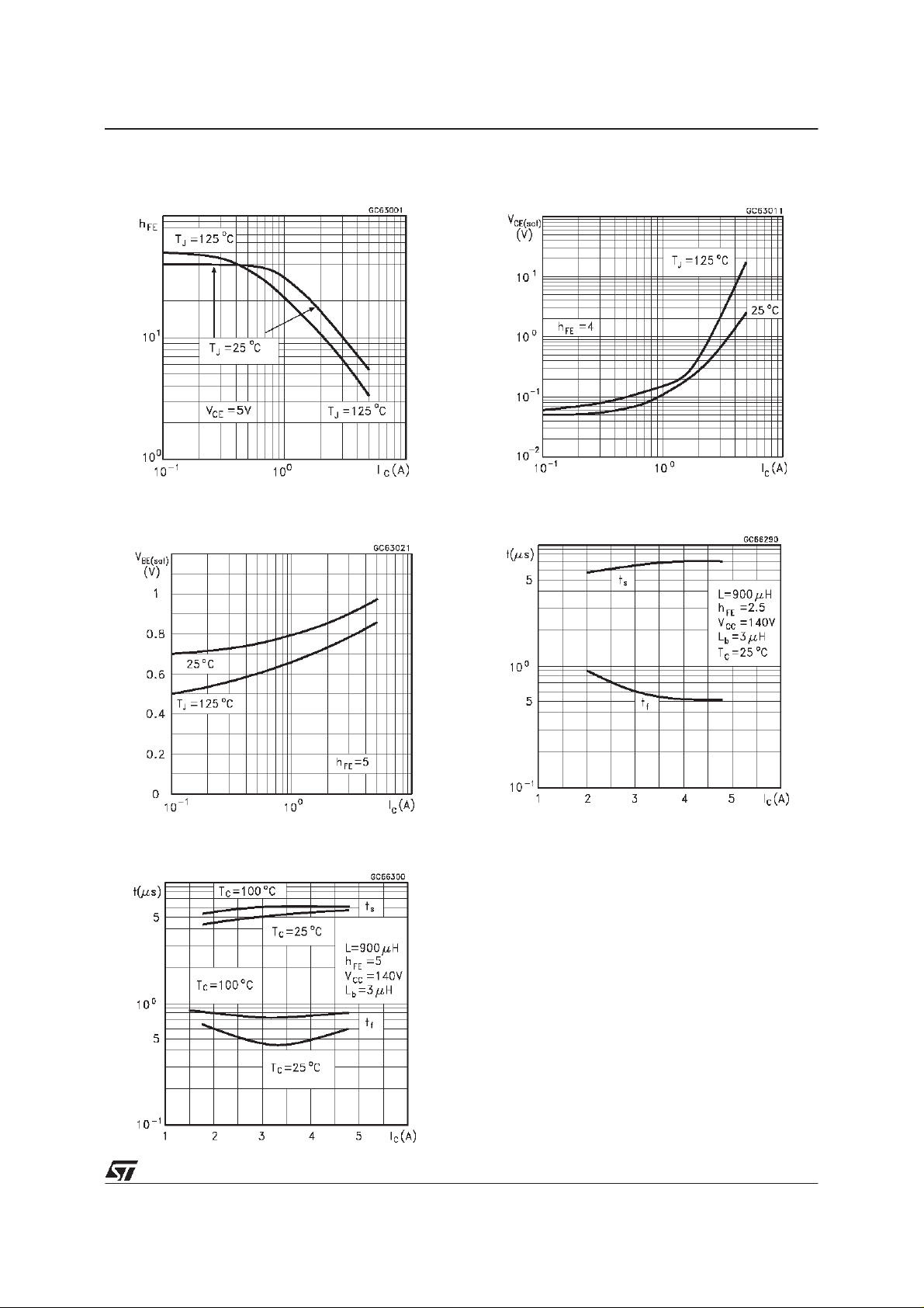
DCCurrent Gain
Base Emitter SaturationVoltage
Collector EmitterSaturation Voltage
SwitchingTime Inductive Load
SwitchingTime InductiveLoad (see figure 1)
3/8
Page 4

BU208A / BU508A / BU508AFI
Figure1: Inductive Load Switching TestCircuit.
4/8
Page 5

TO-3 MECHANICAL DATA
BU208A / BU508A / BU508AFI
DIM.
mm inch
MIN. TYP. MAX. MIN. TYP. MAX.
A 11.00 13.10 0.433 0.516
B 0.97 1.15 0.038 0.045
C 1.50 1.65 0.059 0.065
D 8.32 8.92 0.327 0.351
E 19.00 20.00 0.748 0.787
G 10.70 11.10 0.421 0.437
N 16.50 17.20 0.649 0.677
P 25.00 26.00 0.984 1.023
R 4.00 4.09 0.157 0.161
U 38.50 39.30 1.515 1.547
V 30.00 30.30 1.187 1.193
P
G
U
V
N
O
R
B
DA
C
E
P003F
5/8
Page 6

BU208A / BU508A / BU508AFI
TO-218 (SOT-93) MECHANICAL DATA
DIM.
MIN. TYP. MAX. MIN. TYP. MAX.
A 4.7 4.9 0.185 0.193
C 1.17 1.37 0.046 0.054
D 2.5 0.098
E 0.5 0.78 0.019 0.030
F 1.1 1.3 0.043 0.051
G 10.8 11.1 0.425 0.437
H 14.7 15.2 0.578 0.598
L2 – 16.2 – 0.637
L3 18 0.708
L5 3.95 4.15 0.155 0.163
L6 31 1.220
R – 12.2 – 0.480
Ø 4 4.1 0.157 0.161
mm inch
E
A
C
L5
D
L6
L3
L2
H
G
¯
F
R
123
P025A
6/8
Page 7

BU208A / BU508A / BU508AFI
ISOWATT218MECHANICAL DATA
DIM.
A 5.35 5.65 0.211 0.222
C 3.30 3.80 0.130 0.150
D 2.90 3.10 0.114 0.122
D1 1.88 2.08 0.074 0.082
E 0.75 0.95 0.030 0.037
F 1.05 1.25 0.041 0.049
F2 1.50 1.70 0.059 0.067
F3 1.90 2.10 0.075 0.083
G 10.80 11.20 0.425 0.441
H 15.80 16.20 0.622 0.638
L 9 0.354
L1 20.80 21.20 0.819 0.835
L2 19.10 19.90 0.752 0.783
L3 22.80 23.60 0.898 0.929
L4 40.50 42.50 1.594 1.673
L5 4.85 5.25 0.191 0.207
L6 20.25 20.75 0.797 0.817
N 2.1 2.3 0.083 0.091
R 4.6 0.181
DIA 3.5 3.7 0.138 0.146
MIN. TYP. MAX. MIN. TYP. MAX.
mm inch
- Weight: 4.9g (typ.)
- MaximumTorque(applied to mounting flange) Recommended: 0.8Nm; Maximum:1 Nm
- Theside of thedissipatormust beflat within 80 µm
P025C/A
7/8
Page 8

BU208A / BU508A / BU508AFI
Information furnished is believed tobe accurate andreliable. However, STMicroelectronics assumes no responsibility for the consequences
of use of such information nor for any infringement of patents or other rights of third parties which may result from its use. No license is
granted by implication or otherwise under any patent or patent rights of STMicroelectronics. Specification mentioned in this publication are
subject to change without notice. This publication supersedes and replaces all information previously supplied. STMicroelectronics products
are not authorized for use as critical components in life support devices or systems without express written approval of STMicroelectronics.
The ST logo is a trademark of STMicroelectronics
1999 STMicroelectronics – Printed in Italy – All Rights Reserved
STMicroelectronicsGROUP OF COMPANIES
Australia - Brazil - China - Finland - France - Germany - Hong Kong - India- Italy- Japan - Malaysia - Malta - Morocco -
Singapore- Spain - Sweden - Switzerland -United Kingdom - U.S.A.
http://www.st.com
.
8/8
 Loading...