

Page 1

1
Standard ICs
Dual precision monostable
multivibrator
BU4538B
The BU4538B is a monostable multivibrator that can be reset and retriggered. It is triggered from either edge of an
input pulse. As the output pulse width and accuracy are determined by the external timing constants Cx and Rx, a
wide range of accurate output pulse widths is available. Linear CMOS technology makes it possible to control the
output pulse width with greater accuracy. Determination is made based on t
WOUT = Rx · Cx throughout the entire
power supply voltage range, eliminating the necessity for other coefficients.
•
Features
1) Low power dissipation.
2) Wide range of operating power supply voltages.
3) High input impedance.
4) High fan-out.
5) Direct drive of 2 L-TTL inputs and 1 LS-TTL input.
•
Block diagram
•
Logic circuit diagram
2
T
2A
T1A
AA
BA
QA
Q
C
D
T1
T2
Q
QA
CDA
3
4
5
6
7
8
15
14
13
12
11
10
9
V
SS
1
T
1B
VDD
CDB
AB
BB
QB
T2B
QB
16
BA
Q
C
D
T1
T2
Q
BA
VDD
RX
2 (14)
1 (15)
4 (12)
T
1
Vref1 Enable
S
R
V
ref2
Reset Latch
QQ
Enable
A
B
C
X
VDD
Control
Output
Latch
QS
QR
T2
CD
5 (11)
3 (13)
6 (10)
7 (9)
•
Truth table
INPUT OUTPUT
ABC
D Q
Q
HH
LH L H
HLH
LH
XXL L H
H
Page 2
2
Standard ICs BU4538B
•
Absolute maximum ratings (Ta = 25°C, VSS = 0V)
Parameter Symbol Limits Unit
V
DD – 0.3 ~ + 18 V
mW
°C
°C
V
IN – 0.3 ~ VDD + 0.3 V
1000 (DIP)
– 55 ~ + 150
– 40 ~ + 85
Pd
Topr
Tstg
Power supply voltage
Power dissipation
Operating temperature
Storage temperature
Input voltage
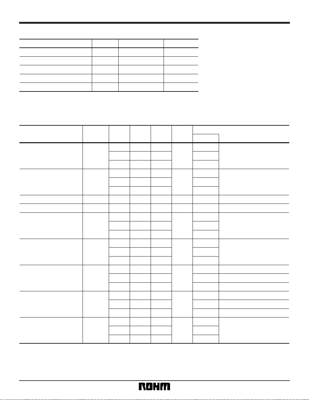
Parameter Symbol Min. Typ. Max. Unit Conditions
V
IH
3.5
——
V
5
—
7.0
——
10
11.0
——
15
V
IL
——
1.5
V
5
———
3.0 10
——
4.0 15
I
IH
——
0.3 µ
A15V
IH = 15V
I
IL
——
– 0.3 µ
A15V
IL = 0V
V
OH
4.95
——
V
5
I
O = 0mA9.95
——
10
14.95
——
15
V
OL
——
0.05
V
5
I
O = 0mA
——
0.05 10
——
0.05 15
I
OH
– 0.16
——
mA
5VOH = 4.6V
– 0.4
——
10 V
OH = 9.5V
– 1.2
——
15 V
OH = 13.5V
I
OL
0.44
——
mA
5VOL = 0.4V
1.1
——
10 V
OL = 0.5V
3.0
——
15 V
OL = 1.5V
I
DD
——
20
µ
A
5
V
I = VDD or GND
——
40 10
——
80 15
V
DD (V)
Input high level voltage
Input low level voltage
Input high level current
Input low level current
Output high level voltage
Output low level voltage
Output high level current
Output low level current
Static current dissipation
•
Electrical characteristics
DC characteristics (unless otherwise noted, Ta = 25°C, V
SS = 0V)
Page 3

3
Standard ICs BU4538B
Parameter Symbol Min. Typ. Max. Unit Conditions
t
TLH
— 100 —
ns
5
—— 50 — 10
— 40 — 15
t
THL
— 100 —
ns
5
—— 50 — 10
— 40 — 15
t
PLH
tPHL
— 300 —
ns
5
—— 150 — 10
— 100 — 15
t
PLH
tPHL
— 250 —
ns
5
—
— 125 — 10
— 95 — 15
t
WIN
— 50 —
ns
5
—— 30 — 10
— 25 — 15
t
WOUT1
185 200 215
µ
s
5
185 200 215 10
185 200 215 15
t
WOUT2
8.8 9.4 10.0
ms
5
8.8 9.4 10.0 10
8.8 9.4 10.0 15
t
rr
— 0 —
ns
5
—— 0 — 10
— 0 — 15
C
IN — 5 — pF ——
C
X = 2000pF, RX = 100kΩ
C
X = 0.1µ
F, R
X = 100kΩ
VDD (V)
Output rise time
Output fall time
Propagation delay
time A, B to Q, Q
Propagation delay
time C
D to Q, Q
Minimum input
pulse width
Output pulse width 1
Output pulse width 2
Minimum retrigger
time
Input capacitance
Switching characteristics (unless otherwise noted, Ta = 25°C, CL = 50pF, VSS = 0V)
•
Recommended operating conditions
Parameter Symbol Min. Typ. Max. Unit Conditions
R
X 5
—
1000 k
Ω
—
C
X No Limit pF
—
External timing resistance
External timing capacitance
Page 4

4
Standard ICs BU4538B
•
Timing chart
tW tW t2 t3 tW
t1
A
B
C
D
Q
Q
t1, t2, t3 < tW
•
Measurement circuits
P. G.
P. G.
P. G. CLCL
VDD
RX
CX
CD
A
V
DD T2 T1
B
Q
Q
Fig. 1 (a) Switching time
VSS
A
B
C
D
Q
Q
50%
90%
50%
10%
20ns
20ns
50%
50%
50%
50%
50%
50%
50%
50%
20ns
20ns
t
rr
90%
10%
90%
50%
10%
20ns
20ns
tPLH
tPHL
tPHL
tWOUT
tPLH
tTHL
tTLH
tTLH
tPHL
tTHL
tPHL
90%
90%
10%
10%
90%
10%
50%
tWOUT
Fig. 1 (b) Switching time measurement waveforms
Page 5

5
Standard ICs BU4538B
POWER DISSIPATION: Pd (mW)
1200
1000
800
600
400
200
0
0255075100125150
AMBIENT TEMPERATURE: Ta (°C)
Fig. 2 Power dissipation vs. Ta
•
Electrical characteristic curve
DIP16
0.51Min.
0.3
± 0.1
916
81
6.5 ± 0.3
3.2
±
0.2
4.25
±
0.3
0.5 ± 0.1
19.4 ± 0.3
2.54
0° ~ 15°
7.62
•
External dimensions (Units: mm)
 Loading...