

Page 1
1
Standard ICs
8-bit serial in, parallel out driver IC
BU2050F
The BU2050F is a driver IC that is comprised of an 8-bit shift register and a latch (serial in / parallel out). The data
read into the shift register can be asynchronously latched. The CMOS outputs can provide 25mA (Max.) of current
per output, making this IC ideal for a wide range of applications including driving LED
S.
•
Applications
Printers, mini-component stereo systems, car audio systems, and musical instruments
•
Features
1) Regardless of the clock and data input, the CLR pin
resets the latch circuit, and sets all outputs to the low
level.
2) Output drive capacity: 25mA / output (Max.).
3) Input pin hysteresis: 0.5V (Typ.).
•
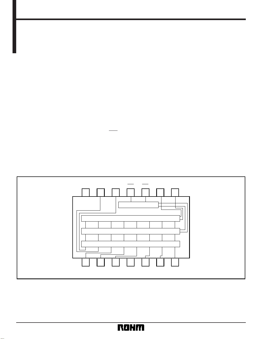
Block diagram
11
CLR10STB9CLK8DATA
12
P1
13
P2
14
4567321
V
DD
VSS P6 P7 P8P5P4P3
SHIFT REGISTER
LATCH
OUTPUT Driver
CTRL
Page 2
2
Standard ICs BU2050F
•
Pin descriptions
Pin No.
1
Pin name
Function
P3 Parallel data output
Parallel data output
Parallel data output
GND
Parallel data output
Parallel data output
Parallel data output
Serial data input
Clock signal input
Strobe signal input
When STB is low, the contents of the shift register are output.
When STB is high, the contents of the latch circuit and output do not change.
Reset signal input
When CLR is low, the latch circuit is reset, and all outputs (P1 to P8) are set to low.
Normally, CLR is high.
Parallel data output
Parallel data output
Power supply voltage
2P4
3P5
4V
SS
5P6
6P7
7P8
8 DATA
9 CLK
10 STB
11 CLR
12 P1
13 P2
14 V
DD
•
Absolute maximum ratings (Ta = 25°C)
Parameter Symbol Limits
– 0.3 ~ + 7.0
V
SS – 0.3 ~ VDD + 0.5
V
SS – 0.3 ~ VDD + 0.5
Unit
V
mA
V
V
DD
ISINK
Vo
Power supply voltage
Input voltage
450 mWPdPower dissipation
∗
1
output voltage
– 25 ~ + 85
°C
Topr
– 55 ~ + 125
°CTstgStorage temperature
Operating temperature
Note: These voltage value ranges are the destruction limits for the IC. They are not the guaranteed operating ranges for the IC.
∗
1 Reduced by 4.5mW for each increase in Ta of 1°C over 25°C.
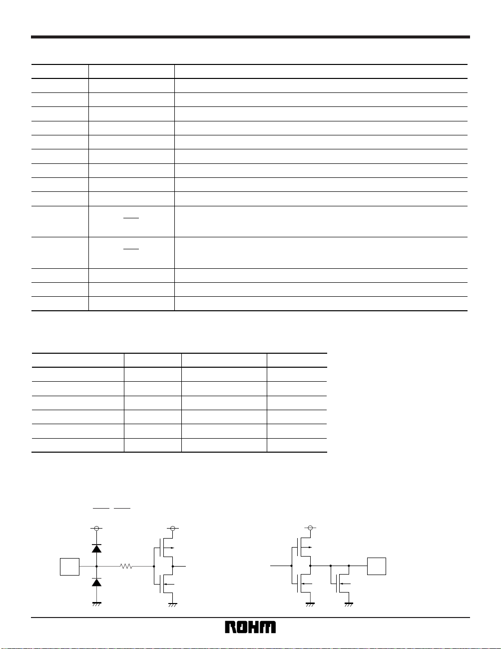
•
Input / output circuits
(1) DATA, CLK, STB, CLR (2) P1 ~ P8
Page 3

3
Standard ICs BU2050F
•
Electrical characteristics (unless otherwise noted, VDD = 4.5V ~ 5.5V, Ta = 25°C)
Parameter
Symbol Min. Typ. Max. Unit Conditions
Power supply current
Input high level voltage
Input low level voltage
Input leak current
Output high level voltage
Output low level voltage
I
DD
VIH
VIL
ILI
VOHD
VOLD
—
0.7V
DD
VSS
– 10
V
DD – 1.5
V
DD – 1.0
V
DD – 0.5
V
SS
VSS
VSS
— 0.1 mA
—V
DD V
— 0.3V
DD V
—10µA
—V
DD V
—V
DD V
—V
DD V
— 1.5 V
— 0.8 V
— 0.4 V
V
IH = VDD, VIL = VSS
—
—
V
1 = 0 ~ VDD
IOH = – 25mA
I
OH = – 15mA
I
OH = – 10mA
I
OL = + 25mA
I
OL = + 15mA
I
OL = + 10mA
•
Switching characteristics (unless otherwise noted, VDD = 4.5V ~ 5.5V, Ta = 25°C)
Parameter
Symbol Min. Typ. Max. Unit Conditions
Hold time
(STB-CLK)
Transmission delay time
(CLK-P1 ~ P8)
Transmission delay time
(STB-P1 ~ P8)
Transmission delay time
(CLR-P1 ~ P8)
Max. operating frequency
t
PDPCK
tPDPSTB
tPDPCLR
fMAX
30
—
—
—
5
——ns
— 100 ns
—80ns
—80ns
— — MHz
—
Setup time
(STB-CLK)
t
SSTB
tHSTB
30 — — ns
—
Hold time
(DATA-CLK)
t
HD 20 — — ns
—
Setup time
(DATA-CLK)
t
SD 20 — — ns
—
—
—
—
—
Page 4

4
Standard ICs BU2050F
•
Switching characteristics
1
CLK
DATA
STB
P8
P1
f MAX
2 8 9 10 11 12
CLR
t HD
t SSTBt HSTB
t PDPCR
t PDPCK
t PDPST
t SD
Page 5

5
Standard ICs BU2050F
•
Timing chart
CLK
CLR
STB
DATA
P1
P2
P3
P4
P5
P6
P7
P8
•
Circuit operation
This IC is made up of an 8-bit shift register, a latch, and
an output driver.
The four input pins (data (DATA), strobe (STB), latch
reset (CLR), and ckock (CLK)) are all hysteresis inputs
(0.5V Typ.).
The reset function applies to all bits in the latch circuit.
When CLR is low, the latch circuit is reset asynchronously, regardless of the other inputs, and all outputs
are set to low. The CLR pin is normally high.
The serial data input to the data pin is synchronously
read into the shift register on the rising edge of the
clock.
When STB is low (CLR is high), the data in the shift
register is transferred to the latch circuit, and output on
the parallel data output pins (P1 ~ P8).
When STB is high, the latch circuit and output data
does not change.
Page 6

6
Standard ICs BU2050F
•
Electrical characteristic curves
0
0 25 50 75 100 125 150
100
200
300
400
500
600
AMBIENT TEMPERATURE: Ta (°C)
POWER DISSIPATION: Pd (mw)
Fig. 1 Thermal derating characteristics
0
4.94.84.74.64.54.44.34.2 5
5
10
15
20
25
30
OUTPUT VOLTAGE “HIGH” LEVEL: V
OH (V)
OUTPUT CURRENT “HIGH” LEVEL: IOH (mA)
Fig. 2 Output high level current vs.
output high level voltage
0
0.7 0.8
5
10
15
20
25
30
0.60.50.40.30.20.1
OUTPUT VOLTAGE “LOW” LEVEL: VOL (V)
OUTPUT CURRENT “LOW” LEVEL: IOL (mA)
VDD = 5V
Fig. 3 Output low level current vs.
output low level voltage
•
External dimensions (Units: mm)
0.15
1
14
8.7 ± 0.2
7
8
4.4 ± 0.2
6.2 ± 0.3
0.4 ± 0.1
0.11
1.5 ± 0.1
0.15 ± 0.1
0.3Min.
1.27
SOP14
 Loading...