

Page 1
TEMPFET
Features
● N channel
● Enhancement mode
● Temperature sensor with thyristor characteristic
● The drain pin is electrically shorted to the tab
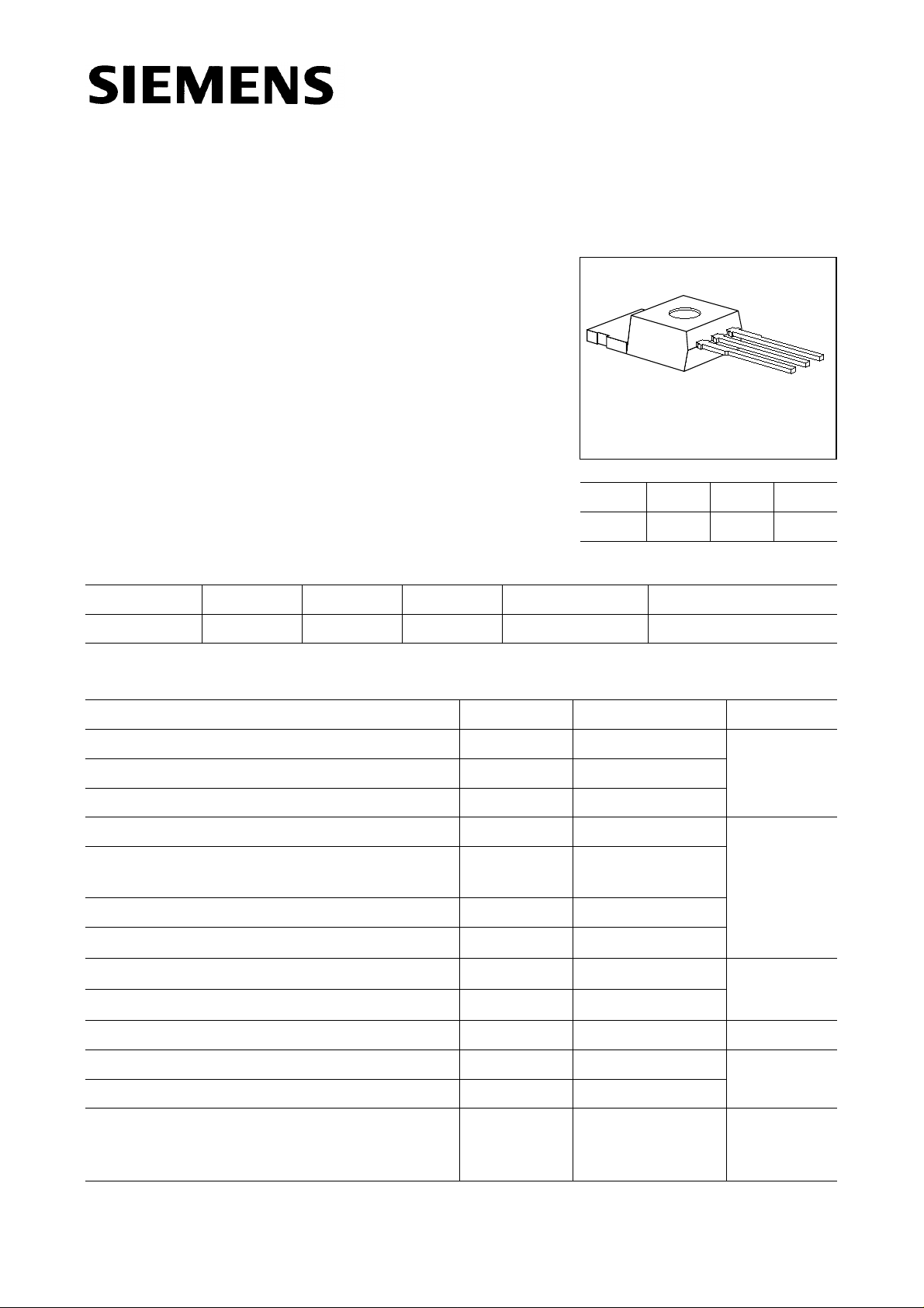
BTS 140A
Pin 1 2 3
GDS
3
2
1
Type
V
DS
I
D
R
DS(on)
Package Ordering Code
BTS 140A 50 V 42 A 0.028 Ω TO-220AB C67078-S5011-A2
Maximum Ratings
Parameter Symbol Values Unit
Drain-source voltage
Drain-gate voltage,
R
= 20 kΩ V
GS
Gate-source voltage
T
Continuous drain current,
= 65 °C I
C
ISO drain current
T
= 85° C, VGS = 10 V, VDS = 0.5 V
C
T
Pulsed drain current,
Short circuit current,
Short circuit dissipation,
= 25 °C I
C
T
= – 55 ... + 150 °C
j
T
= – 55 ... + 150 °C
j
Power dissipation
Operating and storage temperature range
V
DS
DGR
V
GS
D
I
D-ISO
D puls
I
SC
P
SCmax
P
tot
T
j
, T
stg
50 V
50
± 20
42 A
13.5
168
80
1200 W
125
– 55 ... + 150 °C
DIN humidity category, DIN 40 040 – E –
IEC climatic category, DIN IEC 68-1 – 55/150/56
Thermal resistance
Chip-case
Chip-ambient
R
R
th JC
th JA
≤ 1.0
≤ 75
K/W
Semiconductor Group 1 04.97
Page 2
BTS 140A
Electrical Characteristics
at Tj = 25 °C, unless otherwise specified.
Parameter Symbol Values Unit
min. typ. max.
Static Characteristics
Drain-source breakdown voltage
V
= 0, ID = 0.25 mA
GS
Gate threshold voltage
V
= V
, I
GS
DS
= 1 mA
D
Zero gate voltage drain current
V
= 0 V, VDS = 50 V
GS
T
= 25 °C
j
T
= 125 °C
j
Gate-source leakage current
V
= ± 20 V, VDS = 0
GS
T
= 25 °C
j
T
= 150 °C
j
Drain-source on-state resistance
V
= 10 V, ID =32 A
GS
Dynamic Characteristics
Forward transconductance
V
≥ 2 × ID× R
DS
DS(on)max
, ID = 32 A
Input capacitance
V
= 0, VDS = 25 V, f = 1 MHz
GS
Output capacitance
V
= 0, VDS = 25 V, f = 1 MHz
GS
Reverse transfer capacitance
V
= 0, VDS = 25 V, f = 1 MHz
GS
Turn-on time
V
= 25 V, VGS = 10 V, ID = 3 A, RGS = 50 Ω
CC
Turn-off time
V
= 25 V, VGS = 10 V, ID = 3 A, RGS = 50 Ω
CC
t
, (ton = t
on
t
, (t
off
off
= t
d(on)
d(off)
+ tr)
+ tf)
V
(BR)DSS
V
GS(th)
I
DSS
I
GSS
R
DS(on)
g
fs
C
iss
C
oss
C
rss
t
d(on)
t
r
t
d(off)
t
f
V
50 – –
2.5 3.0 3.5
µA
–
–
–
–
0.1
10
10
2.0
1.0
100
100
4.0
nA
µA
Ω
– 0.024 0.028
S
12 26 –
pF
– 1800 2400
– 800 1200
– 280 450
–3550ns
– 85 130
– 220 280
– 140 180
Semiconductor Group 2
Page 3
BTS 140A
Electrical Characteristics (cont’d)
at Tj = 25 °C, unless otherwise specified.
Parameter Symbol Values Unit
min. typ. max.
Reverse Diode
Continuous source current
Pulsed source current
Diode forward on-voltage
I
= 84 A, VGS = 0
F
Reverse recovery time
I
= IS, diF/dt = 100 A/µs, VR = 30 V
F
Reverse recovery charge
I
= I S, diF/dt = 100 A/µs, VR = 30 V
F
Temperature Sensor
Forward voltage
I
= 10 mA, Tj = – 55 ... + 150 °C
TS(on)
Sensor override, tp≤ 100 µs
T
= – 55 ... + 160 °C
j
Forward current
T
= – 55 ... + 150 °C
j
Sensor override, tp≤ 100 µs
T
= – 55 ... + 160 °C
j
V
Holding current,
= 5 V, Tj = 25 °C
TS(off)
Switching temperature
V
= 5 V
TS
Turn-off time
V
= 5 V, I
TS
TS(on)
= 2 mA
T
= 150 °C
j
I
S
I
SM
V
SD
t
rr
Q
V
TS(on)
I
TS(on)
I
H
T
TS(on)
t
off
– – 42 A
– – 168
V
– 1.8 2.2
ns
–80–
rr
µC
– 0.14 –
V
–
–
1.4
–
1.50
10
mA
–
–
0.05
0.05
–
–
0.1
0.2
5
600
0.5
0.3
°C
150 – –
µs
0.5 – 2.5
Semiconductor Group 3
Page 4

BTS 140A
Examples for short-circuit protection
at Tj = – 55 ... + 150 °C, unless otherwise specified.
Parameter Symbol Examples Unit
12–
Drain-source voltage
Gate-source voltage
Short-circuit current
Short-circuit dissipation
Response time
T
= 25 °C, before short circuit
j
Short-circuit protection ISC = f (VDS)
Parameter:V
GS
DiagramtodetermineISCforTj=– 55...+150°C
V
DS
V
GS
I
SC
P
SC
t
SC(off)
15 30 – V
6.2 5.0 –
≤ 80 ≤ 40 – A
≤ 1200 ≤ 1200 – W
≤ 20 ≤ 25 –
Max. gate voltage V
Parameter: Tj= – 55 ... + 150°C
GS(SC)
ms
= f (VDS)
Semiconductor Group 4
Page 5

BTS 140A
Max. power dissipation P
= f (TC)
tot
Typ. drain-source on-state resistance
R
= f (ID)
DS(on)
Parameter:V
GS
Typical output characteristics ID = f (VDS)
Parameter:tp =80µs
Safe operating area ID = f (VDS)
Parameter: D = 0.01, TC=25°C
Semiconductor Group 5
Page 6

BTS 140A
Drain-source on-state resistance
R
= f (Tj)
DS(on)
Parameter: ID= 32 A, VGS = 10 V (spread)
Gate threshold voltage V
GS(th)
Parameter:VDS = VGS, ID= 1 mA
= f (Tj)
Typ. transfer characteristic
I
= f (VGS)
D
Parameter:tp = 80 µs, VDS = 25 V
Typ. transconductance gfs = f (ID)
Parameter: tp = 80 µs, VDS = 25 V
Semiconductor Group 6
Page 7

BTS 140A
Continuous drain current ID= f (TC)
Parameter: VGS≥ 10 V
Forward characteristics of reverse diode
I
= f (VSD)
F
Parameter:Tj,tp = 80 µs (spread)
Typ. gate-source leakage current
I
= f (TC)
GSS
Parameter: VGS = 20 V, VDS = 0
Typ. capacitances C = f (VDS)
Parameter: VGS = 0, f = 1 MHz
Semiconductor Group 7
Page 8

BTS 140A
Transient thermal impedance Z
Parameter:D = tp/T
thJC
= f (tp)
Semiconductor Group 8
Page 9

TO 220 AB Ordering Code
Standard C67078-S5011-A2
9.9
2.8
9.5
3.7
4.4
1.3
BTS 140A
Package Outlines
17.5
1)
12.8
1
4.6
2)
0.75
1.05
2.542.54
1) punch direction, burr max. 0.04
2) dip tinning
3) max. 14.5 by dip tinning press burr max. 0.05
9.2
0.5
2.4
GPT05155
15.6
3)
13.5
Semiconductor Group 9
 Loading...