

Page 1
Philips Semiconductors Product specification
Breakover diodes BR211 series
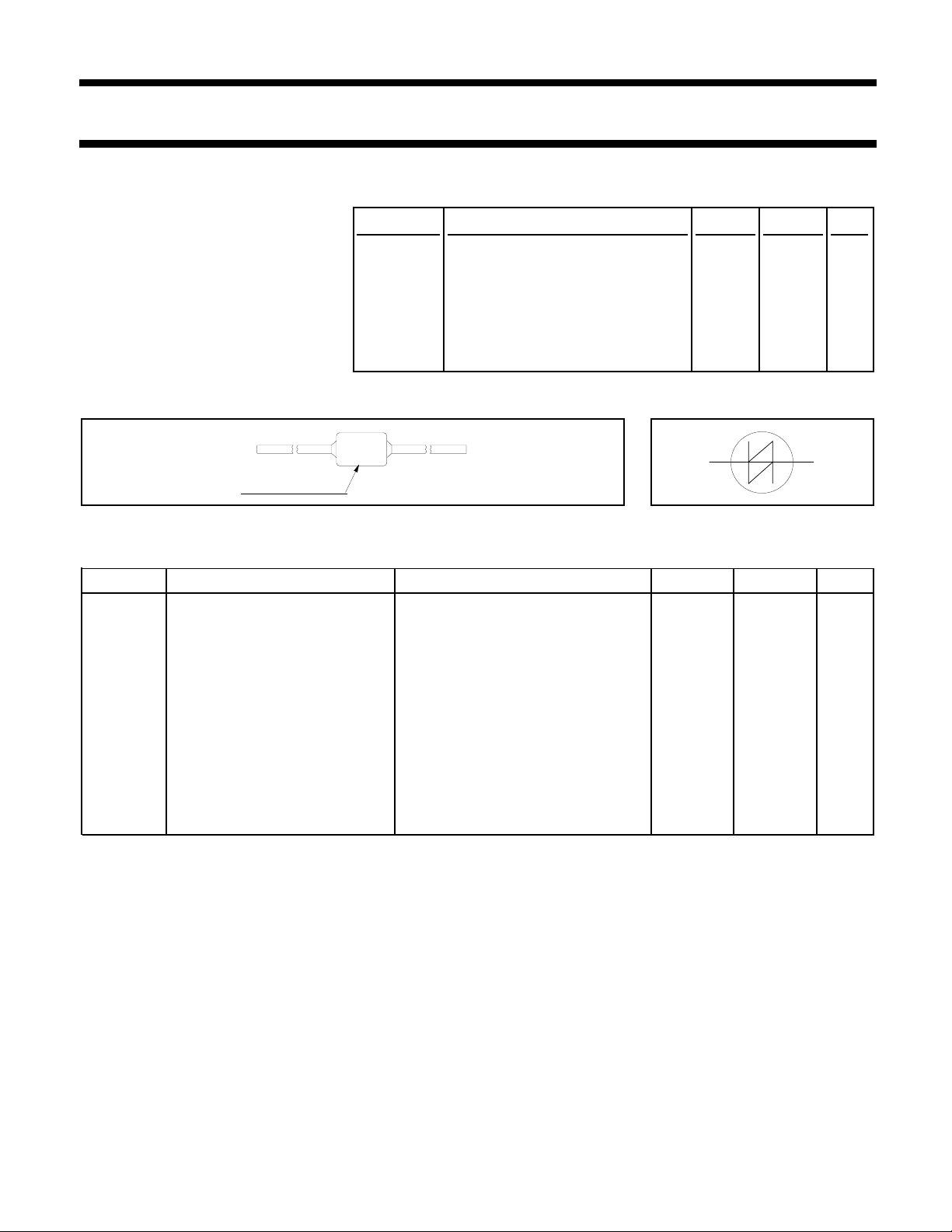
GENERAL DESCRIPTION QUICK REFERENCE DATA
A range of bidirectional, breakover SYMBOL PARAMETER MIN. MAX. UNIT
diodes in an axial, hermetically
sealed, glass envelope. These BR211-140 to 280
devicesfeature controlled breakover V
voltage and high holding current I
together with high peak current I
handling capability. Typical
(BO)
H
TSM
applications include transient
overvoltage protection in
telecommunications equipment.
OUTLINE - SOD84 SYMBOL
BR211-XXX
XXX denotes voltage grade
Breakover voltage 140 280 V
Holding current 150 - mA
Non-repetitive peak current - 40 A
LIMITING VALUES
Limiting values in accordance with the Absolute Maximum System (IEC 134).
SYMBOL PARAMETER CONDITIONS MIN. MAX. UNIT
V
D
I
TSM1
I
TSM2
I2tI
dIT/dt Rate of rise of on-state current tp = 10 µs - 50 A/µs
P
tot
P
TM
T
stg
T
a
T
vj
Continuous voltage - 75% of V
V
Non repetitive peak current 10/320 µs impulse equivalent to - 40 A
(BO)typ
10/700 µs, 1.6 kV voltage impulse
(CCITT K17)
Non repetitive on-state current half sine wave; t = 10 ms; - 15 A
2
t for fusing tp = 10 ms - 1.1 A2s
after V
turn-on
(BO)
Tj = 70 ˚C prior to surge
Continuous dissipation Ta = 25˚C - 1.2 W
Peak dissipation tp = 1 ms; Ta = 25˚C - 50 W
Storage temperature -65 150 ˚C
Operating ambient temperature off-state - 70 ˚C
Overload junction temperature on-state - 150 ˚C
August 1996 1 Rev 1.200
Page 2

Philips Semiconductors Product specification
Breakover diodes BR211 series
THERMAL RESISTANCES
SYMBOL PARAMETER CONDITIONS MIN. TYP. MAX. UNIT
R
th j-e
R
th j-a
Z
th j-a
R
th e-tp
R
th e-a
R
th tp-a
STATIC CHARACTERISTICS
Tj = 25 ˚C unless otherwise stated
SYMBOL PARAMETER CONDITIONS MIN. TYP. MAX. UNIT
1
V
TM
V
(BR)
V
(BO)
S
(br)
2
I
H
3
I
S
4
I
D
Thermal resistance junction to - 22 - K/W
envelope
Thermal resistance junction to mounted as fig:12 - 105 K/W
ambient
Thermal impedance junction to tp = 1 ms - 2.62 - K/W
ambient
Thermal resistance envelope to lead length = 5 mm - 15 - K/W
tie point lead length = 10 mm - 30 - K/W
Thermal resistance envelope to lead length = 5 mm - 440 - K/W
ambient lead length = 10 mm - 350 - K/W
Thermal resistance tie point to mounted as fig:12 - 70 - K/W
ambient mounted with 1 cm2 copper - 55 - K/W
laminate per lead.
mounted with 2.25 cm2 copper - 45 - K/W
laminate per lead
On-state voltage ITM = 2 A - - 2.5 V
Avalanche voltage (min) I
Breakover voltage (max) I ≤ IS, tp = 100 µs
(BR)
= 10
mA
BR211-140 123 140 157 V
BR211-160 140 160 180 V
BR211-180 158 180 202 V
BR211-200 176 200 224 V
BR211-220 193 220 247 V
BR211-240 211 240 269 V
BR211-260 228 260 292 V
BR211-280 246 280 314 V
V
V
Temperature coefficient of V
Holding current Tj = 25˚C 150 - - mA
(BR)
- +0.1 - %/K
Tj = 70˚C 100 - - mA
Switching current tp = 100 µs 10 200 1000 mA
Off-state current VD = 85% V
, Tj = 70˚C - - 10 µA
(BR)min
1 Measured under pulsed conditions to avoid excessive dissipation
2 The minimum current at which the diode will remain in the on-state
3 The avalanche current required to switch the diode to the on-state
4 Measured at maximum recommended continuous voltage. Illuminance ≤ 500 lux (daylight); relative
humidity < 65%.
August 1996 2 Rev 1.200
Page 3
Philips Semiconductors Product specification
Breakover diodes BR211 series
DYNAMIC CHARACTERISTICS
Tj = 25 ˚C unless otherwise stated
SYMBOL PARAMETER CONDITIONS MIN. TYP. MAX. UNIT
dVD/dt Linear rate of rise of off-state V
voltage that will not trigger any
device
C
j
Off-state capacitance VD = 0 V; f = 1 kHz to 1 MHz - - 100 pF
= 85% V
(DM)
; Tj = 70 ˚C - - 2000 V/µs
(BR)min
IT
IH
VT
V(BR)
I(BR)
ID
VD
Symbol
Symmetric BOD
IS
V(BO)
voltage
current
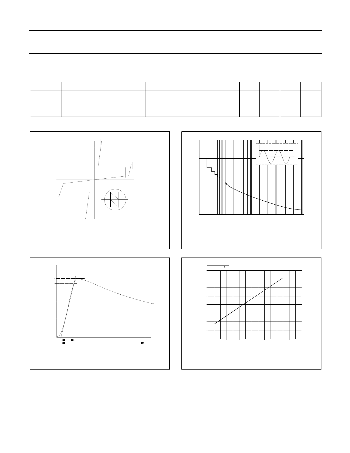
Fig.1. Definition of breakover diode characteristics
current
100%
90%
50%
30%
0
10us
Fig.2. Test waveform for high voltage impulse (I
according to CCITT vol IX-Rec K17.
ITSM
time
700us
TSM1
ITSM / A
20
15
10
5
0
1 10 100 1000 10000
.
Fig.3. Maximum permissible non-repetitive on-state
BR211
I
Number of impulses
ITSM2
time
current based on sinusoidal currents; f = 50 Hz;
device triggered at the start of each pulse; Tj = 70˚C
prior to surge.
V(BR)(Tj)
V(BR)(25 C)
1.06
1.04
1.02
1.00
0.98
0.96
0.94
0.92
0.90
)
Fig.4. Normalised avalanche breakdown voltage V
and V
-20 0 20 40 60 80 100
-40
as a function of temperature.
(BO)
Tj / C
(BR)
August 1996 3 Rev 1.200
Page 4
Philips Semiconductors Product specification
Breakover diodes BR211 series
IT / A
20
Tj = 25 C
Tj = 150 C
15
10
5
0
123
typ
VT / V
max
4
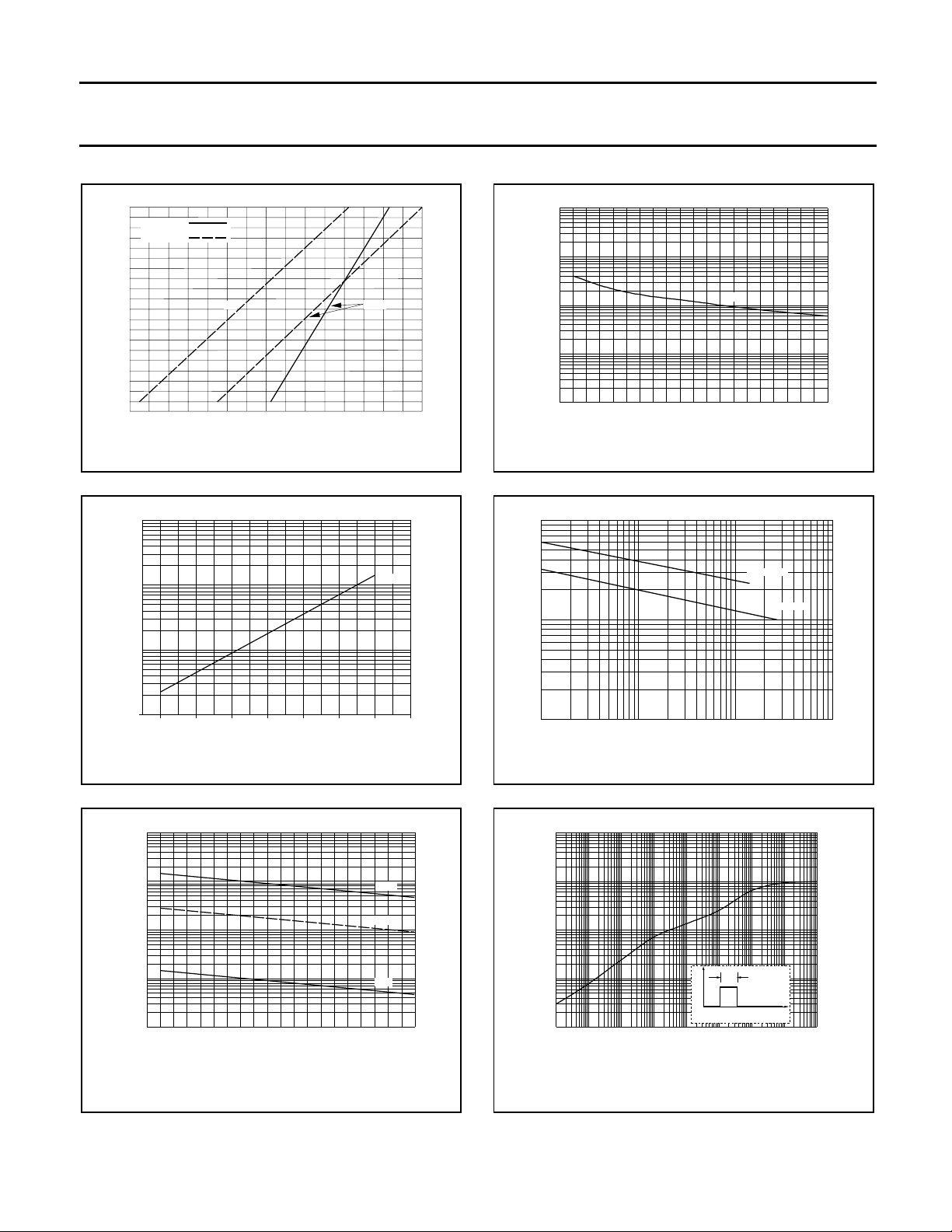
Fig.5. On-state current as a function of on-state
voltage; tp = 200 µs to avoid excessive dissipation.
ID / uA
100
10
1
max
IH / A
10
1
0.1
0.01
0.001
-50 0
min
50 150
Tj / C
100
Fig.8. Minimum holding current as a function of
temperature.
Cj / pF
100
typ
10
BR211-140
BR211-280
0.1
-20 0 20 40 60 80 100
-40
Tj / C
Fig.6. Maximum off-state current as a function of
temperature.
IS / A
10
1
0.1
0.01
0.001
-50 0
50 150
Tj / C
max
typ
min
100
Fig.7. Switching current as a function of junction
temperature.
1
1 10 100
VD / V
1000
Fig.9. Typical junction capacitance as a function of
off-state voltage, f = 1 MHz; Tj = 25˚C.
Zth / (K/W)
1000
100
10
t
P
1
0.1
10us 1ms
0.1s 10s 1000s
tp / s
p
D
Fig.10. Transient thermal impedance. Zth
BR211
t
= f(tp).
j-a
August 1996 4 Rev 1.200
Page 5
Philips Semiconductors Product specification
Breakover diodes BR211 series
Rth e-tp
tie-point
Rth tp-a
junction
Rth j-e
ambient
envelope
Rth e-a
50
3
50
72
25
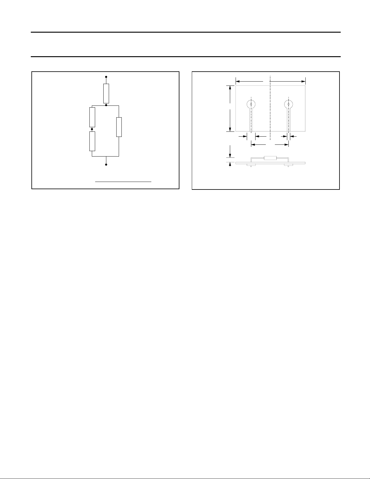
Fig.11. Components of thermal resistance, Fig.12. Mounting on pcb used for Rth measurement.
Rthj − a = Rthj −e +
Rthe −a.(Rthe −tp +Rthtp −a)
(Rthe −a + Rthe − tp +Rthtp −a)
August 1996 5 Rev 1.200
Page 6
Philips Semiconductors Product specification
Breakover diodes BR211 series
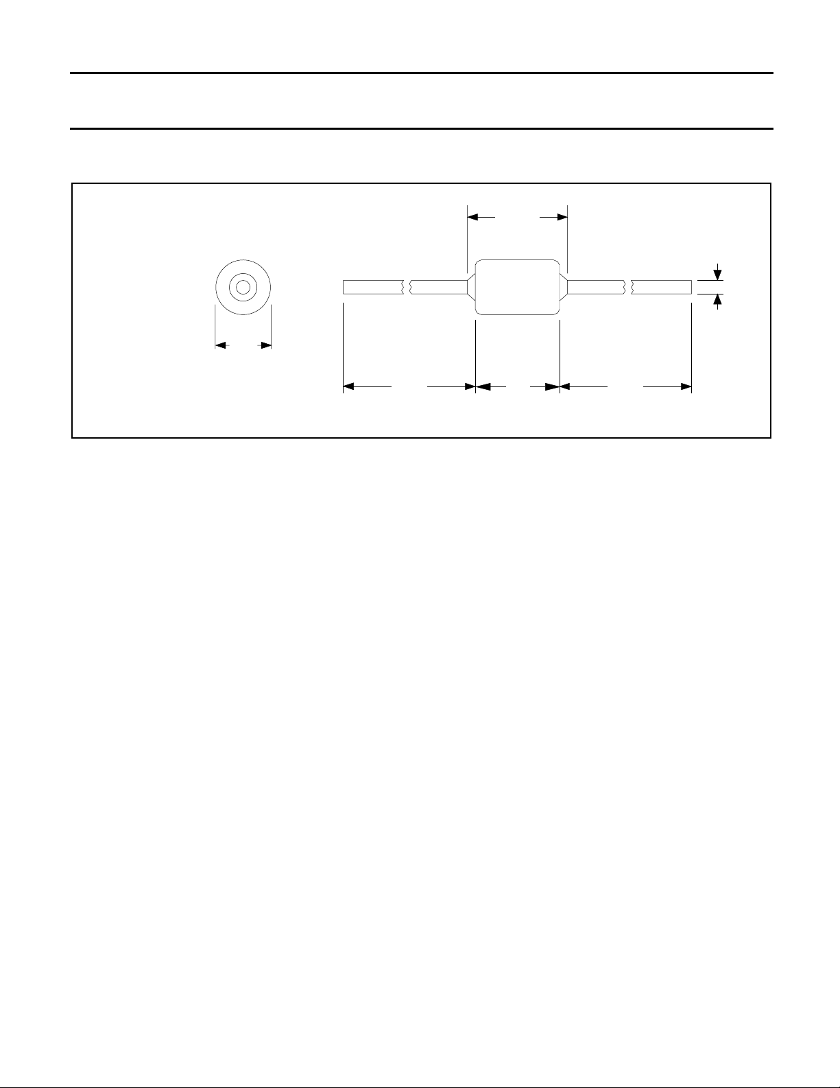
MECHANICAL DATA
Dimensions in mm
3.15
max
28
min
5
max
4.3
max
Fig.13. SOD84.
0.81
max
28
min
August 1996 6 Rev 1.200
Page 7

Philips Semiconductors Product specification
Breakover diodes BR211 series
DEFINITIONS
Data sheet status
Objective specification This data sheet contains target or goal specifications for product development.
Preliminary specification This data sheet contains preliminary data; supplementary data may be published later.
Product specification This data sheet contains final product specifications.
Limiting values
Limiting values are given in accordance with the Absolute Maximum Rating System (IEC 134). Stress above one
or more of the limiting values may cause permanent damage to the device. These are stress ratings only and
operation of the device at these or at any other conditions above those given in the Characteristics sections of
this specification is not implied. Exposure to limiting values for extended periods may affect device reliability.
Application information
Where application information is given, it is advisory and does not form part of the specification.
Philips Electronics N.V. 1996
All rights are reserved. Reproduction in whole or in part is prohibited without the prior written consent of the
copyright owner.
The information presented in this document does not form part of any quotation or contract, it is believed to be
accurate and reliable and may be changed without notice. No liability will be accepted by the publisher for any
consequence of its use. Publication thereof does not convey nor imply any license under patent or other
industrial or intellectual property rights.
LIFE SUPPORT APPLICATIONS
These products are not designed for use in life support appliances, devices or systems where malfunction of these
products can be reasonably expected to result in personal injury. Philips customers using or selling these products
for use in such applications do so at their own risk and agree to fully indemnify Philips for any damages resulting
from such improper use or sale.
August 1996 7 Rev 1.200
 Loading...