

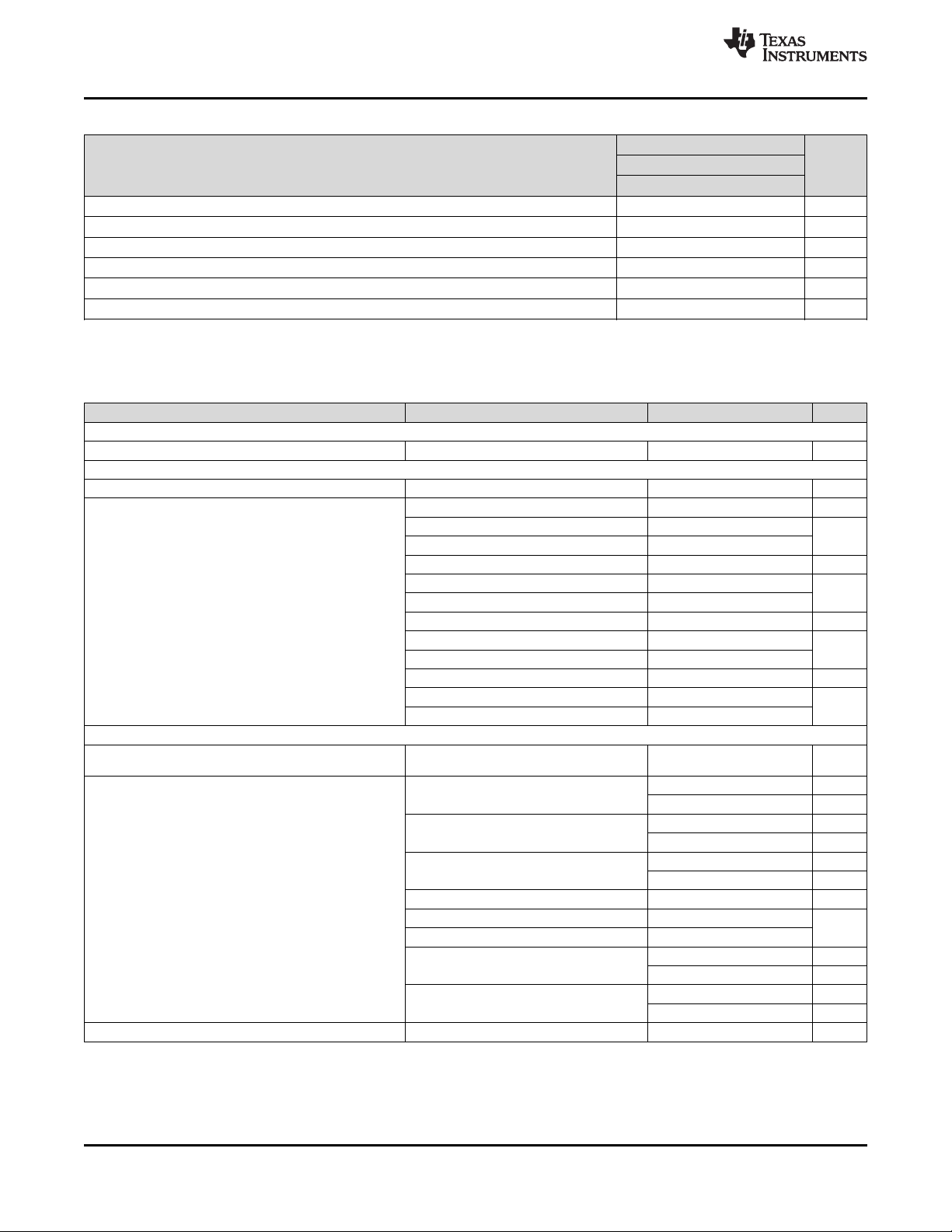
Page 1
R
SR
Adapter
4.5-24V
HOST
bq24780S
Hybrid Power
Boost Charge
Controller
SYS
Battery
Pack
N-FET Driver
N-FET Driver
1S-4S
SMBus
IADP, ,PROCHOT
PMON, IDCHG
SMBus Controls V & I
with high accuracy
Adapter Detection
Enhanced Safety:
OCP,OVP, FET Short
Integration:
Loop Compensation; Soft-Start
Comparator, BTST Diode
R
AC
Product
Folder
Order
Now
Technical
Documents
Tools &
Software
Support &
Community
bq24780S
SLUSC27C –APRIL 2015–REVISED MARCH 2017
bq24780S 1- to 4-Cell Hybrid Power Boost Mode Battery Charge Controller
With Power and Processor Hot Monitoring
1 Features
1
• Industrial Innovative Charge Controller With
Hybrid Power Boost Mode
– Adapter and Battery Provides Power to
System Together for Intel®CPU Turbo Mode
– Ultra-Fast Transient Response of 150 µs to
Enter Boost Mode
– Hybrid Power Boost Mode from 4.5- to 24-V
System
– Charge 1- to 4-Cell Battery Pack from 4.5- to
24-V Adapter
• High Accuracy Power and Current Monitoring for
CPU Throttling
– Comprehensive PROCHOT Profile
– ± 2% Current Monitor Accuracy
– ± 5% System Power Monitor Accuracy
(PMON)
• Automatic NMOS Power Source Selection from
Adapter or Battery
– ACFET Fast Turn on in 100 µs
• Programmable Input Current, Charge Voltage,
Charge and Discharge Current Limit
– ±0.4% Charge Voltage (16-mV step)
– ±2% Input Current (128-mA/step)
– ±2% Charge Current (64-mA/step)
– ±2% Discharge Current (512-mA/step)
• High Integration
– Battery LEARN Function
– Battery Present Monitor
– Boost Mode Indicator
– Loop Compensation
– BTST Diode
• Enhanced Safety Features for Overvoltage
Protection, Overcurrent Protection, Battery,
Inductor, and MOSFET Short-Circuit Protection
• Switching Frequency: 600 kHz, 800 kHz, and
1 MHz
• Realtime System Control on ILIM Pin to Limit
Charge and Discharge Current
• 0.65 mA Adapter Standby Quiescent Current for
Energy Star
1
An IMPORTANT NOTICE at the end of this data sheet addresses availability, warranty, changes, use in safety-critical applications,
intellectual property matters and other important disclaimers. PRODUCTION DATA.
2 Applications
• Notebook, Ultrabook, Detachable, and Tablet PC
• Handheld Terminal
• Industrial and Medical Equipment
• Portable Equipment
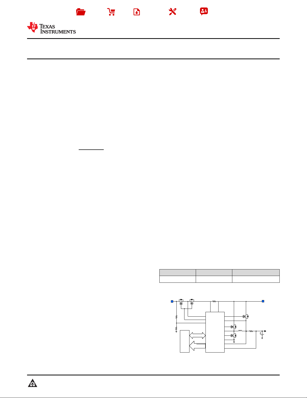
3 Description
The bq24780S device is a high-efficiency,
synchronous battery charger, offering low component
count for space-constrained, multi-chemistry battery
charging applications.
The bq24780S device supports hybrid power boost
mode (previously called "turbo boost mode"). It allows
battery discharge energy to system when system
power demand is temporarily higher than adapter
maximum power level. Therefore, adapter does not
crash.
The bq24780S device uses two charge pumps to
separately drive N-channel MOSFETs (ACFET,
RBFET, and BATFET) for automatic system power
source selection.
Through SMBus, system power management
microcontroller programs input current, charge
current, discharge current, and charge voltage DACs
with high regulation accuracies.
The bq24780S device monitors adapter current
(IADP), battery discharge current (IDCHG), and
system power (PMON) for host to throttle back CPU
speed or reduce system power when needed.
The bq24780S device charges 1-, 2-, 3-, or 4-series
Li+ cells.
Device Information
PART NUMBER PACKAGE BODY SIZE (NOM)
bq24780S WQFN (28) 4.00 × 4.00 mm
(1) For all available packages, see the orderable addendum at
the end of the data sheet.
(1)
2
Page 2

bq24780S
SLUSC27C –APRIL 2015–REVISED MARCH 2017
www.ti.com
Table of Contents
1 Features.................................................................. 1
2 Applications ........................................................... 1
3 Description ............................................................. 1
4 Revision History..................................................... 2
5 Pin Configuration and Functions......................... 3
6 Specifications......................................................... 5
6.1 Absolute Maximum Ratings ...................................... 5
6.2 ESD Ratings.............................................................. 5
6.3 Recommended Operating Conditions....................... 5
6.4 Thermal Information.................................................. 6
6.5 Electrical Characteristics........................................... 6
6.6 Timing Requirements.............................................. 11
6.7 Typical Characteristics............................................ 13
7 Detailed Description............................................ 14
7.1 Overview ................................................................. 14
7.2 Functional Block Diagram ....................................... 15
7.3 Feature Description................................................. 16
7.4 Device Functional Modes........................................ 22
7.5 Programming........................................................... 23
7.6 Register Maps......................................................... 25
8 Application and Implementation ........................ 36
8.1 Application Information............................................ 36
8.2 Typical Applications ................................................ 36
9 Power Supply Recommendations...................... 44
10 Layout................................................................... 44
10.1 Layout Guidelines ................................................. 44
10.2 Layout Examples................................................... 45
11 Device and Documentation Support................. 48
11.1 Receiving Notification of Documentation Updates 48
11.2 Community Resources.......................................... 48
11.3 Trademarks........................................................... 48
11.4 Electrostatic Discharge Caution............................ 48
11.5 Glossary................................................................ 48
12 Mechanical, Packaging, and Orderable
Information........................................................... 48
4 Revision History
Changes from Revision B (April 2015) to Revision C Page
• Full data sheet to product folder............................................................................................................................................. 1
Changes from Revision A (April 2015) to Revision B Page
• Changed the Description for pin 22 (GND) in the Pin Functions table................................................................................... 4
• Changed the Thermal Pad to PowerPAD in the Pin Functions table..................................................................................... 4
• Changed 16X to 20X on the SRP and SRN pins of the Functional Block Diagram ............................................................ 15
• Changed C4 From: 0.01 μF To: 0.1 μF in Figure 17 ........................................................................................................... 36
Changes from Original (April 2015) to Revision A Page
• Changed V
in the Electrical Characteristics, MIN From: 190% To: 180%, MAX From: 215% To: 220% ..................... 9
(ACOC)
• Changed "ChargeOption() bit [0] = 0" To: REG0x12[0] in Enable and Disable Charging.................................................... 17
• Changed " (REG0x12[1])" To: (REG0x12[0]=1) in Enable and Disable Charging ............................................................... 17
• Changed " REG0x12" To: "REG0x12[0]" in Battery Charging ............................................................................................ 22
• Changed Bit [10:9] in Table 9 From: 11: 8 ms To: 11: 800 µs ............................................................................................ 30
• Added sentence to Bit [7:6] in Table 9 " If REG0x15() is programmed..." ........................................................................... 30
• Changed text in Bit [5] of Table 9 From: "write 0x3C[2] = 1." To: "write 0x3C[2] = 0."........................................................ 30
• Deleted text from Bit [5] of Table 9 "This function is not available in 1s battery."................................................................ 30
2
Submit Documentation Feedback Copyright © 2015–2017, Texas Instruments Incorporated
Page 3
Thermal
Pad
28 VCC8IDCHG
1ACN 21 ILIM
27 PHASE9PMON
2ACP 20 SRP
26 HIDRV10PROCHOT
3CMSRC 19 SRN
25 BTST11SDA
4ACDRV 18 BATDRV
24 REGN12SCL
5ACOK 17 BATSRC
23 LODRV13CMPIN
6ACDET 16 TB_STAT
22 GND14CMPOUT
7IADP 15 BATPRES
www.ti.com
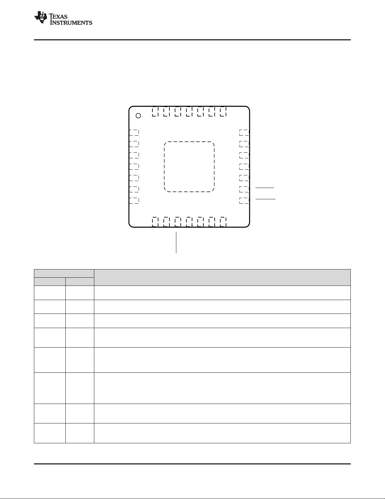
5 Pin Configuration and Functions
bq24780S
SLUSC27C –APRIL 2015–REVISED MARCH 2017
RUY Package
28-Pin WQFN
Top View
PIN
NAME NUMBER
ACN 1
ACP 2
CMSRC 3
Input current sense resistor negative input. Place an optional 0.01-µF ceramic capacitor from ACN to GND for
common-mode filtering. Place a 0.1-µF ceramic capacitor from ACN to ACP to provide differential mode filtering.
Input current sense resistor positive input. Place a 0.1-µF ceramic capacitor from ACP to GND for commonmode filtering. Place a 0.1-µF ceramic capacitor from ACN to ACP to provide differential-mode filtering.
ACDRV charge pump source input. Place a 4-kΩ resistor from CMSRC to the common source of ACFET (Q1)
and RBFET (Q2) to limit the inrush current on CMSRC pin.
Charge pump output to drive both adapter input N-channel MOSFET (ACFET) and reverse blocking N-channel
ACDRV 4
MOSFET (RBFET). ACDRV voltage is 6 V above CMSRC when ACOK is HIGH. Place a 4-kΩ resistor from
ACDRV to the gate of ACFET and RBFET limits the inrush current on ACDRV pin.
Active HIGH AC adapter detection open drain output. It is pulled HIGH to external pullup supply rail by external
ACOK 5
ACDET 6
IADP 7
IDCHG 8
pullup resistor when a valid adapter is present (ACDET above 2.4 V, VCC above UVLO but below ACOV and
VCC above BAT). If any of the above conditions is not valid, ACOK is pulled LOW by internal MOSFET. Connect
a 10-kΩ pullup resistor from ACOK to the pullup supply rail.
Adapter detection input. Program adapter valid input threshold by connecting a resistor divider from adapter
input to ACDET pin to GND pin. When ACDET pin is above 0.6 V and VCC is above UVLO, REGN LDO is
present, ACOK comparator, input current buffer (IADP), discharge current buffer (IDCHG), independent
comparator, and power monitor buffer (PMON) can be enabled with SMBus. When ACDET is above 2.4V, and
VCC is above SRN but below ACOV, ACOK goes HIGH.
Buffered adapter current output. V
The ratio of 20x and 40x is selectable with SMBus. Place 100-pF (or less) ceramic decoupling capacitor from
IADP pin to GND. This pin can be floating if this output is not in use.
Buffered discharge current. V
The ratio of 8x or 16x is selectable with SMBus. Place 100-pF (or less) ceramic decoupling capacitor from
IDSCHG pin to GND. This pin can be floating if this output is not in use.
Pin Functions
= 20 or 40 × (V
(IADP)
= 8 or 16 × (V
(IDCHG)
DESCRIPTION
– V
(ACP)
– V
(SRN)
(SRP)
(ACN)
)
)
Submit Documentation FeedbackCopyright © 2015–2017, Texas Instruments Incorporated
3
Page 4
bq24780S
SLUSC27C –APRIL 2015–REVISED MARCH 2017
Pin Functions (continued)
PIN
NAME NUMBER
Buffered total system power. The output current is proportional to the total power from the adapter and battery.
PMON 9
The ratio is selectable through SMBus. Place a resistor from PMON pin to GND to generate PMON voltage.
Place a 100-pF (or less) ceramic decoupling capacitor from PMON pin to GND. This pin can be floating if this
output is not in use.
Active low, open-drain output of the processor hot indicator. The charger IC monitors events like adapter current,
PROCHOT 10
battery discharge current. After any event in the PROCHOT profile is triggered, a minimum 10-ms pulse is
asserted.
SMBus open-drain data I/O. Connect to SMBus data line from the host controller or smart battery. SMBus
SDA 11
communication starts when VCC is above UVLO. Connect a 10-kΩ pullup resistor according to SMBus
specifications.
SMBus open-drain clock input. Connect to SMBus clock line from the host controller or smart battery. SMBus
SCL 12
communication starts when VCC is above UVLO. Connect a 10-kΩ pullup resistor according to SMBus
specifications.
Input of independent comparator. Internal reference, output polarity and deglitch time is selectable by SMBus.
CMPIN 13
Place a resistor between CMPIN and CMPOUT to program hysteresis when the polarity is HIGH. If comparator
is not in use, CMPIN is tied to ground, and CMPOUT is left floating.
Open-drain output of independent comparator. Place 10-kΩ pullup resistor from CMPOUT to pullup supply rail.
CMPOUT 14
Comparator reference, output polarity and deglitch time is selectable by SMBus. If comparator is not in use,
CMPIN is tied to ground, and CMPOUT is left floating.
Active low battery present input signal. Low indicates battery present, high indicates battery absent. The device
BATPRES 15
exits the LEARN function and turns on ACFET/RBFET within 100 µs if BATPRES pin is pulled high. Upon
BATPRES from LOW to HIGH, battery charging and hybrid power boost mode are disabled. The host can
enable charging and hybrid power boost mode by write to REG0x14() and REG0x15() when BATPRES is HIGH
Active low, open-drain output for hybrid power boost mode indication. It is pulled low when the IC is operating in
TB_STAT 16
boost mode. Otherwise, it is pulled high. Connect a 10-kΩ pullup resistor from TB_STAT pin to the pullup supply
rail.
BATSRC 17 Connect to the source of N-channel BATFET. BATDRV voltage is 6 V above BATSRC to turn on BATFET.
Charge pump output to drive N-channel MOSFET between battery and system (BATFET). BATDRV voltage is
BATDRV 18
6 V above BATSRC to turn on BATFET and power system from battery. BATDRV is shorted to BATSRC to turn
off BATFET. Place a 4-kΩ resistor from BATDRV to the gate of BATFET limits the inrush current on BATDRV
pin.
Charge current sense resistor negative input. SRN pin is for battery voltage sensing as well. Connect SRN pin
SRN 19
with a 0.1-µF ceramic capacitor to GND for common-mode filtering. Connect a 0.1-µF ceramic capacitor from
SRP to SRN to provide differential mode filtering.
SRP 20
Charge current sense resistor positive input. Connect a 0.1-µF ceramic capacitor from SRP to SRN to provide
differential mode filtering.
Charge current and discharge current limit.V
V
) for discharge current. Program ILIM voltage by connecting a resistor divider from system reference 3.3-V
ILIM 21
SRP
rail to ILIM pin to GND pin. The lower of ILIM voltage and 0x14() (for charge) or 0x39 (for discharge) reference
sets actual regulation limit. The minimum voltage on ILIM to enable charge or discharge current regulation is 120
mV.
GND 22
IC ground. On PCB layout, connect to analog ground plane, and only connect to power ground plan through pad
underneath IC.
LODRV 23 Low-side power MOSFET driver output. Connect to low-side N-channel MOSFET gate.
6-V linear regulator output supplied from VCC. The LDO is active when ACDET above 0.6 V, VCC above UVLO.
REGN 24
Connect a ≥ 2.2-µF 0603 ceramic capacitor from REGN to GND. The diode between REGN and BTST is
integrated.
BTST 25
High-side power MOSFET driver power supply. Connect a 47-nF capacitor from BTST to PHASE. The diode
between REGN and BTST is integrated inside the IC.
HIDRV 26 High-side power MOSFET driver output. Connect to the high side N-channel MOSFET gate.
PHASE 27 High-side power MOSFET driver source. Connect to the source of the high-side N-channel MOSFET.
VCC 28
Input supply from adapter or battery. Use 10-Ω resistor and 1-µF capacitor to ground as a low pass filter to limit
inrush current. A diode OR is connected to VCC. It powers charger IC from input adapter and battery.
Exposed pad beneath the IC. Analog ground and power ground star-connected only at the PowerPAD plane.
PowerPAD™
Always solder the PowerPAD to the board and have vias on the PowerPAD plane connecting to analog ground
and power ground planes. It also serves as a thermal pad to dissipate the heat.
DESCRIPTION
= 20 × (V
ILIM
SRP
– V
) for charge current and V
SRN
ILIM
= 5 × (V
www.ti.com
SRN
–
4
Submit Documentation Feedback Copyright © 2015–2017, Texas Instruments Incorporated
Page 5
bq24780S
www.ti.com
SLUSC27C –APRIL 2015–REVISED MARCH 2017
6 Specifications
6.1 Absolute Maximum Ratings
over operating free-air temperature range (unless otherwise noted)
SRN, SRP, ACN, ACP, CMSRC, VCC, BATSRC –0.3 30
PHASE –2 30
Voltage
Differential voltage BTST-PHASE, HIDRV-PHASE ACDRV-CMSRC, BATDRV-BATSRC –0.3 7 V
Voltage
Voltage PHASE (2% duty cycle) –4 30 V
Voltage REGN (5ms) –0.3 9 V
Maximum differential voltage SRP–SRN, ACP–ACN –0.5 +0.5 V
Junction temperature, T
Storage temperature, T
J
stg
(1) Stresses beyond those listed under absolute maximum ratings may cause permanent damage to the device. These are stress ratings
only, and functional operation of the device at these or any other conditions beyond those indicated under recommended operating
conditions is not implied. Exposure to absolute-maximum-rated conditions for extended periods may affect device reliability.
(2) All voltages are with respect to GND if not specified. Currents are positive into, negative out of the specified pin. Consult Packaging
Section of the data book for thermal limitations and considerations of packages.
ACDET, SDA, SCL, LODRV, REGN, IADP, IDCHG, PMON, ILIM, ACOK,
CMPIN, CMPOUT, BATPRES, TB_STAT
PROCHOT –0.3 5.7
BTST, HIDRV, ACDRV, BATDRV –0.3 36
LODRV (2% duty cycle) –4 7
HIDRV (2% duty cycle) –4 36
(1)(2)
MIN MAX UNIT
–0.3 7
–40 155 °C
–55 155 °C
V
V
6.2 ESD Ratings
VALUE UNIT
(1)
±2000
±500
V
(ESD)
Electrostatic discharge
Human body model (HBM), per ANSI/ESDA/JEDEC JS-001
Charged device model (CDM), per JEDEC specification JESD22-
(2)
C101
(1) JEDEC document JEP155 states that 500-V HBM allows safe manufacturing with a standard ESD control process.
(2) JEDEC document JEP157 states that 250-V CDM allows safe manufacturing with a standard ESD control process.
6.3 Recommended Operating Conditions
over operating free-air temperature range (unless otherwise noted)
MIN MAX UNIT
SRN, SRP, ACN, ACP, CMSRC, VCC, BATSRC 0 24
PHASE –2 24
Voltage
Maximum difference SRP–SRN, ACP–ACN –0.4 +0.4 V
Junction temperature, T
Operating free-air temperature, T
ACDET, SDA, SCL, LODRV, REGN, IADP, IDCHG, PMON, ILIM, ACOK,
CMPIN, CMPOUT, BATPRES, TB_STAT
PROCHOT –0.3 5
BTST, HIDRV, ACDRV, BATDRV 0 30
J
A
0 6.5
–20 125
–40 85
V
V
°C
Submit Documentation FeedbackCopyright © 2015–2017, Texas Instruments Incorporated
5
Page 6
bq24780S
SLUSC27C –APRIL 2015–REVISED MARCH 2017
www.ti.com
6.4 Thermal Information
bq24780S
THERMAL METRIC
(1)
UNITRUY (WQFN)
28 PINS
R
R
R
ψ
ψ
R
θJA
θJCtop
θJB
JT
JB
θJCbot
Junction-to-ambient thermal resistance 33.3 °C/W
Junction-to-case (top) thermal resistance 29.7 °C/W
Junction-to-board thermal resistance 6.5 °C/W
Junction-to-top characterization parameter 0.3 °C/W
Junction-to-board characterization parameter 6.5 °C/W
Junction-to-case (bottom) thermal resistance 1.3 °C/W
(1) For more information about traditional and new thermal metrics, see the IC Package Thermal Metrics application report, SPRA953.
6.5 Electrical Characteristics
4.5 V ≤ V
OPERATING CONDITIONS
V
VCC(OP)
CHARGE VOLTAGE REGULATION
V
BAT(REG_RNG)
V
BAT(REG_ACC)
CHARGE CURRENT REGULATION
V
IREG(CHG_RNG)
I
CHRG(REG_ACC)
I
LGK(SRP-SRN)
≤ 24 V, –40°C ≤ TJ≤ 125°C, typical values are at TA= 25°C, with respect to GND (unless otherwise noted)
VCC
PARAMETER TEST CONDITIONS MIN TYP MAX UNIT
VCC/ACP/ACN operating voltage 4.5 24 V
Battery voltage 1.024 19.2 V
ChargeVoltage() = 0x41A0 16.8 V
–10°C-85°C –0.4% 0.4%
–40°C-125°C –0.5% 0.5%
ChargeVoltage() = 0x3130 12.592 V
–10°C-85°C –0.4% 0.4%
Charge voltage regulation accuracy
Charge current regulation differential
voltage
Charge current regulation accuracy
(SRN > 2.8 V)
SRP and SRN leakage mismatch –8 8 µA
–40°C-125°C –0.5% 0.5%
ChargeVoltage() = 0x20D0 8.4 V
–10°C-85°C –0.4% 0.4%
–40°C-125°C –0.6% 0.6%
ChargeVoltage() = 0x1060 4.192 V
–10°C-85°C –0.5% 0.8%
–40°C-125°C –0.7% 0.8%
V
ChargeCurrent() = 0x1000
ChargeCurrent() = 0x0800
ChargeCurrent() = 0x0200
ChargeCurrent() = 0x0100 256 mA
ChargeVoltage() = 0x20D0, 0x3031, 0x41A0 –16% 16%
ChargeVoltage() = 0x1060 –20% 20%
ChargeCurrent() = 0x00C0
ChargeCurrent() = 0x0080
IREG(CHG)
= V
SRP
– V
SRN
0 81.28 mV
4096 mA
–2% 2%
2048 mA
–3% 3%
512 mA
–10% 10%
192 mA
–20% 20%
128 mA
–30% 30%
6
Submit Documentation Feedback Copyright © 2015–2017, Texas Instruments Incorporated
Page 7
www.ti.com
Electrical Characteristics (continued)
bq24780S
SLUSC27C –APRIL 2015–REVISED MARCH 2017
4.5 V ≤ V
≤ 24 V, –40°C ≤ TJ≤ 125°C, typical values are at TA= 25°C, with respect to GND (unless otherwise noted)
VCC
PARAMETER TEST CONDITIONS MIN TYP MAX UNIT
DISCHARGE CURRENT REGULATION
V
(IREG_CHG_RNG)
I
(DCHRG_REG_ACC)
Charge current regulation differential
voltage
Discharge current regulation accuracy
INPUT CURRENT REGULATION
V
(IREG_DPM_RNG)
I
(DPM_REG_ACC)
I
LGK(ACP-ARN)
Input current regulation differential
voltage
Input current regulation accuracy
ACP and ACN leakage mismatch –5 5 µA
INPUT CURRENT SENSE AMPLIFIER
V
(IADP)
I
(IADP)
A
(IADP)
V
(IADP_ACC)
V
(IADP_CLAMP)
C
(IADP)
IADP output voltage 0 3.3 V
IADPT output current 0 1 mA
IADP sense amplifier gain V
Current sense amplifier gain accuracy
IADP clamp voltage 3 3.3 V
IADP output load capacitance With 0 to 1mA load 100 pF
DISCHARGE CURRENT SENSE AMPLIFIER
V
(IDCHG)
I
(IDCHG)
A
(IDCHG)
V
(IDCHG_ACC)
V
(IDCHG_CLAMP)
C
(IDCHG)
IDCHG output voltage 0 3.3 V
IDCHG output current 0 1 mA
Current sense amplifier gain V
Current sense output accuracy
IDCHG clamp voltage 3 3.3 V
IDCHG output load capacitance With 0 to 1mA load 100 pF
V
IREG(IDISCHG)
= V
SRN
– V
ChargeCurrent() = 0x2000
ChargeCurrent() = 0x1000
ChargeCurrent() = 0x0800
ChargeCurrent() = 0x0400
ChargeCurrent() = 0x0400
V
(IREG_DPM)
= V
(ACP)
– V
(ACN)
InputCurrent() = 0x1000
InputCurrent() = 0x0800
InputCurrent() = 0x0400
InputCurrent() = 0x0200
/ V
(IADP)
V
(ACP-ACN)
V
(ACP-ACN)
V
(ACP-ACN)
V
(ACP-ACN)
V
(ACP-ACN)
V
(ACP-ACN)
(IDCHG)/V(SRN-SRP)
V
(SRN-SRP)
V
(SRN-SRP)
V
(SRN-SRP)
V
(SRN-SRP)
, REG0x12[4] = 0 20 V/V
(ACP-ACN)
= 40 mV –2% 2%
= 20 mV –4% 4%
≥ 10 mV –7% 7%
≥ 5 mV –20% 20%
≥ 2.5 mV –30% 30%
≥ 1.5 mV –40% 40%
, REG0x12[3] = 1 16 V/V
= 40 mV –5% 5%
= 20 mV –9% 9%
= 10 mV –17% 17%
= 5 mV –34% 34%
SRP
0 322.56 mV
8192 mA
–2% 2%
4096 mA
–3% 3%
2048 mA
–5% 5%
1024 mA
–8% 8%
512 mA
–10% 10%
0 80.64 mV
4096 mA
–2% 2%
2048 mA
–3% 3%
1024 mA
–5% 5%
512 mA
–12% 12%
Submit Documentation FeedbackCopyright © 2015–2017, Texas Instruments Incorporated
7
Page 8
bq24780S
SLUSC27C –APRIL 2015–REVISED MARCH 2017
Electrical Characteristics (continued)
www.ti.com
4.5 V ≤ V
≤ 24 V, –40°C ≤ TJ≤ 125°C, typical values are at TA= 25°C, with respect to GND (unless otherwise noted)
VCC
PARAMETER TEST CONDITIONS MIN TYP MAX UNIT
SYSTEM POWER SENSE AMPLIFIER
V
(PMON)
I
(PMON)
A
(PMON)
V
PMON_ACC
V
PMON_CLAMP
C
PMON
PMON output voltage 0 3.3 V
PMON output current 0 160 µA
PMON system gain V
PMON Gain Accuracy
(REG0x3B[9]=1)
PMON clamp voltage 3% 3.3% V
Maximum output load capacitance With 0 to 1 mA 100 pF
REGN REGULATOR
V
(REGN_REG)
I
(REGN_LIM_Charging)
V
LDO(DROPOUT)
I
(REGN_LIM)
I
(REGN_TSHUT)
C
(REGN)
REGN regulator voltage V
REGN current limit when in charging
mode
REGN output voltage in dropout V
REGN current limit when not in charging
REGN output under thermal shutdown V
REGN output capacitor I
VCCUNDER VOLTAGE LOCKOUT COMPARATOR
V
VCC(UVLO)
V
VCC(UVLO_HYS)
Input undervoltage rising threshold VCCrising 2.4 2.6 2.8 V
Input undervoltage falling hysteresis 200 mV
QUIESCENT CURRENT
Current with battery only,
I
BAT
I
AC
TJ= 0 to 85°C,
I
+ I
+ I
SRP
ACN
+ I
I
SRN
ACP
Adapter current,
I
+ I
ACP
+ I
VCC
BATSRC
ACN
+ I
+ I
ACDRV
PHASE
ACOK COMPARATOR
V
(ACOK_RISE)
V
(ACOK_FALL)
V
(WAKEUP_RISE)
V
(WAKEUP_FALL)
ACOK rising threshold V
ACOK falling threshold V
WAKEUP detect rising threshold V
WAKEUP detect falling threshold V
VCC to SRN COMPARATOR (VCC_SRN)
V
(VCC-SRN_FALL)
V
(VCC-SRN _RISE)
VCC-SRN falling threshold to turn off
ACFET
VCC-SRN rising threshold to turn on
ACFET
ACN to SRN COMPARATOR (ACN_SRN)
V
(ACN-SRN_FALL)
V
(ACN- SRN _RISE)
ACN to BAT falling threshold VCC ramps
up above SRN
ACN to BAT rising threshold to turn on
BATFET
+ I
+ I
VCC
CMSRC
(PMON)
/(PIN+ P
, REG0x3B[9] = 1 1 µA/W
BAT
Adapter Only with System Power = 19.5V/45W –4% 4%
Adapter Only with System Power = 12V/24W –6% 6%
Adapter Only with System Power = 5V/9W –10% 10%
Battery Only with System Power 11V/44W –4.5% 4.5%
Battery Only with System Power 7.4V/29.8W –7% 7%
Battery Only with System Power 3.7V/14.4W –10% 10%
> V
VCC
V
(REGN)
VCC
V
REGN
mode
REGN
LOAD
V
BAT
REG0x12[15] = 1
V
BAT
REG0x12[15] = 1
+
V
BAT
BATFET on, REG0x12[15] = 0, REGN = 0 V,
, V
(UVLO)
= 0 V, V
= 5 V, I
LOAD
= 0 V, V
= 5V 13 23 mA
= 100 µA to 50 mA 2.2 μF
= 16.8 V, VCC disconnected from battery,
= 16.8 V, VCC connected from battery,
= 16.8 V, VCC connect to battery,
Comparator and PROCHOT enabled, PMON
(ACDET)
VCC
> V
(wakeup_RISE)
> V
, in charging mode 80 100 mA
(UVLO)
5.7 6 6.3 V
= 20 mA 4.4 4.6 4.75 V
> V
VCC
, Not in charging
(UVLO)
13 mA
25 44
700 800
disabled, TJ= 0 to 85°C
V
(VCC_ULVO)
charge disabled
V
(VCC_ULVO)
charge enabled, no switching
V
(VCC_ULVO)
charge enabled, switching, MOSFET Qg 4nC
VCC
VCC
VCC
VCC
> V
(VCC_UVLO)
> V
(VCC_UVLO)
> V
(VCC_UVLO)
> V
(VCC_UVLO)
< V
< V
< V
VCC
VCC
VCC
< V
< V
< V
(ACOVP)
(ACOVP)
(ACOVP)
, V
, V
, V
(ACDET)
(ACDET)
(ACDET)
> 2.4 V,
> 2.4 V,
> 2.4 V,
0.65 0.8
1.6 3
10
, ACDET ramps up 2.375 2.4 2.425 V
, ACDET ramps down 2.3 2.345 2.395 V
, ACDET ramps up 0.57 0.8 V
, ACDET ramps down 0.3 0.51 V
VCC ramps down to SRN –20 60 140 mV
VCC ramps up above SRN 170 260 360 mV
ACN ramps down towards SRN 120 200 280 mV
ACN ramps above SRN 220 290 360 mV
5
μA
mA
8
Submit Documentation Feedback Copyright © 2015–2017, Texas Instruments Incorporated
Page 9
www.ti.com
Electrical Characteristics (continued)
bq24780S
SLUSC27C –APRIL 2015–REVISED MARCH 2017
4.5 V ≤ V
≤ 24 V, –40°C ≤ TJ≤ 125°C, typical values are at TA= 25°C, with respect to GND (unless otherwise noted)
VCC
PARAMETER TEST CONDITIONS MIN TYP MAX UNIT
HIGH SIDE IFAULT COMPARATOR (IFAULT_HI)
V
(ACN_PH_RISE)
ACN to PH rising threshold reg0x37 bit [7] = 0 450 750 1200 mV
LOW SIDE IFAULT COMPARATOR (IFAULT_LOW)
V
(IFAULT_LO_RISE)
PHASE to GND rising threshold reg0x37 bit [6] = 1 180 250 340 mV
INPUT OVERVOLTAGE COMPARATOR (ACOVP)
V
(ACOV)
V
(ACOV_HYS)
VCC overvoltage rising threshold VCC ramps up 24 26 28 V
VCC overvoltage falling hysteresis VCC ramps down 1 V
INPUT OVERCURRENT COMPARATOR (ACOC)
V
(ACOC)
V
(ACOC_CLAMP)
Rising threshold w.r.t. ICRIT input current
limit
ACOC threshold V
BAT OVERVOLTAGE COMPARATOR (BAT_OVP)
V
OVP(RISE)
V
OVP(FALL)
I
OVP
Overvoltage rising threshold as
percentage of V
BAT(REG)
Overvoltage falling threshold as
percentage of V
BAT(REG)
Discharge resistor on SRP
CHARGE OVERCURRENT COMPARATOR (CHG_OCP)
Cycle-by-cycle overcurrent limit,
V
OCP(limit)
measured voltage between SRP and
SRN
CHARGE UNDERCURRENT COMPARATOR (CHG_UCP)
V
UCP(FALL)
Cycle-by-cycle undercurrent falling
threshold
LIGHT LOAD COMPARATOR (LIGHT_LOAD)
V
LL(FALL)
V
LL(RISE_HYST)
Light load falling threshold SRP ramps down towards SRN 1.25 mV
Light load rising hysteresis SRP ramps above SRN 1.25 mV
BATTERY DEPLETION COMPARATOR (BAT_DEPL)
V
BAT(DEPL_FALL)
V
BAT(DEPL_RISE_ HYST)
V
BAT(DEPL_RDEG)
V
BAT(DEPL_FDEG)
Battery depletion falling threshold, as
percentage of voltage regulation limit
Battery depletion rising hysteresis
Battery depletion rising deglitch
Battery depletion falling deglitch
BATTERY LOWV COMPARATOR (BAT_LOWV)
V
BAT(LV_FALL)
V
BAT(LV_RHYST)
I
BAT(LV_RESET)
Battery LOWV falling threshold SRN ramps down 2.3 2.5 2.8 V
Battery LOWV rising hysteresis SRN ramps up 200 mV
Battery LOWV charge current limit Measure across SRP and SRN 5 mV
THERMAL SHUTDOWN COMPARATOR (TSHUT)
T
SHUT
T
SHUT(HYS)
Thermal shutdown rising temperature Temperature ramps up 155 °C
Thermal shutdown hysteresis, falling Temperature ramps down 20 °C
ILIM COMPARATOR
V
ILIM(FALL)
V
ILIM(RISE)
ILIM as converter enable falling threshold V
ILIM as converter enable rising threshold V
REG0x37[9] = 1 180% 200% 220%
(ACP)
– V
(ACN)
50 190 mV
SRN ramps up 103% 104% 106%
SRN ramps down 102%
VSRN > 6 V 6
VSRN = 4.5 V 2.5
mA
ChargeCurrent() = 0x0xxxH 54 60 66 mV
ChargeCurrent() = 0x1000H – 0x17C0H 80 90 100 mV
ChargeCurrent() = 0x1800H – 0x1FC0H 110 120 130 mV
SRP ramps down towards SRN 1 5 9 mV
REG0x3B[15:14] = 00 56% 60% 64%
REG0x3B[15:14] = 01 60% 64% 68%
REG0x3B[15:14] = 10 64% 68% 72%
REG0x3B[15:14] = 11 68% 72% 78%
REG0x3B[15:14] = 00 225 305 400
REG0x3B[15:14] = 01 240 325 430
REG0x3B[15:14] = 10 255 345 450
mV
REG0x3B[15:14] = 11 280 370 490
Delay to turn on BATFET and turn off ACFET
during LEARN cycle
Delay to turn off BATFET and turn on ACFET
during LEARN cycle
falling 60 75 90 mV
ILIM
rising 90 105 120 mV
ILIM
600 ms
10 µs
Submit Documentation FeedbackCopyright © 2015–2017, Texas Instruments Incorporated
9
Page 10
bq24780S
SLUSC27C –APRIL 2015–REVISED MARCH 2017
Electrical Characteristics (continued)
www.ti.com
4.5 V ≤ V
≤ 24 V, –40°C ≤ TJ≤ 125°C, typical values are at TA= 25°C, with respect to GND (unless otherwise noted)
VCC
PARAMETER TEST CONDITIONS MIN TYP MAX UNIT
INDEPENDENT COMPARATOR
V
(CMPOS)
V
(CMPCM)
V
(CMPREF)
V
(CMPRISE)
Comparator input offset –4 4 mV
Comparator input common-mode 0 6.5 V
Comparator reference voltage (CMPIN
falling)
Comparator reference hysteresis REG0x3B[6] = 0 100 mV
PWM OSCILLATOR
F
SW
PWM switching frequency
BATFET GATE DRIVER (BATDRV)
I
BAT(FET)
BATDRV charge pump current limit V
Gate drive voltage on BATFET V
R
BAT(DRV_OFF)
R
BAT(DRV_LOAD)
BATDRV turn-off resistance 5 6.2 7.4 kΩ
Minimum Load between gate and source 500 kΩ
ACFET GATE DRIVER (ACDRV)
I
(ACFET)
ACDRV charge pump current limit V
Gate drive voltage on ACFET V
R
(ACDRV_OFF)
R
(ACDRV_LOAD)
ACDRV turn-off resistance 5 6.2 7.4 kΩ
Minimum load between gate and source 500 kΩ
PWM HIGH SIDE DRIVER (HIDRV)
R
DS(HI_ON)
R
DS(HI_OFF)
V
(BTST_REFRESH)
High-side driver (HSD) turn-on resistance V
High-side driver (HSD) turn-off
Resistance
Bootstrap refresh comparator threshold
voltage
PWM LOW SIDE DRIVER (LODRV)
R
DS(LO_ON)
R
DS(LO_OFF)
Low-side driver (LSD) turn-on resistance 7.5 12 Ω
Low-side driver (LSD) turn-off resistance 0.75 1.25 Ω
INTERNAL SOFT START
I
STEP
t
STEP
Soft start step size 64 mA
Soft start step time 400 µs
PROCHOT
V
(ICRIT)
V
(INOM)
V
(IDCHG)
V
(VSYS)
ICRIT comparator threshold
INOM comparator threshold
IDCHG comparator threshold
VSYS comparator threshold REG0x3C[7:6] = 01 5.88 6 6.12 V
LOGIC INPUT (SDA, SCL, BATPRES)
V
IN(LO)
V
IN(HI)
V
IN(LEAK)
Input low threshold 0.8 V
Input high threshold 2.1 V
Input bias current V = 7 V –1 µA
LOGIC OUTPUT OPEN DRAIN (ACOK, SDA, CMPOUT, TB_STAT)
V
O(LO)
V
O(LEAK)
Output saturation voltage 5-mA drain current 500 mV
Leakage current V = 7 V –1 1 µA
LOGIC OUTPUT OPEN DRAIN (PROCHOT)
V
O(LEAK_PROCHOT)
Output saturation voltage 17-mA drain current 300 mV
Leakage current V = 5.5 V –1 1 µA
REG0x3B[7] = 0 2.28 2.3 2.32 V
REG0x3B[7] = 1 1.18 1.2 1.22 V
REG0x12[9:8] = 00 510 600 690
kHzREG0x12[9:8] = 01 680 800 920
REG0x12[9:8] = 10 850 1000 1150
– V
BAT(DRV)
– V
BAT(DRV)
– V
(ACDRV)
– V
(ACDRV)
– V
(BTST)
(PH)
V
– V
(BTST)
(PH)
V
– V
(BTST)
requested
(PH)
REG0x3C[15:11] = 01001, as percentage of
input current limit, InputCurrent() = 0x1000
as percentage of input current limit,
InputCurrent()=0x0800
REG0x3D[15:11] = 10000, as voltage between
SRN and SRP
REG0x3D[15:11] = 00100, as voltage between
SRN and SRP
= 5 V 40 60 µA
BAT(SRC)
when V
BAT(SRC)
= 5 V 40 60 µA
(CMSRC)
when V
(CMSRC)
VCC
(SRN)
> V
> V
(UVLO)
BAT(UVLO)
5.5 6.1 6.8 V
5.5 6.1 6.8 V
= 5.5 V 6 10 Ω
= 5.5 V 0.9 1.4 Ω
when low side refresh pulse is
3.85 4.3 4.7 V
147% 150% 153%
107% 110% 112%
160 163.84 167
38 40.96 44
mV
10
Submit Documentation Feedback Copyright © 2015–2017, Texas Instruments Incorporated
Page 11
bq24780S
www.ti.com
SLUSC27C –APRIL 2015–REVISED MARCH 2017
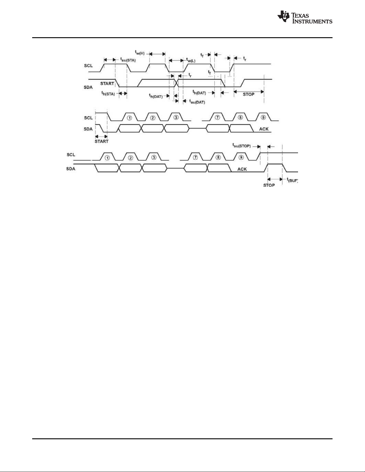
6.6 Timing Requirements
4.5 V ≤ V
ACOK COMPARATOR
t
ACOK_RISE_DEG
t
ACOK_FALL_DEG
INPUT OVERCURRENT COMPARATOR (ACOC)
t
ACOC_DEG
SMBus TIMING CHARACTERISTICS
t
R
t
F
t
W(H)
t
W(L)
t
SU(STA)
t
H(STA)
t
SU(DAT)
t
H(DAT)
t
SU(STOP)
t
(BUF)
F
S(CL)
HOST COMMUNICATION FAILURE
t
timeout
t
BOOT
t
WDI
WDI
t
WDI
PWM DRIVER TIMING
t
DEADTIME_RISE
t
DEADTIME_FALL
(1) Devices participating in a transfer timeout when any clock low exceeds the 25-ms minimum timeout period. Devices that have detected
a timeout condition must reset the communication no later than the 35-ms maximum timeout period. Both a master and a slave must
adhere to the maximum value specified because it incorporates the cumulative stretch limit for both a master (10 ms) and a slave (25
ms).
(2) User can adjust threshold through SMBus ChargeOption() REG0x12.
≤ 24 V, –40°C ≤ TJ≤ 125°C, typical values are at TA= 25°C, with respect to GND (unless otherwise noted)
VCC
PARAMETER MIN TYP MAX UNIT
ACOK rising deglitch to turn on
ACFET; V
ACOK falling deglitch to turn off
ACFET
ACDET
[GBD]
> 2.4V
[GBD]
> V
VCC
1st time or REG0x12[12] = 0
V
> V
VCC
Not 1st time or REG0x12[12] = 1
V
> V
VCC
, ACDET ramps up,
VCC_UVLO
, ACDET ramps up,
VCC_UVLO
, ACDET ramps down 3 µs
VCC_UVLO
100 150 200 ms
0.9 1.3 1.7 s
V
Deglitch time to latch off ACFET 9 12 15 ms
SCLK/SDATA rise time 1 µs
SCLK/SDATA fall time 300 ns
SCLK pulse width high 4 50 µs
SCLK pulse width low 4.7 µs
Setup time for start condition 4.7 µs
Start condition hold time after which first clock pulse is generated 4 µs
Data setup time 250 ns
Data hold time 300 ns
Setup time for stop condition 4 µs
Bus free time between start and stop condition 4.7 µs
Clock frequency 10 100 kHz
SMBus bus release timeout
(1)
25 35 ms
Deglitch for watchdog reset signal 10 ms
Watchdog timeout period, REG0x12 [14:13] = 01
Watchdog timeout period, REG0x12 [14:13] = 10
Watchdog timeout period, REG0x12 [14:13] = 11
(2)
(2)
(2)
(default) 140 175 210
4 5 6
70 88 105
Driver dead time from low side to high side 20 ns
Driver dead time from high side to low side 20 ns
st
Submit Documentation FeedbackCopyright © 2015–2017, Texas Instruments Incorporated
11
Page 12
bq24780S
SLUSC27C –APRIL 2015–REVISED MARCH 2017
Figure 1. SMBus Communication Timing Waveforms
www.ti.com
12
Submit Documentation Feedback Copyright © 2015–2017, Texas Instruments Incorporated
Page 13
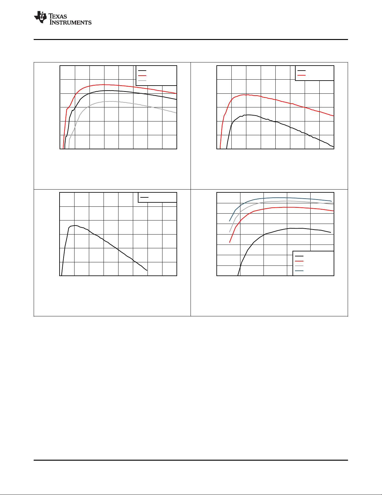
Charge Current (A)
Efficiency
0 1 2 3 4 5 6 7 8
88%
90%
92%
94%
96%
98%
100%
D003
V
BAT
= 3.7 V
Discharge Current (A)
Efficiency
0 2 4 6 8 10
60%
65%
70%
75%
80%
85%
90%
95%
100%
D004
V
BAT
= 3.7 V
V
BAT
= 7.4 V
V
BAT
= 11.1 V
V
BAT
= 14.8 V
Charge Current (A)
Efficiency
0 1 2 3 4 5 6 7 8
88%
90%
92%
94%
96%
98%
100%
D001
V
BAT
= 14.8 V
V
BAT
= 11.1 V
V
BAT
= 7.4 V
Charge Current (A)
Efficiency
0 1 2 3 4 5 6 7 8
88%
90%
92%
94%
96%
98%
100%
D002
V
BAT
= 3.7 V
V
BAT
= 7.4 V
www.ti.com
6.7 Typical Characteristics
bq24780S
SLUSC27C –APRIL 2015–REVISED MARCH 2017
VIN = 20 V
Figure 2. Efficiency During Charging
VIN = 5 V
Figure 4. Efficiency During Charging
VIN = 12 V
Figure 3. Efficiency During Charging
VIN = 20 V
Figure 5. Efficiency During Boost
Submit Documentation FeedbackCopyright © 2015–2017, Texas Instruments Incorporated
13
Page 14

bq24780S
SLUSC27C –APRIL 2015–REVISED MARCH 2017
www.ti.com
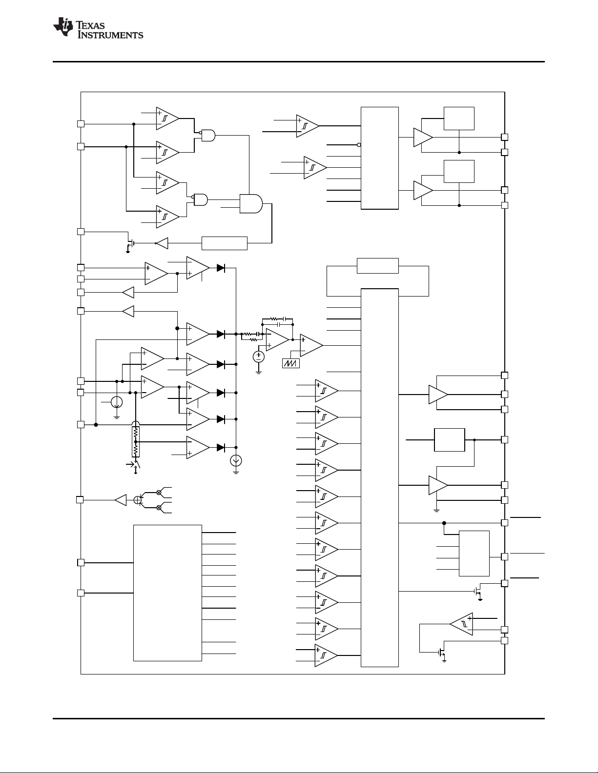
7 Detailed Description
7.1 Overview
The bq24780S is a 1-4 cell battery charge controller with power selection for space-constrained, multi-chemistry
portable applications such as notebook and detachable ultrabook. It supports wide input range of input sources
from 4.5 V to 24 V, and 1-4 cell battery for a versatile solution.
The bq24780S supports automatic system power source selection with separate drivers for n-channel MOSFETS
on the adapter side and battery side.
The bq24780S features Dynamic Power Management (DPM) to limit the input power and avoid AC adapter overloading. During battery charging, as the system power increases, the charging current will reduce to maintain
total input current below adapter rating. If system power demand is temporarily exceeds adapter rating, the
bq24780S supports hybrid power boost mode (previously called "turbo boost mode") to allow battery discharge
energy to supplement system power. For details of hybrid power boost mode, refer to Device Functional Modes
section.
The bq24780S closely monitors system power (PMON), input current (IADP) and battery discharge current
(IDCHG) with highly accurate current sense amplifiers. If current is too high, adapter or battery is removed, a
PROCHOT signal is asserted to CPU so that the CPU optimizes its performance to the power available to the
system.
The SMBus controls input current, charge current and charge voltage registers with high resolution, high
accuracy regulation limits. It also sets the PROCHOT timing and threshold profile to meet system requirements.
14
Submit Documentation Feedback Copyright © 2015–2017, Texas Instruments Incorporated
Page 15
150ms/1.3sec
Rising Deglitch**
20X**
16X
SELECTOR
LOGIC
ACDRV
CHARGE
PUMP
REGN
LDO
SMBUS Interface
ChargeOption()
ChargeCurrent()
ChargeVoltage()
InputCurrent()
DischargeCurrent()
ManufactureID()
DeviceID()
UVLO*
3.2V
WAKEUP*
EN_REGN
ACOVP
0.6V
26V
2.4V
ACGOOD
VCC_SRN
ACOK_DRV
VREF_IAC
VREF_ICHG
ILIM
EN_CHRG
BATOVP
6mA
DAC_VALID
CHARGE_INHIBIT
EN_LEARN
VREF_VREG
VREF_ICHG
VREF_IAC
VREF_IDCHG
EN_BOOST
EN_DPM
10uA
200mV
RAMP
Frequency**
FBO
EAI EAO
PWM
ACOK_DRV
ACDRV
CMSRC+5.9V
ACDRV_CMSRC
ACOC
ACGOOD
CHARGE_INHIBIT
DAC_VALID
EN_LEARN
WATCHDOG
TIMER 175s**
WD_TIMEOUT
EN_CHRG
TYPE III
COMPENSATION
Tj
155C
TSHUT
CHG_OCP
SRP-SRN
120mV
CHG_UCP
5mV
SRP-SRN
LIGHT_LOAD
1.25mV
SRP-SRN
ACOC
ACP_ACN
2x ICRIT*
REFRESH
4.3V
BTST_PH
BATOVP
SRN
104%VREF_VREG
BATLOWV
2.5V
SRN
VCC_SRN
VCC
SRN+275mV
WAKEUP
FAST_DPM
ACP-ACN
107%xVREF_IAC
FET_LATCHOFF_EN
EN_LEARN
EN_REGN
EN_SHIP
FET_LATCHOFF_EN
VCC
ACDET
ACOK
ACP
ACN
IADP
SRP
SRN
SDA
SCL
GND
LODRV
REGN
PHASE
HIDRV
BTST
BATDRV
CMSRC
ACDRV
VREF_VREG
bq24780S
*Threshold is adjustable by registers
28
6
5
2
1
7
20
19
9
22
23
24
27
26
25
18
3
4
PWM
DRIVER
LOGIC
EN_DPM
IDCHG
PMON
BATPRES
15
PROC
HOT
detect
PROCHOT
10
IADPT
IDCHG
VSYS
8
11
12
CMPIN
13
CMPOUT
14
IREF_CMP**
VCC
(ACP-ACN)
BAT
(SRN-SRP)
EN_BOOST
17
BATSRC
BATDRV
CHARGE
PUMP
16
TB_STAT
5X
VREF_IDCHG
ACN
SRN+200mV
ILIM
21
CHG/
DCHG_EN
ILIM
120mV
1X
16X/5
www.ti.com
7.2 Functional Block Diagram
bq24780S
SLUSC27C –APRIL 2015–REVISED MARCH 2017
Submit Documentation FeedbackCopyright © 2015–2017, Texas Instruments Incorporated
15
Page 16

bq24780S
SLUSC27C –APRIL 2015–REVISED MARCH 2017
www.ti.com
7.3 Feature Description
7.3.1 Device Power Up
The bq24780S gets power from adapter or battery. After VCC is above its UVLO threshold, the device wakes up
and starts communication.
7.3.1.1 Battery Only
When VCC voltage is above UVLO, bq24780S powers up to turn on BATFET and starts SMBus communication.
By default, bq24780S stays in low power mode (REG0x12[15] = 1) with lowest quiescent current. When
REG0x12[15] is set to 0, the device enters performance mode. User can enable IDCHG buffer, PMON,
PROCHOT or comparator through SMBus. REGN LDO is enabled (except for IDCHG buffer) for accurate
reference.
7.3.1.2 Adapter Detect and ACOK Output
An external resistor divider attenuates the adapter voltage before it goes to ACDET. The adapter detect
threshold should typically be programmed to a value greater than the maximum battery voltage, but lower than
the maximum allowed adapter voltage. When ACDET is above 0.6V, all bias circuits are enabled.
The open drain ACOK output can be pulled to external rail under the following conditions:
• V
VCC_UVLOZ
• V
ACDET
• V
VCC
The REG0x37[11] tracks the status of ACOK pin. ACOK deglitch time is 150ms at the first time adapter plug-in,
and 1.3 sec at the following plug-ins after VCC or SRN is above its UVLOZ.
> 2.4 V
– V
SRN
< V
VCC
> V
VCC_SRN_FALL
< ACOVP
+ V
VCC_SRN_HYST
7.3.1.2.1 Adapter Overvoltage (ACOVP)
When the VCC pin voltage is higher than 26 V, it is considered adapter over voltage. ACOK is pulled low, and
charge is disabled. ACFET/RBFET are turned off to disconnect the high voltage adapter to system during
ACOVP. BATFET is turned on if turn-on conditions are valid.
When VCC voltage falls below 24 V, it is considered as adapter voltage returns back to normal voltage. ACOK is
pulled high by an external pullup resistor. BATFET is turned off and ACFET and RBFET is turned on to power
the system from the adapter.
7.3.2 System Power Selection
The bq24780S device automatically switches adapter or battery power to system. An automatic break-beforemake logic prevents shoot-through currents when the selectors switch.
The ACDRV drives a pair of common-source (CMSRC) N-channel power MOSFETs (ACFET and RBFET)
between adapter and ACP. The ACFET separates adapter from system and battery, and provides a limited di/dt
when plugging in adapter by controlling the ACFET turn-on time. Meanwhile, it protects the adapter when the
system or battery is shorted. The RBFET provides negative input voltage protection and battery discharge
protection when adapter is shorted to ground, and minimizes system power dissipation with its low R
DS(on)
compared to a Schottky diode.
When the adapter is not present, ACDRV is pulled to CMSRC to keep ACFET and RBFET off, disconnecting the
adapter from the system. BATDRV stays at V
BATSRC
+ 6 V to connect battery to system if all of the following
conditions are valid:
• VCC> V
• V
ACN
< V
UVLO
SRN
+ 200 mV
• ACFET/RBFET off
After the adapter plugs in, the system power source switches from battery to adapter if all of the following
conditions are valid:
• ACOK high
• Not in LEARN mode
• In LEARN mode and V
< battery depletion threshold
SRN
16
Submit Documentation Feedback Copyright © 2015–2017, Texas Instruments Incorporated
Page 17

www.ti.com
Feature Description (continued)
bq24780S
SLUSC27C –APRIL 2015–REVISED MARCH 2017
The gate drive voltage on ACFET and RBFET is V
+ 6 V. If the ACFET/RBFET have been turned on for 20
CMSRC
ms, and the voltage across gate and source is still less than 5.7 V, ACFET and RBFET are turned off. After 1.3s
delay, it resumes turning on ACFET and RBFET. If such a failure is detected seven times within 90 seconds,
ACFET/RBFET are latched off and an adapter removal and system shut down is required to force ACDET < 0.6
V to reset the IC. After IC reset from latch off, ACFET/RBFET can be turned on again. After 90 seconds, the
failure counter is reset to zero to prevent latch off.
To turn off ACFET/RBFET, one of the following conditions must be valid:
• In LEARN mode and V
is above battery depletion threshold;
SRN
• ACOK low
To limit the adapter inrush current during ACFET turn-on, the Cgs and Cgd external capacitor of ACFET must be
carefully selected following the guidelines below:
• Minimize total capacitance on system
• Cgs should be 40× or higher than Cgd to avoid ACFET false turn on during adapter hot plug-in
• Fully turn on ACFET within 20 ms, otherwise, charger IC will consider turn-on failure
• Check with MOSFET vendor on peak current rating
• Place 4-kΩ resistor in series with ACDRV, CMSRC, and BATDRV pin to limit inrush current.
7.3.3 Enable and Disable Charging
In charge mode, the following conditions have to be valid to start charge:
• Charge is enabled through SMBus (REG0x12[0], default is 0, charge enabled)
• ILIM pin voltage is higher than 120 mV
• All ChargeCurrent(), ChargeVoltage() and InputCurrent() registers have valid value programmed
• ACOK is valid (see Device Power Up for details)
• ACFET and RBFET turn on and gate voltage is high enough (see System Power Selection for details)
• V
does not exceed BATOVP threshold
SRN
• IC temperature does not exceed TSHUT threshold
• Not in ACOC condition (see Device Protections Features for details)
One of the following conditions stops on-going charging:
• Charge is inhibited through SMBus(REG0x12[0]=1)
• ILIM pin voltage is lower than 60 mV
• One of three registers is set to 0 or out of range
• ACOK is pulled low (see Device Power Up for details)
• ACFET turns off
• V
exceeds BATOVP threshold
SRN
• TSHUT IC temperature threshold is reached
• ACOC is detected (see Device Protections Features for details)
• Short circuit is detected (see Inductor Short, MOSFET Short Protection for details)
• Watchdog timer expires if watchdog timer is enabled (see Charger Timeout for details)
7.3.3.1 Automatic Internal Soft-Start Charger Current
Every time the charge is enabled, the charger automatically applies soft-start on charge current to avoid any
overshoot or stress on the output capacitors or the power converter. The charge current starts at 128 mA, and
the step size is 64 mA in CCM mode for a 10 mΩ current sensing resistor. Each step lasts around 400 μs in
CCM mode, till it reaches the programmed charge current limit. No external components are needed for this
function.
During DCM mode, the soft start up current step size is larger and each step lasts for longer time period due to
the intrinsic slow response of DCM mode.
Submit Documentation FeedbackCopyright © 2015–2017, Texas Instruments Incorporated
17
Page 18

bq24780S
SLUSC27C –APRIL 2015–REVISED MARCH 2017
www.ti.com
Feature Description (continued)
7.3.4 Current and Power Monitor
7.3.4.1 High Accuracy Current Sense Amplifier (IADP and IDCHG)
As an industry standard, a high-accuracy current sense amplifier (CSA) is used to monitor the input current
(IADP) and the discharge current (IDCHG). IADP voltage is 20X or 40X the differential voltage across ACP and
ACN. IDCHG voltage is 8X or 16X the differential voltage across SRN and SRP. After VCC is above UVLO and
ACDET is above 0.6 V, IADP output becomes valid. .
A maximum 100-pF capacitor is recommended to connect on the output for decoupling high-frequency noise. An
additional RC filter is optional, if additional filtering is desired. Note that adding filtering also adds additional
response delay. The CSA output voltage is clamped at 3.3 V. To lower the voltage on current monitoring, a
resistor divider from CSA output to GND can be used and accuracy over temperature can still be achieved
7.3.4.2 High Accuracy Power Sense Amplifier (PMON)
The bq24780S device monitors total available power from adapter and battery together. The ratio of PMON
voltage and total power K
allows input sense resistor 2x or 1/2x of charge sense resistor by setting REG0x3B[13:12] to 1.
I
PMON
= K
PMON(VIN
x IIN- V
A resistor is connected on the PMON pin to converter output current to output voltage. A maximum 100-pF
capacitor is recommended to connect on the output for decoupling high-frequency noise. An additional RC filter
is optional, if additional filtering is desired. Note that adding filtering also adds additional response delay. The
PMON output voltage is clamped to 3.3 V.
can be programmed in REG0x3B[9] with default 1 µA/W. The bq24780S device
PMON
x I
) (I
BAT
BAT
> 0 during charge; I
BAT
< 0 during discharge) (1)
BAT
7.3.5 Processor Hot Indication for CPU Throttling
When CPU is running turbo mode, the peak power may exceed total available power from adapter and battery.
The adapter current and battery discharge overshoot, or system voltage drop indicates the system power may be
too high. When the adapter or battery is removed, the remaining power source may not support the peak power
in turbo mode. The processor hot function in bq24780S monitors these events, and PROCHOT pulse is asserted.
The PROCHOT triggering events include:
• ICRIT: adapter peak current
• INOM: adapter average current (110% of input current limit)
• IDCHG: battery discharge current
• VSYS: system voltage on SRN for 2s - 4s battery
• ACOK: upon adapter removal (ACOK pin HIGH to LOW)
• BATPRES: upon battery removal (BATPRES pin LOW to HIGH)
• CMPOUT: Independent comparator output (CMPOUT pin HIGH to LOW)
The threshold of ICRIT, IDCHG or VSYS, and the deglitch time of ICRIT, INOM, IDCHG or CMPOUT are
programmable through SMBus. Each triggering event can be individually enabled in REG0x3D[6:0].
18
Submit Documentation Feedback Copyright © 2015–2017, Texas Instruments Incorporated
Page 19

o
o o
1
f
2 L C
S
IADP
INOM
IDCHG
Ref_DCHG
Ref
10-ms
Debounce
VSRP
1.05 V
50W
PROCHOT
≥10 ms
Adjustable
Deglitch
ICRIT
< 0.3 V
BATPRES
(One shot on rising edge)
20- sm
Deglitch
ACOK
(One shot on falling edge)
CMPOUT
www.ti.com
Feature Description (continued)
bq24780S
SLUSC27C –APRIL 2015–REVISED MARCH 2017
Figure 6. PROCHOT Profile
When any event in PROCHOT profile is triggered, PROCHOT is asserted low for minimum 10 ms (default
REG0x3C[4:3]=10). At the end of the 10 ms, if the PROCHOT event is still active, the pulse gets extended.
During one cycle of PROCHOT, all the triggering events are saved in status register REG0x3A[6:0] for easy test
debug and system optimization.
7.3.6 Converter Operation
The synchronous buck PWM converter uses a fixed frequency voltage control scheme and internal type III
compensation network. The LC output filter gives a characteristic resonant frequency:
The resonant frequency, fo, is used to determine the compensation to ensure there is sufficient phase margin for
the target bandwidth. The LC output filter should be selected to give a resonant frequency of 10- to 20-kHz
nominal for the best performance. Suggested component value for a charge current of 800-kHz default switching
frequency is shown in Table 1:
Table 1. Suggest Component Value for Charge Current of 800-kHz Default Switching Frequency
CHARGE CURRENT 2A 3A 4A 6A 8A
Output Inductor Lo (µH) 6.8 or 8.2 5.6 or 6.8 3.3 or 4.7 3.3 2.2
Output Capacitor Co (µF) 20 20 20 30 40
Sense Resistor (mΩ) 10 10 10 10 10
Ceramic capacitors show a DC-bias effect. This effect reduces the effective capacitance when a DC-bias voltage
is applied across a ceramic capacitor, as on the output capacitor of a charger. The effect may lead to a
significant capacitance drop, especially for high output voltages and small capacitor packages. See the
manufacturer's data sheet about the performance with a DC bias voltage applied. It may be necessary to choose
a higher voltage rating or nominal capacitance value to get the required value at the operating point.
(2)
Submit Documentation FeedbackCopyright © 2015–2017, Texas Instruments Incorporated
19
Page 20

bq24780S
SLUSC27C –APRIL 2015–REVISED MARCH 2017
www.ti.com
7.3.6.1 Continuous Conduction Mode (CCM)
With sufficient charge current, the inductor current does not cross 0, which is defined as CCM. The controller
starts a new cycle with ramp coming up from 200 mV. As long as EAO voltage is above the ramp voltage, the
high-side MOSFET (HSFET) stays on. When the ramp voltage exceeds EAO voltage, HSFET turns off and lowside MOSFET (LSFET) turns on. At the end of the cycle, ramp gets reset and LSFET turns off, ready for the next
cycle. There is always break-before-make logic during transition to prevent cross-conduction and shoot-through.
During the dead time when both MOSFETs are off, the body-diode of the low-side power MOSFET conducts the
inductor current.
During CCM, the inductor current always flows and creates a fixed two-pole system. Having the LSFET turn-on
keeps the power dissipation low and allows safe charging at high currents.
7.3.6.2 Discontinuous Conduction Mode (DCM)
During the HSFET off time when LSFET is on, the inductor current decreases. If the current goes to 0, the
converter enters DCM. Every cycle, when the voltage across SRP and SRN falls below 5 mV (0.5 A on 10 mΩ),
the undercurrent-protection comparator (UCP) turns off LSFET to avoid negative inductor current, which may
boost the system through the body diode of HSFET.
During DCM the loop response automatically changes. It changes to a single-pole system and the pole is
proportional to the load current.
7.3.6.3 Non-Sync Mode and Light Load Comparator
As the charge current is below 125 mA (on 10-mΩ sense resistor), the light load comparator keeps LSFET off.
The converter enters non-sync mode. With LSFET, body diode blocks negative current in the inductor so that no
current flows back to the input. As charge current rises above 250 mA, LSFET turns on again.
7.3.6.4 EMI Switching Frequency Adjust
The charger switching frequency can be adjusted 600 kHz or 1 MHz to solve EMI issues through SMBus
command REG0x12[9:8].
7.3.7 Battery LEARN Cycle
A battery LEARN cycle can be activated through the REG0x12[5]. When LEARN is enabled, the system receives
power from the battery instead of the adapter turning off ACFET/RBFET and turning on BATFET. The LEARN
function allows the battery to discharge in order to calibrate the battery gas gauge over a complete discharge
and charge cycle. The controller automatically exits the LEARN cycle when the battery voltage is below the
battery depletion threshold. The system switches back to adapter input by turning off BATFET and turning on
ACFET/RBFET. After the LEARN cycle, REG0x12[5] is automatically reset to 0.
When the battery is removed during LEARN mode, BATPRES rises from low to high and the device exits LEARN
mode. ACFET/RBFET quickly turns on in 100µs to prevent the system from crashing. The turn-on triggered by
BATPRES is faster than that triggered by battery depletion comparator.
7.3.8 Charger Timeout
The bq24780S device includes a watchdog timer to terminate charging or hybrid power boost mode if the charger
does not receive a write ChargeVoltage() or write ChargeCurrent() command within 175 s (adjustable through
0x12[14:13] command).
If a watchdog timeout occurs, all register values keep unchanged, but converter is suspended. A write to
ChargeVoltage(), or ChargeCurrent(), or change REG0x12[14:13] resets watchdog timer and resumes converter
for charging or hybrid power boost mode. The watchdog timer can be disabled, or set to 5, 88, or 175 s through
SMBus command REG0x12[14:13]).
20
Submit Documentation Feedback Copyright © 2015–2017, Texas Instruments Incorporated
Page 21

bq24780S
www.ti.com
SLUSC27C –APRIL 2015–REVISED MARCH 2017
7.3.9 Device Protections Features
7.3.9.1 Input Overcurrent Protection (ACOC)
The bq24780S device cannot maintain the input current level if the charge current has been already reduced to
0. When the input current exceeds 1.25x or 2x of ICRIT set point (with 12-ms blank-out time), ACFET/RBFET is
latches off and an adapter removal is required to force ACDET < 0.6 V to reset IC. After IC reset from latch off,
ACFET/RBFET can be turned on again.
The ACOC function threshold can be set to 1.25x or 2x of ICRIT (REG37[9]) current or disabled through SMBus
command (REG0x37[10]).
7.3.9.2 Charge Overcurrent Protection (CHGOCP)
The bq24780S device has cycle-by-cycle peak overcurrent protection. It monitors the voltage across SRP and
SRN, and prevents the current from exceeding the threshold based on the charge current set point. The highside gate drive turns off for the rest of the cycle when over current is detected, and resumes when the next cycle
starts.
The charge OCP threshold is automatically set to 6, 9, and 12 A on a 10-mΩ current sensing resistor based on
charge current register value. This prevents the threshold from being too high, which is not safe, or too low,
which can be triggered in typical operation. Select proper inductance to prevent OCP triggering in typical
operation due to high inductor current ripple.
7.3.9.3 Battery Overvoltage Protection (BATOVP)
The bq24780S device does not allow the high-side and low-side MOSFET to turn-on when the battery voltage at
SRN exceeds 104% of the regulation voltage set point. If BATOVP lasts over 30 ms, charger is completely
disabled. This allows a quick response to an overvoltage condition – such as when the load is removed or the
battery is disconnected. A 6-mA current sink from SRP to GND is only on during BATOVP and allows
discharging the stored output inductor energy that is transferred to the output capacitors.
7.3.9.4 Battery Short
When battery voltage on SRN falls below 2.5 V, the converter resets for 1 ms and resumes charge if all the
enable conditions in the Enable and Disable Charging section are satisfied. This prevents overshoot current in
the inductor, which can saturate the inductor and may damage the MOSFET. The charge current is limited to 0.5
A on 10-mΩ current sensing resistor when BATLOWV condition persists and LSFET keeps off. The LSFET turns
on only for a refreshing pulse to charge BTST capacitor.
7.3.9.5 Thermal Shutdown Protection (TSHUT)
The WQFN package has low thermal impedance, which provides good thermal conduction from the silicon to the
ambient, to keep junction temperatures low. As an added level of protection, the charger converter turns off for
self-protection whenever the junction temperature exceeds the 155°C. The charger stays off until the junction
temperature falls below 135°C. During thermal shutdown, the REGN LDO current limit is reduced to 14 mA.
Once the temperature falls below 135°C, charge can be resumed with soft start.
7.3.9.6 Inductor Short, MOSFET Short Protection
The bq24780S device has a unique short circuit protection feature. Its cycle-by-cycle current monitoring feature
is achieved through monitoring the voltage drop across RDS(on) of the MOSFETs after a certain amount of
blanking time. In case of a MOSFET short or inductor short circuit, the overcurrent condition is sensed by two
comparators and two counters are triggered. After seven short circuit events, the charger is latched off and
ACFET and RBFET are turned off to disconnect the adapter from the system. BATFET is turned on to connect
the battery pack to the system. To reset the charger from latch-off status, the IC VCC pin must be pulled below
UVLO or the ACDET pin must be pulled below 0.6 V. This can be achieved by removing the adapter and shutting
down the operation system. The low-side MOSFET Vds monitor circuit is enabled by REG0x37[7], and the
threshold is 750 mV. The high-side MOSFET Vds monitor circuit is enabled by REG0x37[6], and the threshold is
250 mV. During boost function, the low-side MOSFET short circuit protection threshold is used for cycle-by-cycle
current limiting, charger does not latch up.
Submit Documentation FeedbackCopyright © 2015–2017, Texas Instruments Incorporated
21
Page 22

bq24780S
SLUSC27C –APRIL 2015–REVISED MARCH 2017
www.ti.com
Due to the amount of blanking time to prevent noise when MOSFET just turns on, the cycle-by-cycle charge
overcurrent protection may detect high current and turn off MOSFET first before the short circuit protection circuit
can detect short condition because the blanking time has not finished. In such a case, the charger may not be
able to detect a short circuit and the counter may not be able to count to seven then latch off. Instead the
charger may continuously keep switching with very narrow duty cycle to limit the cycle-by-cycle current peak
value. However, the charger should still be safe and does not cause failure because the duty cycle is limited to a
very short time and the MOSFET should still be inside the safety operation area. During a soft start period, it may
take a long time instead of just seven switching cycles to detect short circuit based on the same blanking time
reason.
7.4 Device Functional Modes
7.4.1 Battery Charging
The bq24780S charges 1-4 cell battery in constant current (CC), and constant voltage (CV) mode. The host
programs battery voltage in REG0x15(). According to battery voltage, the host programs appropriate charge
current in REG0x14(). When battery is full or battery is not in good condition to charge, host terminates charge
by setting REG0x12[0] to 1, or setting either ChargeVoltage() or ChargeCurrent() to zero.
See the Feature Description section for details on charge enable conditions and register programming.
7.4.2 Hybrid Power Boost Mode
The bq24780S device supports the hybrid power boost mode by allowing battery discharge energy to system
when system power demand is temporarily higher than adapter maximum power level so the adapter does not
crash. After device powers up, the REG0x37[2] is 0 to disable hybrid power boost mode. To enable hybrid power
boost mode, host writes 1 to REG0x37[2]. The TB_STAT pin and REG0x37[1] indicate if the device is in hybrid
power boost mode.
To support hybrid power boost mode, input current must be set higher than 1536 mA for 10 mΩ input current
sensing resistor. When input current is higher than 107% of input current limit in REG0x3F(), charger IC allows
battery discharge and charger converter changes from buck converter to boost converter. During hybrid power
boost mode the adapter current is regulated at input current limit level so that adapter will not crash. The battery
discharge current depends on system current requirement and adapter current limit. The watchdog timer can be
enabled to prevent converter running at hybrid power boost mode for too long.
7.4.2.1 Battery Discharge Current Regulation in Hybrid Power Boost Mode
To keep the discharge current below battery OCP rating during boost mode, the bq24780S device supports
discharge current regulation. After device powers up, the REG0x37[15] is 0 to disable discharge current
regulation. To enable discharge current regulation, host writes 1 to REG0x37[15].
Once the battery discharge current is limited, the input current goes up to meet the system current requirement.
The user can assert PROCHOT to detect input current increase (ICRIT or INOM), and request CPU throttling to
lower the system power.
22
Submit Documentation Feedback Copyright © 2015–2017, Texas Instruments Incorporated
Page 23

bq24780S
www.ti.com
SLUSC27C –APRIL 2015–REVISED MARCH 2017
7.5 Programming
7.5.1 SMBus Interface
The bq24780S device operates as a slave, receiving control inputs from the embedded controller host through
the SMBus interface. The bq24780S device uses a simplified subset of the commands documented in System
Management Bus Specification V1.1, which can be downloaded from www.smbus.org. The bq24780S device
uses the SMBus read-word and write-word protocols (shown in Table 2 and Table 3) to communicate with the
smart battery. The bq24780S device performs only as a SMBus slave device with address 0b00010010 (0x12H)
and does not initiate communication on the bus. In addition, the device has two identification registers, a 16-bit
device ID register (0xFFH) and a 16-bit manufacturer ID register (0xFEH).
SMBus communication starts when VCC is above UVLO.
The data (SDA) and clock (SCL) pins have Schmitt-trigger inputs that can accommodate slow edges. Choose
pullup resistors (10 kΩ) for SDA and SCL to achieve rise times according to the SMBus specifications.
Communication starts when the master signals a start condition, which is a high-to-low transition on SDA, while
SCL is high. When the master has finished communicating, the master issues a stop condition, which is a low-tohigh transition on SDA, while SCL is high. The bus is then free for another transmission. Figure 7 and Figure 8
show the timing diagram for signals on the SMBus interface. The address byte, command byte, and data bytes
are transmitted between the start and stop conditions. The SDA state changes only while SCL is low, except for
the start and stop conditions. Data is transmitted in 8-bit bytes and is sampled on the rising edge of SCL. Nine
clock cycles are required to transfer each byte in or out of the bq24780S device because either the master or the
slave acknowledges the receipt of the correct byte during the ninth clock cycle. The bq24780S supports the
charger commands listed in Table 2.
7.5.1.1 SMBus Write-Word and Read-Word Protocols
Table 2. Write-Word Format
S
(1)(2)
(1) Master to slave
(2) S = Start condition or repeated start condition
(3) W = Write bit (logic-low)
(4) Slave to master (shaded gray)
(5) ACK = Acknowledge (logic-low)
(6) P = Stop condition
SLAVE
ADDRESS
(1)W(1)(3)
ACK
(4)(5)
COMMAND
(1)
BYTE
ACK
(4)(5)
LOW DATA
(1)
BYTE
ACK
(4)(5)
HIGH DATA
BYTE
7 bits 1b 1b 8 bits 1b 8 bits 1b 8 bits 1b
MSB LSB 0 0 MSB LSB 0 MSB LSB 0 MSB LSB 0
Table 3. Read-Word Format
(1)
S
(2)
SLAVE
ADDRESS
(1)W(1)(3)
ACK
(4)(5)
COMMAND
(1)
BYTE
7 bits 1b 1b 8 bits 1b 7 bits 1b 1b 8 bits 1b 8 bits 1b
MSB LSB 0 0 MSB LSB 0 MSB LSB 1 0 MSB LSB 0 MSB LSB 1
(1) Master to slave
(2) S = Start condition or repeated start condition
(3) W = Write bit (logic-low)
(4) Slave to master (shaded gray)
(5) ACK = Acknowledge (logic-low)
(6) R = Read bit (logic-high)
(7) NACK = Not acknowledge (logic-high)
(8) P = Stop condition
ACK
(4)(5)
(1)
S
(2)
SLAVE
ADDRESS
(1)
R
ACK
(1)
(6)
(4)(5)
LOW DATA
BYTE
ACK
(1)(5)
HIGH DATA
(4)
(1)
BYTE
(4)
ACK
(4)(5)
NACK
P
(1)(6)
(1)(7)P(1)(8)
Submit Documentation FeedbackCopyright © 2015–2017, Texas Instruments Incorporated
23
Page 24

A B C D E F G H I J K
t
LOW
t
HIGH
SMBCLK
SMBDATA
t
SU:STA
t t
HD:STA SU:DAT
HD:DAT SU:DAT
t t
t
SU:STOtBUF
A = START CONDITION E = SLAVE PULLS SMBDATA LINE LOW I = ACKNOWLEDGE CLOCK PULSE
A B C D E F G H I J K L M
t
LOW
t
HIGH
SMBCLK
SMBDATA
t
SU:STAtHD:STA
SU:DAT
t
t
HD:DAT
HD:DAT
t
t
SU:STOtBUF
bq24780S
SLUSC27C –APRIL 2015–REVISED MARCH 2017
7.5.1.2 Timing Diagrams
A = Start condition H = LSB of data clocked into slave
B = MSB of address clocked into slave I = Slave pulls SMBDATA line low
C = LSB of address clocked into slave J = Acknowledge clocked into master
D = R/W bit clocked into slave K = Acknowledge clock pulse
E = Slave pulls SMBDATA line low L = Stop condition, data executed by slave
F = ACKNOWLEDGE bit clocked into master M = New start condition
G = MSB of data clocked into slave
www.ti.com
Figure 7. SMBus Write Timing
A = Start condition G = MSB of data clocked into master
B = MSB of address clocked into slave H = LSB of data clocked into master
C = LSB of address clocked into slave I = Acknowledge clock pulse
D = R/W bit clocked into slave J = Stop condition
E = Slave pulls SMBDATA line low K = New start condition
F = ACKNOWLEDGE bit clocked into master
24
Submit Documentation Feedback Copyright © 2015–2017, Texas Instruments Incorporated
Figure 8. SMBus Read Timing
Page 25

bq24780S
www.ti.com
SLUSC27C –APRIL 2015–REVISED MARCH 2017
7.6 Register Maps
7.6.1 Battery-Charger Commands
The bq24780S supports thirteen battery-charger commands that use either Write-Word or Read-Word protocols,
as summarized in Table 4. ManufacturerID() and DeviceID() can be used to identify the bq24780S. The
ManufacturerID() command always returns 0x0040H and the DeviceID() command always returns 0x0030H.
Table 4. Battery Charger Command Summary
REGISTER ADDRESS REGISTER NAME READ OR WRITE DESCRIPTION POR STATE
0x12H ChargeOption0() Table 5 Read or Write Charge Options Control 0 0xE108H
0x3BH ChargeOption1() Table 6 Read or Write Charge Options Control 1 0xC210H
0x38H ChargeOption2()Table 7 Read or Write Charge Options Control 2 0x0384H
0x37H ChargeOption3()Table 8 Read or Write Charge Options Control 3 0x1A40H
0x3CH ProchotOption0()Table 9 Read or Write PROCHOT Options Control 0 0x4A54H
0x3DH ProchotOption1() Table 10 Read or Write PROCHOT Options Control 1 0x8120H
0x3AH ProchotStatus() Table 11 Read Only PROCHOT status 0x0000H
0x14H ChargeCurrent() Table 12 Read or Write 7-bit Charge Current Setting 0x0000H
0x15H ChargeVoltage() Table 13 Read or Write 11-bit Charge Voltage Setting 0x0000H
0x39H DischargeCurrent() Table 15 Read or Write 6-bit Discharge Current Setting 0x1800H, or 6144mA
0x3FH InputCurrent() Table 14 Read or Write 6-bit Input Current Setting 0x1000H, or 4096mA
0xFEH ManufacturerID() Read Only Manufacturer ID 0x0040H
0xFFH DeviceID() Read Only Device ID 0x30H
Submit Documentation FeedbackCopyright © 2015–2017, Texas Instruments Incorporated
25
Page 26

bq24780S
SLUSC27C –APRIL 2015–REVISED MARCH 2017
7.6.2 Setting Charger Options
7.6.2.1 ChargeOption0 Register
Figure 9. ChargeOption0 Register (0x12H)
15 14 13 12 11 10 9 8
Low Power
WATCHDOG Timer Adjust Reserved Switching Frequency
Mode Enable
R/W R/W R R/W
7 6 5 4 3 2 1 0
Reserved LEARN Mode
Enable
IADP Amplifier
Gain for
IDCHG Amplifier
Ratio
Reserved Charge Inhibit
Primary Input
R R/W R/W R/W R R/W
LEGEND: R/W = Read/Write; R = Read only; -n = value after reset
Table 5. ChargeOption0 Register (0x12H)
BIT BIT NAME DESCRIPTION
0: IC in performance mode with battery only. The PROCHOT, current/power monitor buffer and independent
[15]
[14:13]
[12:10] Reserved 0- Reserved
[9:8]
[7:6] Reserved 0 - Reserved
[5]
[4]
[3]
[2:1] Reserved 0 - Reserved
[0]
Low Power Mode Enable
(EN_LWPWR)
WATCHDOG Timer Adjust
(WDTMR_ADJ)
Switching Frequency
(PWM_FREQ)
LEARN Mode Enable
(EN_LEARN)
IADP Amplifier Gain for Primary
Input
(IADP_GAIN)
IDCHG Amplifier Gain
(IDCHG_GAIN)
Charge Inhibit
(CHRG_INHIBIT)
comparator follow register setting.
1: IC in low power mode with battery only. IC is in the lowest quiescent current when this bit is enabled.
PROCHOT, discharge current monitor buffer, power monitor buffer and independent comparator are disabled
(default at POR)
Set maximum delay between consecutive SMBus write charge voltage or charge current command.
If IC does not receive write on REG0x14() or REG0x15() within the watchdog time period, the charger converter
stops to disable charge and boost mode operation.
After expiration, the timer will resume upon the write of REG0x14() or REG0x15(). The charge or boost
operation will resume if all the other conditions are valid.
00: Disable watchdog timer
01: Enabled, 5 sec
10: Enabled, 88 sec
11: Enable watchdog timer (175 s) (default at POR)
Converter switching frequency.
00: 600 kHz
01: 800 kHz (default at POR)
10: 1 MHz
11: Reserved
Battery LEARN mode enable. In LEARN mode, ACFET and RBFET turns off and BATFET turns on. When
/BATPRES is HIGH, IC exits LEARN mode and this bit is set back to 0. When the battery is depleted, the
charger cannot enable LEARN mode
0: Disable LEARN mode (default at POR)
1: Enable LEARN mode
Ratio of IADP pin voltage over the voltage across ACP and ACN.
0: 20X (default at POR)
1: 40X
Ratio of IDCHG pin voltage over the voltage across SRN and SRP. 0: 8x with discharge current regulation range
0-32A.
0: 8x with discharge current regulation range 0-32A.
1: 16x with discharge current regulation range (default at POR)
Charge inhibit. When this bit is 0, battery charging is enabled with valid value in REG0x14() and REG0x15()
0: Enable charge (default at POR)
1: Inhibit charge
www.ti.com
26
Submit Documentation Feedback Copyright © 2015–2017, Texas Instruments Incorporated
Page 27

www.ti.com
SLUSC27C –APRIL 2015–REVISED MARCH 2017
7.6.3 ChargeOption1 Register Figure 10. ChargeOption1 Register (0x3BH)
15 14 13 12 11 10 9 8
BAT Depletion Comparator
Threshold
Input/Discharge Sense
Resistor Ratio R
EN_IDCHG EN_PMON PMON Gain Reserved
R/W R/W R/W R/W R/W R
7 6 5 4 3 2 1 0
Independent
Comparator
Reference
Independent
Comparator
Polarity
Independent Comparator
Deglitch Time
Power Path Latch-
off Enable
Reserved Discharge
SRN for
Shipping
Mode_EN
R/W R/W R/W R/W R R/W R
LEGEND: R/W = Read/Write; R = Read only; -n = value after reset
Table 6. ChargeOption1 Register (0x3BH)
BIT BIT NAME DESCRIPTION
Battery over-discharge threshold.During LEARN cycle, when battery voltage is below the depletion threshold,
the IC exits LEARN mode. During boost mode, when battery voltage is below the depletion threshold, the IC
[15:14]
[13:12] (RSNS_RATIO)
[11] EN_IDCHG
[10] EN_PMON
[9]
[8] Reserved 0 - Reserved
[7]
[6]
[5:4]
[3]
[2] Reserved 0 - Reserved
[1]
[0] Reserved 0 - Reserved
Battery Depletion Threshold
(BAT_DEPL_VTH)
PMON Gain
(PMON_RATIO)
Independent Comparator
Reference (CMP_REF)
Independent Comparator Polarity
(CMP_POL)
Independent Comparator Deglitch
Time (CMP_DEG)
Power Path Latch-off Enable
(EN_FET_LATCHOFF )
Discharge SRN for Shipping
Mode (EN_SHIP_DCHG)
exits boost mode.
00: Falling threshold = 59.19% of voltage regulation limit (~2.486V/cell)
01: Falling threshold = 62.65% of voltage regulation limit (~2.631V/cell)
10: Falling threshold = 66.55% of voltage regulation limit (~2.795V/cell)
11: Falling threshold = 70.97% of voltage regulation limit (2.981V/cell) (default at POR)
0 - Adjust the PMON calculation with different input sense resistor RAC and charge sense resistor RSR.
00: RACand R
1:1 (default at POR)
01: RACand RSR2:1
10: RACand RSR1:2
11: Reserved
IDCHG pin output enable.
0: Disable IDCHG output to minimize Iq (default at POR)
1: Enable IDCHG output
PMON pin output enable.
0: Disable PMON output to minimize Iq (default at POR)
1: Enable PMON output
Ratio of PMON output current vs total input and battery power with 10 mΩ sense resistor.
0: 0.25 µA/W
1: 1 µA/W (default at POR)
With the sense resistor is 20/10 mΩ, or 10/20 mΩ, or 20/20mΩ (RACand RSR)
0: 0.5 µA/W
1: 2 µA/W (default at POR)
Independent comparator internal reference.
0: 2.3 V (default at POR)
1: 1.2 V
Independent comparator output polarity
0: When CMPIN is above internal threshold, CMPOUT is LOW (default at POR)
1: When CMPIN is above internal threshold, CMPOUT is HIGH
Independent comparator deglitch time, applied on the edge where CMPOUT goes LOW. No deglitch time is
applied on the rising edge of CMPOUT.
00: Independent comparator is disabled
01: Independent comparator is enabled with output deglitch time 1 µs (default at POR)
10: Independent comparator is enabled with output deglitch time 2 ms
11: Independent comparator is enabled with output deglitch time 5 sec
When independent comparator is triggered, both ACFET/RBFET turn off. The latch off is cleared by either POR
or write this bit to zero.
0: When independent comparator is triggered, no power path latch off (default at POR)
1: When independent comparator is triggered, power path latches off.
Discharge SRN pin for 140 ms with minimum 5-mA current. When 140 ms is over, this bit is reset to 0.
0 : Disable discharge mode (default at POR)
1: Enable discharge mode
SR
bq24780S
Reserved
Submit Documentation FeedbackCopyright © 2015–2017, Texas Instruments Incorporated
27
Page 28

bq24780S
SLUSC27C –APRIL 2015–REVISED MARCH 2017
7.6.4 ChargeOption2 Register
Figure 11. ChargeOption2 Register (0x38H)
15 14 13 12 11 10 9 8
Reserved Reserved
R R
7 6 5 4 3 2 1 0
Independent
Reserved Reserved Reserved
External
Current Limit
Enable
R/W R R R
LEGEND: R/W = Read/Write; R = Read only; -n = value after reset
Table 7. ChargeOption2 Register (0x38H)
BIT BIT NAME DESCRIPTION
[15:10] Reserved 0– Reserved
[9:8] Reserved 1 - Reserved
[7]
[6:3] Reserved 0 - Reserved
[2] Reserved 1 - Reserved
[1:0] Reserved 0 - Reserved
External Current Limit Enable
(EN_EXTILIM)
External ILIM pin enable to set the charge and discharge current.
0: Charge/discharge current limit is set by REG0x14() and 0x39().
1: Charge/discharge current limit is set by the lower value of ILIM pin and registers. (default at POR)
www.ti.com
28
Submit Documentation Feedback Copyright © 2015–2017, Texas Instruments Incorporated
Page 29

www.ti.com
SLUSC27C –APRIL 2015–REVISED MARCH 2017
7.6.5 ChargeOption3 Register
Figure 12. ChargeOption3 Register (0x37H)
15 14 13 12 11 10 9 8
Discharge
Current
Regulation
Enable
Reserved ACOK
Deglitch Time
for Primary
Input
Adapter Present
Indicator
ACOC Enable ACOC Limit Reserved
R/W R R/W R/W R/W R/W R
7 6 5 4 3 2 1 0
HSFET VDS
Threshold
LSFET VDS
Threshold
Fast DPM
Threshold
Fast DPM Deglitch Time Hybrid Power
Boost Mode
Boost Mode
Indication
Enable
R/W R/W R/W R/W R/W R/W R
LEGEND: R/W = Read/Write; R = Read only; -n = value after reset
Table 8. ChargeOption3 Register (0x37H)
BIT BIT NAME DESCRIPTION
[15]
[14:13] Reserved 0 - Reserved
[12]
[11]
[10] ACOC Enable (EN_ACOC)
[9] ACOC Limit (ACOC_VTH)
[8] Reserved 0 – Reserved
[7]
[6]
[5]
[4:3]
[2]
[1]
[0] Reserved 0 – Reserved
Discharge Current Regulation
Enable(EN_IDCHG_REG)
ACOK Deglitch Time for Primary
Input (ACOK_DEG )
Adapter Present Indicator
(ACOK_STAT )
HSFET VDS Threshold
(IFAULT_HI)
LSFET VDS Threshold
(IFAULT_LO)
Fast DPM Threshold
(FDPM_VTH)
Fast DPM Deglitch Time
(FDPM_DEG)
Hybrid Power Boost Mode Enable
(EN_BOOST)
Boost Mode Indication
(BOOST_STAT)
Battery discharge current regulation enable.
0: Disable discharge current regulation (default at POR)
1: Enable discharge current regulation
Adjust ACOK rising edge deglitch time.
After POR, the first time adapter plugs in, deglitch time is always 150 ms regardless of register bit. Starting from
the 2nd time adapter plugs in, the deglitch time follows the bit setting. During system over-current, or system
short when ACDET is pulled below 2.4 V, 1.3 sec deglitch time keeps ACFET/RBFET turn off long enough
before the next turn on.
0: ACOK rising edge deglitch time 150ms
1: ACOK rising edge deglitch time 1.3 sec (default at POR)
Input present indicator. Same logic as ACOK pin. This bit is read only.
0: AC adapter is not present
1: AC adapter is present
ACOC protection threshold by monitoring ACP_ACN voltage.
0: Disable ACOC (default at POR)
1: Enable ACOC
ACOC protection threshold by monitoring ACP_ACN voltage.
0: 125% of ICRIT
1: 200% of ICRIT (default at POR)
MOSFET/inductor short protection by monitoring high side MOSFET drain-source voltage.
0: Disable (default at POR)
1: 750 mV
MOSFET/inductor short protection by monitoring low side MOSFET drain-source voltage. Also as cycle-by-cycle
current limit protection threshold during boost function.
0: Disable
1: 250 mV (default at POR)
Fast DPM comparator threshold to enter hybrid power boost mode. (Minimum DPM setting for boost mode:
1536 mA)
0: 107% (falling 93%)(<default at POR)
1: 115% (falling 85%)
Response time from system current exceeding Fast DPM Threshold to battery discharge in boost mode.
00: Response time 150 µs (default at POR)
01: Response time 250 µs
1X: Response time 50 µs
Boost mode enable bit. When /BATPRES goes from LOW to HIGH (battery removal), this bit will be reset to
zero to disable boost mode.
0: Disable hybrid power boost mode (default at POR)
1: Enable hybrid power boost mode
In boost mode indicator. It goes LOW when the device is in boost mode. This bit is read only.
0: Charger is not in hybrid power boost mode (default at POR)
1: Charger is in hybrid power boost mode
bq24780S
Reserved
Submit Documentation FeedbackCopyright © 2015–2017, Texas Instruments Incorporated
29
Page 30

bq24780S
SLUSC27C –APRIL 2015–REVISED MARCH 2017
7.6.6 ProchotOption0 Register
Figure 13. ProchotOption0 Register (0x3CH)
15 14 13 12 11 10 9 8
ICRIT Threshold ICRIT Deglitch time Reserved
R/W R/W R
7 6 5 4 3 2 1 0
VSYS Threshold PROCHOT
Pulse
PROCHOT
Pulse Width
PROCHOT Pulse
Clear
PROCHOT Pulse
Clear
INOM Deglitch
Time
Extension
Enable
R/W R/W R/W R/W R/W R/W R
LEGEND: R/W = Read/Write; R = Read only; -n = value after reset
Table 9. ProchotOption0 Register (0x3CH)
BIT BIT NAME DESCRIPTION
5 bits, percentage of IDPM in REG0x3F(). Measure current through ACP and ACN. Trigger when the current is
above this threshold.
00000:110%
00001: 110%
00010: 115%
00011: 120%
….
10010: 195%
10011: 200%
10100: 205%
[15:11] ICRIT Threshold (ICRIT_VTH)
[10:9]
[8] Reserved 0 – Reserved
[7:6] VSYS Threshold (VSYS_VTH)
[5]
[4:3]
[2]
[1]
[0] Reserved 0 - Reserved
ICRIT Deglitch time
(ICRIT_DEG)
PROCHOT Pulse Extension
Enable (EN_PROCHOT_EXT)
PROCHOT Pulse Width
(PROCHOT_WIDTH)
PROCHOT Pulse Clear
(PROCHOT_CLEAR)
INOM Deglitch Time
(INOM_DEG)
10101: 210%
10110: 215%
10111: 220%
11000: 225%
11001: 230%
11010: 250%
11011: 300%
11100: 350%
11101: 400%
11110: 450%
11111: Out of Range
Step: 5%, Default 150% (01001)
Typical ICRIT deglitch time.
00: 10 µs
01: 100 µs (default at POR)
10: 400 µs
11: 800 µs
Measure on SRN with fixed 20-µs deglitch time. Trigger when SRN voltage is below the threshold.
If REG0x15() is programmed below VSYS threshold, it is recommended to not enable VSYS in PROCHOT
profile.
00: 5.75 V
01: 6 V (default at POR)
10: 6.25 V
11: 6.5 V
When pulse extension is enabled, keep PROCHOT pin voltage low until host write 0x3C[2] = 0.
0: Disable pulse extension (default at POR)
1: Enable pulse extension
Minimum PROCHOT pulse width when REG0x3C[5]=0
00: 100 µs
01: 1 ms
10: 10 ms (default at POR)
11: 5 ms
Clear PROCHOT pulse when (0x3C[5] = 1).
0: Clear PROCHOT pulse and drive PROCHOT pin HIGH
1: Idle (default at POR)
Maximum INOM deglitch time. INOM threshold is 110% of IDPM in REG0x3F(). Measure current between ACP
and ACN. Trigger when the current is above this threshold.
0: 1 ms (has to be max) (default at POR)
1: 60 ms (max)
www.ti.com
Reserved
30
Submit Documentation Feedback Copyright © 2015–2017, Texas Instruments Incorporated
Page 31

www.ti.com
SLUSC27C –APRIL 2015–REVISED MARCH 2017
7.6.7 ProchotOption1 Register
Figure 14. ProchotOption1 Register (0x3DH)
15 14 13 12 11 10 9 8
IDCHG Threshold IDCHG comparator deglitch
R/W R/W
7 6 5 4 3 2 1 0
Reserved PROCHOT input current envelop selector
R R/W
LEGEND: R/W = Read/Write; R = Read only; -n = value after reset
Table 10. ProchotOption1 Register (0x3DH)
BIT BIT NAME DESCRIPTION
[15:10] IDCHG Threshold (IDCHG_VTH)
[9:8]
[7] Reserved 0 - Reserved
[6:0]
IDCHG Deglitch Time
(IDCHG_DEG)
PROCHOT input current envelop
selector (PROFILE)
6 bit, range, range 0 A to 32256 mA, step 512 mA. Measure current between SRN and SRP. Trigger when the
discharge current is above the threshold.
Default: 16384 mA (100000)
Typical IDCHG deglitch time.
00: 1.6 ms
01: 100 µs (default at POR)
10: 6 ms
11: 12 ms
When adapter is present, the PROCHOT function is enabled by the below bits.
When adapter is removed, ICRIT, INOM, BATPRES, and ACOK functions are automatically disabled in the
PROCHOT profile. Comparator, IDCHG, and VSYS function settings are preserved. When all the bits are 0,
PROCHOT function is disabled.
Bit 6: Independent comparator, 0: disable (default at POR); 1: enable
Bit 5: ICRIT, 0: disable; 1: enable (default at POR)
Bit 4: INOM, 0: disable (default at POR); 1: enable
Bit 3: IDCHG, 0: disable (default at POR); 1: enable
Bit 2: VSYS, 0: disable (default at POR); 1: enable
Bit 1: BATPRES, 0: disable (default at POR) ; 1: enable (one-shot rising edge triggered)
Bit 0: ACOK, 0: disable (default at POR) ; 1: enable (one-shot falling edge triggered)
bq24780S
time
7.6.8 ProchotStatus Register
Figure 15. ProchotStatus Register (0x3AH)
15 14 13 12 11 10 9 8
Reserved
R/W
7 6 5 4 3 2 1 0
Reserved PROCHOT status
R/W R
LEGEND: R/W = Read/Write; R = Read only; -n = value after reset
Table 11. ProchotStatus Register (0x3AH)
BIT BIT NAME DESCRIPTION
[15:7] Reserved 0 - Reserved
The status of all events triggered during the same PROCHOT pulse are set to 1. The register resets when either
of below two conditions occurs.
• Host first read after PROCHOT goes high
• PROCHOT goes low to start another pulse.
[6:0] PROCHOT status (Read only)
Bit 6: Independent comparator, 0: Not triggered; 1: Triggered
Bit 5: ICRIT, 0: Not triggered; 1: Triggered
Bit 4: INOM, 0: Not triggered; 1: Triggered
Bit 3: IDCHG, 0: Not triggered; 1: Triggered
Bit 2: VSYS, 0: Not triggered; 1: Triggered
Bit 1: BATPRES, 0: Not triggered ; 1: Triggered
Bit 0: ACOK, 0: Not triggered ; 1: Triggered
Submit Documentation FeedbackCopyright © 2015–2017, Texas Instruments Incorporated
31
Page 32

ILIM
CHG
SR
V
20 R
u
bq24780S
SLUSC27C –APRIL 2015–REVISED MARCH 2017
www.ti.com
7.6.9 Setting the Charge Current
To set the charge current, write a 16-bit ChargeCurrent() command (0x14H or 0b00010100) using the data
format listed in Table 12. With 10-mΩ sense resistor, the bq24780S device provides a charge current range of
128 mA to 8.128 A, with 64-mA step resolution. Upon POR, charge current is 0 A. Any conditions for ACOK low
except ACOV resets the ChargeCurrent() to 0. Sending ChargeCurrent() 0 mA terminates charge.
To provide secondary protection, the bq24780S has an ILIM pin with which the user can program the maximum
allowed charge current. Internal charge current limit is the lower one between the voltage set by
ChargeCurrent(), and the voltage on ILIM pin. To disable this function, the user can pull ILIM above 2 V, which is
the maximum charge current regulation limit. When ILIM is below 60 mV, battery charging is disabled. The
preferred charge current limit can be derived from below equation:
(3)
The SRP and SRN pins are used to sense RSRwith default value of 10 mΩ. However, resistors of other values
can also be used. For a larger sense resistor, a larger sense voltage is given, and a higher regulation accuracy;
but, at the expense of higher conduction loss. If current sensing resistor value is too high, it may trigger an
overcurrent protection threshold because the current ripple voltage is too high. In such a case, either a higher
inductance value or a lower current sensing resistor value should be used to limit the current ripple voltage level.
A current sensing resistor value no more than 20 mΩ is suggested.
Table 12. Charge Current Register (0x14H), Using 10-mΩ Sense Resistor
BIT BIT NAME DESCRIPTION
0 Not used; value ignored
1 Not used; value ignored
2 Not used; value ignored
3 Not used; value ignored
4 Not used; value ignored
5 Not used; value ignored
6 Charge Current, DACICHG 0
7 Charge Current, DACICHG 1
8 Charge Current, DACICHG 2
9 Charge Current, DACICHG 3
10 Charge Current, DACICHG 4
11 Charge Current, DACICHG 5
12 Charge Current, DACICHG 6
13 Not used; 1 = invalid write
14 Not used; 1 = invalid write
15 Not used; 1 = invalid write
0 = Adds 0 mA of charger current
1 = Adds 64 mA of charger current
0 = Adds 0 mA of charger current
1 = Adds 128 mA of charger current
0 = Adds 0 mA of charger current
1 = Adds 256 mA of charger current
0 = Adds 0 mA of charger current
1 = Adds 512 mA of charger current
0 = Adds 0 mA of charger current
1 = Adds 1024 mA of charger current
0 = Adds 0 mA of charger current
1 = Adds 2048 mA of charger current
0 = Adds 0 mA of charger current
1 = Adds 4096 mA of charger current
7.6.10 Setting the Charge Voltage
To set the output charge regulation voltage, write a 16-bit ChargeVoltage() command (0x15H or 0b00010101)
using the data format listed in Table 13. The bq24780S device provides charge voltage range from 1.024 to
19.200 V, with 16-mV step resolution. Upon POR, charge voltage limit is 0 V. Sending ChargeVoltage() 0 mV
terminates charge.
The SRN pin is used to sense the battery voltage for voltage regulation and should be connected as close to the
battery as possible, and directly place a decoupling capacitor (0.1 µF recommended) as close to IC as possible
to decouple high frequency noise.
32
Submit Documentation Feedback Copyright © 2015–2017, Texas Instruments Incorporated
Page 33

BATTERY BATTERY
INPUT LOAD BIAS
IN
I V
V
ª º
˜
« »
˜ K
¬ ¼
www.ti.com
SLUSC27C –APRIL 2015–REVISED MARCH 2017
Table 13. Charge Voltage Register (0x15H)
BIT BIT NAME DESCRIPTION
0 Not used; value ignored
1 Not used; value ignored
2 Not used; value ignored
3 Not used; value ignored
4 Charge voltage, DACV 0
5 Charge voltage, DACV 1
6 Charge voltage, DACV 2
7 Charge voltage, DACV 3
8 Charge voltage, DACV 4
9 Charge voltage, DACV 5
10 Charge voltage, DACV 6
11 Charge voltage, DACV 7
12 Charge voltage, DACV 8
13 Charge voltage, DACV 9
14 Charge voltage, DACV 10
15 Not used; 1 = invalid write
0 = Adds 0 mV of charger voltage
1 = Adds 16 mV of charger voltage
0 = Adds 0 mV of charger voltage
1 = Adds 32 mV of charger voltage
0 = Adds 0 mV of charger voltage
1 = Adds 64 mV of charger voltage
0 = Adds 0 mV of charger voltage
1 = Adds 128 mV of charger voltage
0 = Adds 0 mV of charger voltage
1 = Adds 256 mV of charger voltage
0 = Adds 0 mV of charger voltage
1 = Adds 512 mV of charger voltage
0 = Adds 0 mV of charger voltage
1 = Adds 1024 mV of charger voltage
0 = Adds 0 mV of charger voltage
1 = Adds 2048 mV of charger voltage
0 = Adds 0 mV of charger voltage
1 = Adds 4096 mV of charger voltage
0 = Adds 0 mV of charger voltage
1 = Adds 8192 mV of charger voltage
0 = Adds 0 mV of charger voltage
1 = Adds 16384 mV of charger voltage
bq24780S
7.6.11 Setting Input Current
System current normally fluctuates as portions of the system are powered-up or put to sleep. With the input
current limit, the output current requirement of the AC wall adapter can be regulated its rating, reducing system
cost.
The total input current, from a wall cube or other DC source, is the sum of the system supply current and the
current required by the charger. When the input current exceeds the set input current limit, the bq24780S device
decreases the charge current to provide priority to system load. As the system current rises, the available charge
current drops linearly to 0. Thereafter, charger goes into hybrid power boost mode and adds battery power to
support system load. During turbo-boost mode, input current stays in regulation.
During DPM regulation, the total input current is the sum of the device supply current I
current, and the system load current I
In the above equation, η is the efficiency the switching regulator and I
, and can be estimated as follows:
LOAD
BATTERY
is the battery charging or
, the charger input
BIAS
(4)
discharging current (positive for charging and negative for discharging). In charging mode, the charger converter
is in buck configuration. In turbo-boost mode, the charger converter is in boost configuration.
To set the input current limit, write a 16-bit InputCurrent() command (0x3FH or 0b00111111) using the data
format listed in Table 14. When using a 10-mΩ sense resistor, the bq24780S device provides an input-current
limit range of 128 mA to 8.064 A, with 128-mA resolution. Upon POR, default input current limit is 4096 mA on
10-mΩ current sensing resistor (RAC).
The ACP and ACN pins are used to sense RACwith default value of 10 mΩ. However, resistors of other values
can also be used. For a larger sense resistor, larger sense voltage is given, and higher regulation accuracy, but
at the expense of higher conduction loss.
Submit Documentation FeedbackCopyright © 2015–2017, Texas Instruments Incorporated
33
Page 34

ILIM
DCHG
SR
V
5 R
u
bq24780S
SLUSC27C –APRIL 2015–REVISED MARCH 2017
Table 14. Input Current Register (0x3FH), Using 10-mΩ Sense Resistor
BIT BIT NAME DESCRIPTION
0 Not used; value ignored
1 Not used; value ignored
2 Not used; value ignored
3 Not used; value ignored
4 Not used; value ignored
5 Not used; value ignored
6 Not used; value ignored
7 Input current, DACIIN 0
8 Input current, DACIIN 1
9 Input current, DACIIN 2
10 Input current, DACIIN 3
11 Input current, DACIIN 4
12 Input current, DACIIN 5
13 Not used; 1 = invalid write
14 Not used; 1 = invalid write
15 Not used; 1 = invalid write
www.ti.com
0 = Adds 0 mA of input current
1 = Adds 128 mA of input current
0 = Adds 0 mA of input current
1 = Adds 256 mA of input current
0 = Adds 0 mA of input current
1 = Adds 512 mA of input current
0 = Adds 0 mA of input current
1 = Adds 1024 mA of input current
0 = Adds 0 mA of input current
1 = Adds 2048 mA of input current
0 = Adds 0 mA of input current
1 = Adds 4096 mA of input current
7.6.12 Setting the Discharge Current
To set the discharging current limit, write a 16-bit DischargeCurrent() command (0x39H or 0b00111111) using
the data format listed in Table 15. When using a 10-mΩ sense resistor, the bq24780S device provides a
discharge current limit range of 512 mA to 32.256 A, with 512-mA resolution. Upon POR, default discharge
current limit is 6.144 A on 10-mΩ current sensing resistor (RSR).
To provide secondary protection during battery discharge, the bq24780S has an ILIM pin with which the user can
program the maximum discharge current. Typically, the user sets the limit below battery pack over current
protection (OCP) threshold for maximum battery discharge capacity. Refer to battery specification for OCP
information. Internal discharge current limit is the lower one between the voltage set by DischargeCurrent(), and
the voltage on ILIM pin. To disable this function, the user can pull ILIM pin above 1.6V, which is the maximum
discharge current regulation limit. When ILIM is below 60mV, battery discharge is disabled. The preferred
discharge current limit can be derived from Equation 5.
(5)
34
Submit Documentation Feedback Copyright © 2015–2017, Texas Instruments Incorporated
Page 35

www.ti.com
SLUSC27C –APRIL 2015–REVISED MARCH 2017
Table 15. Discharge Current Register (0x39H), Using 10-mΩ Sense Resistor
BIT BIT NAME DESCRIPTION
0 Not used; value ignored
1 Not used; value ignored
2 Not used; value ignored
3 Not used; value ignored
4 Not used; value ignored
5 Not used; value ignored
6 Not used; value ignored
7 Not used; value ignored
8 Not used; value ignored
9 Discharge current, DACIIN 0
10 Discharge current, DACIIN 1
11 Discharge current, DACIIN 2
12 Discharge current, DACIIN 3
13 Discharge current, DACIIN 4
14 Discharge current, DACIIN 5
15 Not used; 1 = invalid write
0 = Adds 0 mA of input current
1 = Adds 512 mA of discharge current
0 = Adds 0 mA of input current
1 = Adds 1024 mA of discharge current
0 = Adds 0 mA of input current
1 = Adds 2048 mA of discharge current
0 = Adds 0 mA of input current
1 = Adds 4096 mA of discharge current
0 = Adds 0 mA of input current
1 = Adds 8192 mA of discharge current
0 = Adds 0 mA of input current
1 = Adds 16384 mA of discharge current
bq24780S
Submit Documentation FeedbackCopyright © 2015–2017, Texas Instruments Incorporated
35
Page 36

REGN
BATDRV
BATSRC
BTST
HIDRV
PHASE
LODRV
GND
SRP
SRN
ILIM
BATPRES
Q5
L : 3.3 Hm
R
SR
10mW
R1
866kW
R2
133kW
C4
0.1 Fm
C7
2x10 Fm
VCC
Q4
Q2
C9
47nF
Adapter
R 10mACW
C8:2.2 Fm
HOST
Dig I/O
SMBus
+3.3V
R9
10kW
ACN
ACP
CMSRC
ACDRV
ACDET
SDA
SCL
ACOK
PROCHOT
TB_STAT
IADP
IDCHG
PMON
CMPIN
CMPOUT
D1
R7:10W
C6:1 Fm
R8
10kW
Q3
C5
0.01 Fm
C3
0.1 Fm
R3
4.02kW
C2
47nF
R4
4.02kW
C13-C14
100pF
A/D
SN2867
Q1
SYS
From Battery
Connector
Battery
Pack
D2
C10
0.1 Fm
C1
1nF
1S-4S
R10
R11
R12:10W
R13:10W
R14:10W
C12
0.1 Fm
C11
0.1 Fm
R0: 2
C0
2.2 Fm
R15
4.02kW
bq24780S
SLUSC27C –APRIL 2015–REVISED MARCH 2017
www.ti.com
8 Application and Implementation
NOTE
Information in the following applications sections is not part of the TI component
specification, and TI does not warrant its accuracy or completeness. TI’s customers are
responsible for determining suitability of components for their purposes. Customers should
validate and test their design implementation to confirm system functionality.
8.1 Application Information
The bq24780SEVM-583 evaluation module (EVM) is a complete charger module for evaluating the bq24780S.
The application curves were taken using the bq24780SEVM-583. Refer to the EVM user's guide (SLUUBA6) for
EVM information.
8.2 Typical Applications
8.2.1 Design Requirements
DESIGN PARAMETER EXAMPLE VALUE
Input Current Limit
Battery Charge Voltage
Battery Charge Current
Battery Discharge Current
(1) Refer to adapter specification for settings for Input Voltage and Input Current Limit.
(2) Refer to battery specification for settings.
36
Submit Documentation Feedback Copyright © 2015–2017, Texas Instruments Incorporated
Figure 16. Typical System Schematic With Two NMOS Selectors
Input Voltage
(1)
(1)
(2)
(2)
(2)
17.7V < Adapter Voltage < 24V
3.2A for 65W adapter
12592mV for 3s battery
4096mA for 3s battery
6144mA for 3s battery
Page 37

R1
430k
R2
66.5k
C4
0.1 Fm
U1
bq24780S
Adapter +
RAC10mW
ACN
ACP
CMSRC
ACDRV
ACDET
Ci
2.2 Fm
Ri
2W
R3
4.02k
R4
4.02k
C5
0.1 Fm
C3
0.1 Fm
C2
47nF
C1
1nF
Adapter -
Q1 (ACFET) Q2 (RBFET)
R12
1M
R13
3.01M
Q6
BSS138W
Reverse
Input
Protection
bq24780S
www.ti.com
SLUSC27C –APRIL 2015–REVISED MARCH 2017
8.2.2 Detailed Design Procedure
The parameters are configurable using the evaluation software.
The simplified application circuit (see Figure 16) shows the minimum capacitance requirements for each pin.
Inductor, capacitor, and MOSFET selection are explained in the rest of this section. Refer to the EVM user's
guide (SLUUBA6) for the full application schematic.
8.2.2.1 Negative Output Voltage Protection
Reversely insert the battery pack into the charger output during production or hard shorts on battery to ground
will generate negative output voltage on SRP, SRN, and BATSRC pins. IC internal electrostatic-discharge (ESD)
diodes from GND pin to SRP or SRN pins and two anti-parallel (AP) diodes between SRP and SRN pins can be
forward biased and negative current can pass through the ESD diodes and AP diodes when output has negative
voltage. Small resistors for SRP, SRN and BATSRC (R12-R14) further limits the negative current into these pins.
Suggest resistor value is 10 Ω for SRP, SRN, and BATSRC pins.
8.2.2.2 Reverse Input Voltage Protection
Q6, R12, and R13 in Figure 17 give system and IC protection from reversed adapter voltage. In normal
operation, Q6 is turned off by negative Vgs. When adapter voltage is reversed, Q6 Vgs is positive. As a result,
Q6 turns on to short gate and source of Q2 so that Q2 is off. Q2 body diode blocks negative voltage to system.
However, CMSRC and ACDRV pins need R3 and R4 to limit the current due to the ESD diode of these pins
when turned on. Q6 must has low Vgs threshold voltage and low Qgs gate charge so it turns on before Q2 turns
on. R3 and R4 must have enough power rating for the power dissipation when the ESD diode is on. If Q1 is
replaced by Schottky diode for reverse adapter voltage protection, no extra small MOSFET and resistors are
needed.
8.2.2.3 Reduce Battery Quiescent Current
When the adapter is not present, if VCC is powered with voltage higher than UVLO directly or indirectly (such as
through a LDO or switching converter) from battery, the internal BATFET charge pump gives the BATFET pin 6V higher voltage than the SRN pin to drive the n-channel BATFET. As a result, the battery has higher quiescent
current. This is only necessary when the battery powers the system due to a high system current that goes
through the MOSFET channel instead of the body diode to reduce conduction loss and extend the battery
Figure 17. Reverse Input Voltage Protection Circuit
Submit Documentation FeedbackCopyright © 2015–2017, Texas Instruments Incorporated
37
Page 38

RIPPLE
COUT RIPPLE
I
I = 0.29 I
2 3
» ´
´
CIN CHG
IN
RIPPLE
S
V D (1 D)
Lf
´ ´ -
´
SAT CHG RIPPLE
I I + (1/2) I³
bq24780S
SLUSC27C –APRIL 2015–REVISED MARCH 2017
www.ti.com
working life. When the system is totally shutdown, it is not necessary to let the internal BATFET charge pump
work. The host controller can turn off the switches in the battery pack to disconnect the battery from the system.
Some packs may wake up again if the voltage on SRN pin stays above pack UVLO too long. By setting
ChargeOption0() bit[1] to 1, host can enable current source inside charger IC to discharge the SRN pin quickly.
As a result, the system is discharged down to zero to minimize the quiescent current.
8.2.2.4 Inductor Selection
The bq24780S has three selectable fixed switching frequency. Higher switching frequency allows the use of
smaller inductor and capacitor values. Inductor saturation current should be higher than the charging current
(I
) plus half the ripple current (I
CHG
The inductor ripple current depends on input voltage (VIN), duty cycle (D = V
RIPPLE
):
(6)
OUT/VIN
), switching frequency (fS) and
inductance (L):
(7)
The maximum inductor ripple current happens with D = 0.5 or close to 0.5. For example, the battery charging
voltage range is from 9V to 12.6V for 3-cell battery pack. For 20V adapter voltage, 10V battery voltage gives the
maximum inductor ripple current. Another example is 4-cell battery, the battery voltage range is from 12V to
16.8V, and 12V battery voltage gives the maximum inductor ripple current.
Usually inductor ripple is designed in the range of (20-40%) maximum charging current as a trade-off between
inductor size and efficiency for a practical design.
The bq24780S has charge under current protection (UCP) by monitoring charging current sensing resistor cycle-
by-cycle. The typical cycle-by-cycle UCP threshold is 5mV falling edge corresponding to 0.5A falling edge for a
10mΩ charging current sensing resistor. When the average charging current is less than 125mA for a 10mΩ
charging current sensing resistor, the low side MOSFET is off until BTST capacitor voltage needs to refresh the
charge. As a result, the converter relies on low side MOSFET body diode for the inductor freewheeling current.
8.2.2.5 Input Capacitor
Input capacitor should have enough ripple current rating to absorb input switching ripple current. The worst case
RMS ripple current is half of the charging current when duty cycle is 0.5. If the converter does not operate at
50% duty cycle, then the worst case capacitor RMS current occurs where the duty cycle is closest to 50% and
can be estimated by Equation 8:
(8)
Low ESR ceramic capacitor such as X7R or X5R is preferred for input decoupling capacitor and should be
placed to the drain of the high side MOSFET and source of the low side MOSFET as close as possible. Voltage
rating of the capacitor must be higher than normal input voltage level. 25V rating or higher capacitor is preferred
for 19-20V input voltage. 10-20μF capacitance is suggested for typical of 3-4A charging current.
Ceramic capacitors show a dc-bias effect. This effect reduces the effective capacitance when a dc-bias voltage is
applied across a ceramic capacitor, as on the input capacitor of a charger. The effect may lead to a significant
capacitance drop, especially for high input voltages and small capacitor packages. See the manufacturer's data
sheet about the performance with a dc bias voltage applied. It may be necessary to choose a higher voltage
rating or nominal capacitance value in order to get the required value at the operating point.
8.2.2.6 Output Capacitor
Output capacitor also should have enough ripple current rating to absorb output switching ripple current. The
output capacitor RMS current is given:
(9)
38
Submit Documentation Feedback Copyright © 2015–2017, Texas Instruments Incorporated
Page 39

REGN plt plt
on off
on off
V - V V
R R
SW GD GS
1
Q = Q + Q2´
SW SW
on off
on off
Q Q
t = , t =
I I
2
top CHG DS(on) IN CHG on off s
1
P = D I R + V I (t + t )2f´ ´ ´ ´ ´ ´
bq24780S
www.ti.com
SLUSC27C –APRIL 2015–REVISED MARCH 2017
The bq24780S has internal loop compensator. To get good loop stability, the resonant frequency of the output
inductor and output capacitor should be designed between 10 kHz and 20 kHz. The preferred ceramic capacitor
is 25V X7R or X5R for output capacitor. 10-20μF capacitance is suggested for a typical of 3-4A charging current.
Place the capacitors after charging current sensing resistor to get the best charge current regulation accuracy.
Ceramic capacitors show a dc-bias effect. This effect reduces the effective capacitance when a dc-bias voltage is
applied across a ceramic capacitor, as on the output capacitor of a charger. The effect may lead to a significant
capacitance drop, especially for high output voltages and small capacitor packages. See the manufacturer's data
sheet about the performance with a dc bias voltage applied. It may be necessary to choose a higher voltage
rating or nominal capacitance value in order to get the required value at the operating point.
8.2.2.7 Power MOSFETs Selection
Two external N-channel MOSFETs are used for a synchronous switching battery charger. The gate drivers are
internally integrated into the IC with 6V of gate drive voltage. 30V or higher voltage rating MOSFETs are
preferred for 19-20V input voltage.
Figure-of-merit (FOM) is usually used for selecting proper MOSFET based on a tradeoff between the conduction
loss and switching loss. For the top side MOSFET, FOM is defined as the product of a MOSFET's on-resistance,
R
MOSFET's on-resistance, R
The lower the FOM value, the lower the total power loss. Usually lower R
, and the gate-to-drain charge, QGD. For the bottom side MOSFET, FOM is defined as the product of the
DS(ON)
FOM
top
= R
DS(on)
x QGD; FOM
, and the total gate charge, QG.
DS(ON)
bottom
= R
DS(on)
x Q
G
has higher cost with the same
DS(ON)
(10)
package size.
The top-side MOSFET loss includes conduction loss and switching loss. It is a function of duty cycle
(D=V
OUT/VIN
(fS), turn on time (ton) and turn off time (t
), charging current (I
), MOSFET's on-resistance (R
CHG
):
off
), input voltage (VIN), switching frequency
DS(ON)
(11)
The first item represents the conduction loss. Usually MOSFET R
increases by 50% with 100°C junction
DS(ON)
temperature rise. The second term represents the switching loss. The MOSFET turn-on and turn-off times are
given by:
(12)
where Qswis the switching charge, Ionis the turn-on gate driving current and I
is the turn-off gate driving
off
current. If the switching charge is not given in MOSFET datasheet, it can be estimated by gate-to-drain charge
(QGD) and gate-to-source charge (QGS):
(13)
Gate driving current can be estimated by REGN voltage (V
gate resistance (Ron) and turn-off gate resistance (R
) of the gate driver:
off
), MOSFET plateau voltage (V
REGN
), total turn-on
plt
(14)
The conduction loss of the bottom-side MOSFET is calculated with the following equation when it operates in
synchronous continuous conduction mode:
P
bottom
= (1 - D) x I
CHG
2
x R
DS(on)
(15)
When charger operates in non-synchronous mode, the bottom-side MOSFET is off. As a result all the
freewheeling current goes through the body-diode of the bottom-side MOSFET. The body diode power loss
depends on its forward voltage drop (VF), non-synchronous mode charging current (I
PD= VFx I
NONSYNC
x (1 - D) (16)
NONSYNC
), and duty cycle (D).
Submit Documentation FeedbackCopyright © 2015–2017, Texas Instruments Incorporated
39
Page 40

R1(2010)
2W
C1
2.2 Fm
D1
C2
0.47-1 Fm
R2(1206)
10-20W
Adapter
connector
VCC pin
bq24780S
SLUSC27C –APRIL 2015–REVISED MARCH 2017
www.ti.com
The maximum charging current in non-synchronous mode can be up to 0.25A for a 10mΩ charging current
sensing resistor or 0.5A if battery voltage is below 2.5V. The minimum duty cycle happens at lowest battery
voltage. Choose the bottom-side MOSFET with either an internal Schottky or body diode capable of carrying the
maximum non-synchronous mode charging current.
8.2.2.8 Input Filter Design
During adapter hot plug-in, the parasitic inductance and input capacitor from the adapter cable form a second
order system. The voltage spike at VCC pin maybe beyond IC maximum voltage rating and damage IC. The
input filter must be carefully designed and tested to prevent over voltage event on VCC pin.
There are several methods to damping or limit the over voltage spike during adapter hot plug-in. An electrolytic
capacitor with high ESR as an input capacitor can damp the over voltage spike well below the IC maximum pin
voltage rating. A high current capability TVS Zener diode can also limit the over voltage level to an IC safe level.
However these two solutions may not have low cost or small size.
A cost effective and small size solution is shown in Figure 18. The R1 and C1 are composed of a damping RC
network to damp the hot plug-in oscillation. As a result the over voltage spike is limited to a safe level. D1 is used
for reverse voltage protection for VCC pin. C2 is VCC pin decoupling capacitor and it should be place to VCC pin
as close as possible. C2 value should be less than C1 value so R1 can dominant the equivalent ESR value to
get enough damping effect. R2 is used to limit inrush current of D1 to prevent D1 getting damage when adapter
hot plug-in. R2 and C2 should have 10us time constant to limit the dv/dt on VCC pin to reduce inrush current
when adapter hot plug in. R1 has high inrush current. R1 package must be sized enough to handle inrush current
power loss according to resistor manufacturer’s data sheet. The filter components value always need to be
verified with real application and minor adjustments may need to fit in the real application circuit.
40
Figure 18. Input Filter
Submit Documentation Feedback Copyright © 2015–2017, Texas Instruments Incorporated
Page 41

www.ti.com
8.2.3 Application Curves
No Battery
bq24780S
SLUSC27C –APRIL 2015–REVISED MARCH 2017
V
= 11 V
BAT
Figure 19. VCC, ACDET, REGN, and ACOK During Power
Up
Figure 21. Charge Enable With Soft Start Figure 22. Charge Disabled by ILIM
Figure 20. Power On ACOK Delay at 1stand 2ndAdapter
Plug-in
Figure 23. Hybrid Power Boost Mode Enabled Figure 24. Hybrid Power Boost Mode Doisabled by ILIM
Submit Documentation FeedbackCopyright © 2015–2017, Texas Instruments Incorporated
41
Page 42

bq24780S
SLUSC27C –APRIL 2015–REVISED MARCH 2017
www.ti.com
Figure 25. Converter in Continuous Conduction Mode
(CCM) During Charging
Figure 27. Converter in Continuous Conduction Mode
During Hybrid Power Boost Mode
Figure 26. Converter in Discontinuous Conduction Mode
(DCM) During Charging
I
4096 mA I
DPM
2432 mA VBAT 11 V
CHG
Figure 28. Converter in Discontinuous Conduction Mode
During Hybrid Power Boost Mode
VIN= 19.5 V I
I
= 2048 mA
CHG
Figure 29. Input Current Regulation During System Load
= 3072 mA V
DPM
BAT
= 11 V
VIN= 19.5 V I
= 2048 mA V
DPM
Figure 30. Hybrid Power Boost Mode With Charge Enable
Transient
42
Submit Documentation Feedback Copyright © 2015–2017, Texas Instruments Incorporated
BAT
11 V
Page 43

www.ti.com
bq24780S
SLUSC27C –APRIL 2015–REVISED MARCH 2017
VIN= 19.5 V I
V
= 11 V I
BAT
= 2048 mA I
DPM
120% x I
CRIT
DPM
CHG
= 2048 mA
PROCHOT pulsewidth 0x3C[4:3] = 11
Figure 31. Hybrid Power Boost Mode with Charge Enable,
PROCHOT Asserted
VIN= 19.5 V I
I
= 2 A I
CHG
= 2560 mA V
DPM
= 2048 mA
DCHG
BAT
= 11 V
Figure 32. Hybrid Power Boost Mode With Discharge
Current Regulation
Submit Documentation FeedbackCopyright © 2015–2017, Texas Instruments Incorporated
43
Page 44

bq24780S
SLUSC27C –APRIL 2015–REVISED MARCH 2017
www.ti.com
9 Power Supply Recommendations
When adapter is attached, and ACOK goes HIGH, the system is connected to adapter through ACFET/RBFET.
An external resistor voltage divider attenuates the adapter voltage before it goes to ACDET. The adapter detect
threshold should typically be programmed to a value greater than the maximum battery voltage, but lower than
the IC maximum allowed input voltage (ACOVP) and system maximum allowed voltage.
When adapter is removed, the system is connected to battery through BATFET. Typically the battery depletion
threshold should be greater than the minimum system voltage so that the battery capacity can be fully utilized for
maximum battery life.
10 Layout
10.1 Layout Guidelines
The switching node rise and fall times should be minimized for minimum switching loss. Proper layout of the
components to minimize high frequency current path loop (see Figure 33) is important to prevent electrical and
magnetic field radiation and high frequency resonant problems. Here is a PCB layout priority list for proper
layout. Layout PCB according to this specific order is essential.
1. Place input capacitor as close as possible to switching MOSFET’s supply and ground connections and use
shortest copper trace connection. These parts should be placed on the same layer of PCB instead of on
different layers and using vias to make this connection.
2. The IC should be placed close to the switching MOSFET’s gate pins and keep the gate drive signal traces
short for a clean MOSFET drive. The IC can be placed on the other side of the PCB of switching MOSFETs.
3. Place inductor input pin to switching MOSFET’s output pin as close as possible. Minimize the copper area of
this trace to lower electrical and magnetic field radiation but make the trace wide enough to carry the
charging current. Do not use multiple layers in parallel for this connection. Minimize parasitic capacitance
from this area to any other trace or plane.
4. The charging current sensing resistor should be placed right next to the inductor output. Route the sense
leads connected across the sensing resistor back to the IC in same layer, close to each other (minimize loop
area) and do not route the sense leads through a high-current path (see Figure 34 for Kelvin connection for
best current accuracy). Place decoupling capacitor on these traces next to the IC
5. Place output capacitor next to the sensing resistor output and ground
6. Output capacitor ground connections need to be tied to the same copper that connects to the input capacitor
ground before connecting to system ground.
7. Use single ground connection to tie charger power ground to charger analog ground. Just beneath the IC
use analog ground copper pour but avoid power pins to reduce inductive and capacitive noise coupling
8. Route analog ground separately from power ground. Connect analog ground and connect power ground
separately. Connect analog ground and power ground together using power pad as the single ground
connection point. Or using a 0Ω resistor to tie analog ground to power ground (power pad should tie to
analog ground in this case if possible).
9. Decoupling capacitors should be placed next to the IC pins and make trace connection as short as possible
10. It is critical that the exposed power pad on the backside of the IC package be soldered to the PCB ground.
Ensure that there are sufficient thermal vias directly under the IC, connecting to the ground plane on the
other layers.
11. The via size and number should be enough for a given current path.
See the EVM design for the recommended component placement with trace and via locations. For the WQFN
information, See SCBA017 and SLUA271.
44
Submit Documentation Feedback Copyright © 2015–2017, Texas Instruments Incorporated
Page 45

PHASE
Battery
Adapter
ACP
ACN
R
AC
BTST
REGN
High-Side
MOSFET
Low-Side
MOSFET
CLR
Count to 7
Adapter
Plug in
R
DC
L
Latch off
Charger
SCP1
SCP2
COMP1
COMP2
R
PCB
C
Copyright © 2016, Texas Instruments Incorporated
ChargeCurrentDirection
ToSRP andSRNpin
R
SNS
ToInductor ToCapacitorandbattery
CurrentSensingDirection
High
Frequency
Current
Path
L1
R1
C2
C1
GND
PHASE
V
BAT
BATV
IN
www.ti.com
10.2 Layout Examples
10.2.1 Layout Consideration of Current Path
Figure 33. High Frequency Current Path
10.2.2 Layout Consideration of Short Circuit Protection
bq24780S
SLUSC27C –APRIL 2015–REVISED MARCH 2017
Figure 34. Sensing Resistor PCB Layout
10.2.3 Layout Consideration for Short Circuit Protection
The bq24780S has a unique short circuit protection feature. Its cycle-by-cycle current monitoring feature is
achieved through monitoring the voltage drop across R
of the MOSFETs after a certain amount of blanking
DS(on)
time. For a MOSFET short or inductor short circuit, the over current condition is sensed by two comparators, and
two counters are triggered. After seven occurrences of a short circuit event, the charger will be latched off. To
reset the charger from latch-off status, reconnect the adapter. Figure 35 shows the bq24780S short circuit
protection block diagram.
Figure 35. Block Diagram of bq24780S Short Circuit Protection
Submit Documentation FeedbackCopyright © 2015–2017, Texas Instruments Incorporated
45
Page 46

ToACP To ACN
System current
Charger input current
Single point connection at R
AC
System Path PCB Trace
Charger Input PCB Trace
R
AC
ACP ACN
Charger
R
AC
R
PCB
I
CHRGIN
I
BAT
I
SYS
I
DPM
(a) PCB Layout (b) Equivalent Circuit
R
AC
ToACP
ToACN
System Path PCB Trace
System current
Charger input current
Charger Input PCB Trace
ACP ACN
R
AC
Charger
R
PCB
I
CHRGIN
I
BAT
I
SYS
I
DPM
(a) PCB Layout (b) Equivalent Circuit
bq24780S
SLUSC27C –APRIL 2015–REVISED MARCH 2017
www.ti.com
Layout Examples (continued)
In normal operation, the low side MOSFET current is from source to drain which generates a negative voltage
drop when it turns on, as a result the over current comparator can not be triggered. When the high side switch
short circuit or inductor short circuit happens, the large current of low side MOSFET is from drain to source and
can trigger low side switch over current comparator. The bq24780S senses the low side switch voltage drop
through the PHASE pin and GND pin.
The high-side FET short is detected by monitoring the voltage drop between ACP and PHASE. As a result, it not
only monitors the high side switch voltage drop, but also the adapter sensing resistor voltage drop and PCB trace
voltage drop from ACN pin of RACto charger high side switch drain. Usually, there is a long trance between input
sensing resistor and charger converting input, a careful layout will minimize the trace effect.
To prevent unintentional charger shut down in normal operation, MOSFET R
very important. Figure 36 shows a improvement PCB layout example and its equivalent circuit. In this layout, the
system current path and charger input current path is not separated, as a result, the system current causes
voltage drop in the PCB copper and is sensed by the IC. The worst layout is when a system current pull point is
after charger input; as a result all system current voltage drops are counted into over current protection
comparator. The worst case for IC is when the total system current and charger input current sum equals the
DPM current. When the system pulls more current, the charger IC tries to regulate the RACcurrent as a constant
current by reducing the charging current.
selection and PCB layout is
DS(on)
Figure 37 shows the optimized PCB layout example. The system current path and charge input current path is
separated, as a result the IC only senses charger input current caused PCB voltage drop and minimized the
possibility of unintentional charger shut down in normal operation. This also makes PCB layout easier for high
system current application.
The total voltage drop sensed by IC can be express as the following equation.
where the RACis the AC adapter current sensing resistance, I
trace equivalent resistance, I
MOSFET turn on resistance and I
best layout shown in Figure 37 where the PCB trace only goes through charger input current while k equals 1
means the worst layout shown in Figure 36 where the PCB trace goes through all the DPM current. The total
voltage drop must below the high side short circuit protection threshold to prevent unintentional charger shut
down in normal operation.
46
Figure 36. PCB Layout Example
Figure 37. Optimized PCB Layout Example
V
= RACx I
top
Submit Documentation Feedback Copyright © 2015–2017, Texas Instruments Incorporated
DPM
+ R
PCB
x (I
+ (I
CHRGIN
CHRGIN
PEAK
- I
DPM
is the charger input current, k is the PCB factor, R
CHRGIN
) x k) + R
DS(on)
x I
PEAK
is the DPM current set point, R
DPM
PCB
is the high side
DS(on)
is the PCB
is the peak current of inductor. Here the PCB factor k equals 0 means the
(17)
Page 47

bq24780S
www.ti.com
SLUSC27C –APRIL 2015–REVISED MARCH 2017
Layout Examples (continued)
The low side MOSFET short circuit voltage drop threshold can be adjusted via SMBus command.
ChargeOption() bit[7] =0, 1 set the low side threshold 135mV and 230mV respectively. The high side MOSFET
short circuit voltage drop threshold can be adjusted via SMBus command. ChargeOption() bit[8] = 0, 1 disable
the function and set the threshold 750mV respectively. For a fixed PCB layout, host should set proper short
circuit protection threshold level to prevent unintentional charger shut down in normal operation.
Submit Documentation FeedbackCopyright © 2015–2017, Texas Instruments Incorporated
47
Page 48

bq24780S
SLUSC27C –APRIL 2015–REVISED MARCH 2017
www.ti.com
11 Device and Documentation Support
11.1 Receiving Notification of Documentation Updates
To receive notification of documentation updates, navigate to the device product folder on ti.com. In the upper
right corner, click on Alert me to register and receive a weekly digest of any product information that has
changed. For change details, review the revision history included in any revised document.
11.2 Community Resources
The following links connect to TI community resources. Linked contents are provided "AS IS" by the respective
contributors. They do not constitute TI specifications and do not necessarily reflect TI's views; see TI's Terms of
Use.
TI E2E™ Online Community TI's Engineer-to-Engineer (E2E) Community. Created to foster collaboration
among engineers. At e2e.ti.com, you can ask questions, share knowledge, explore ideas and help
solve problems with fellow engineers.
Design Support TI's Design Support Quickly find helpful E2E forums along with design support tools and
contact information for technical support.
11.3 Trademarks
PowerPAD, E2E are trademarks of Texas Instruments.
Intel is a registered trademark of Intel Corporation.
All other trademarks are the property of their respective owners.
11.4 Electrostatic Discharge Caution
This integrated circuit can be damaged by ESD. Texas Instruments recommends that all integrated circuits be handled with
appropriate precautions. Failure to observe proper handling and installation procedures can cause damage.
ESD damage can range from subtle performance degradation to complete device failure. Precision integrated circuits may be more
susceptible to damage because very small parametric changes could cause the device not to meet its published specifications.
11.5 Glossary
SLYZ022 — TI Glossary.
This glossary lists and explains terms, acronyms, and definitions.
12 Mechanical, Packaging, and Orderable Information
The following pages include mechanical packaging and orderable information. This information is the most
current data available for the designated devices. This data is subject to change without notice and revision of
this document. For browser-based versions of this data sheet, refer to the left-hand navigation.
48
Submit Documentation Feedback Copyright © 2015–2017, Texas Instruments Incorporated
Page 49

PACKAGE OPTION ADDENDUM
www.ti.com
20-May-2022
PACKAGING INFORMATION
Orderable Device Status
BQ24780SRUYR ACTIVE WQFN RUY 28 3000 RoHS & Green NIPDAU Level-1-260C-UNLIM -40 to 85 BQ
BQ24780SRUYT ACTIVE WQFN RUY 28 250 RoHS & Green NIPDAU Level-1-260C-UNLIM -40 to 85 BQ
(1)
The marketing status values are defined as follows:
ACTIVE: Product device recommended for new designs.
LIFEBUY: TI has announced that the device will be discontinued, and a lifetime-buy period is in effect.
NRND: Not recommended for new designs. Device is in production to support existing customers, but TI does not recommend using this part in a new design.
PREVIEW: Device has been announced but is not in production. Samples may or may not be available.
OBSOLETE: TI has discontinued the production of the device.
Package Type Package
(1)
Drawing
Pins Package
Qty
Eco Plan
(2)
Lead finish/
Ball material
(6)
MSL Peak Temp
(3)
Op Temp (°C) Device Marking
(4/5)
24780S
24780S
(2)
RoHS: TI defines "RoHS" to mean semiconductor products that are compliant with the current EU RoHS requirements for all 10 RoHS substances, including the requirement that RoHS substance
do not exceed 0.1% by weight in homogeneous materials. Where designed to be soldered at high temperatures, "RoHS" products are suitable for use in specified lead-free processes. TI may
reference these types of products as "Pb-Free".
RoHS Exempt: TI defines "RoHS Exempt" to mean products that contain lead but are compliant with EU RoHS pursuant to a specific EU RoHS exemption.
Green: TI defines "Green" to mean the content of Chlorine (Cl) and Bromine (Br) based flame retardants meet JS709B low halogen requirements of <=1000ppm threshold. Antimony trioxide based
flame retardants must also meet the <=1000ppm threshold requirement.
(3)
MSL, Peak Temp. - The Moisture Sensitivity Level rating according to the JEDEC industry standard classifications, and peak solder temperature.
(4)
There may be additional marking, which relates to the logo, the lot trace code information, or the environmental category on the device.
(5)
Multiple Device Markings will be inside parentheses. Only one Device Marking contained in parentheses and separated by a "~" will appear on a device. If a line is indented then it is a continuation
of the previous line and the two combined represent the entire Device Marking for that device.
(6)
Lead finish/Ball material - Orderable Devices may have multiple material finish options. Finish options are separated by a vertical ruled line. Lead finish/Ball material values may wrap to two
lines if the finish value exceeds the maximum column width.
Important Information and Disclaimer:The information provided on this page represents TI's knowledge and belief as of the date that it is provided. TI bases its knowledge and belief on information
provided by third parties, and makes no representation or warranty as to the accuracy of such information. Efforts are underway to better integrate information from third parties. TI has taken and
continues to take reasonable steps to provide representative and accurate information but may not have conducted destructive testing or chemical analysis on incoming materials and chemicals.
TI and TI suppliers consider certain information to be proprietary, and thus CAS numbers and other limited information may not be available for release.
In no event shall TI's liability arising out of such information exceed the total purchase price of the TI part(s) at issue in this document sold by TI to Customer on an annual basis.
Samples
Samples
Samples
Addendum-Page 1
Page 50

PACKAGE OPTION ADDENDUM
www.ti.com
20-May-2022
Addendum-Page 2
Page 51

PACKAGE MATERIALS INFORMATION
Reel Width (W1)
REEL DIMENSIONS
A0
B0
K0
W
Dimension designed to accommodate the component length
Dimension designed to accommodate the component thickness
Overall width of the carrier tape
Pitch between successive cavity centers
Dimension designed to accommodate the component width
TAPE DIMENSIONS
K0 P1
B0
W
A0
Cavity
QUADRANT ASSIGNMENTS FOR PIN 1 ORIENTATION IN TAPE
Pocket Quadrants
Sprocket Holes
Q1
Q1Q2 Q2
Q3 Q3Q4 Q4
User Direction of Feed
P1
Reel
Diameter
www.ti.com 3-Jun-2022
TAPE AND REEL INFORMATION
*All dimensions are nominal
BQ24780SRUYR WQFN RUY 28 3000 330.0 12.4 4.25 4.25 1.15 8.0 12.0 Q2
BQ24780SRUYR WQFN RUY 28 3000 330.0 12.4 4.25 4.25 1.15 8.0 12.0 Q2
BQ24780SRUYT WQFN RUY 28 250 180.0 12.4 4.25 4.25 1.15 8.0 12.0 Q2
BQ24780SRUYT WQFN RUY 28 250 180.0 12.4 4.25 4.25 1.15 8.0 12.0 Q2
Device Package
Type
Package
Drawing
Pins SPQ Reel
Diameter
(mm)
Reel
Width
W1 (mm)
A0
(mm)B0(mm)K0(mm)P1(mm)W(mm)
Pin1
Quadrant
Pack Materials-Page 1
Page 52

PACKAGE MATERIALS INFORMATION
TAPE AND REEL BOX DIMENSIONS
Width (mm)
W
L
H
www.ti.com 3-Jun-2022
*All dimensions are nominal
Device Package Type Package Drawing Pins SPQ Length (mm) Width (mm) Height (mm)
BQ24780SRUYR WQFN RUY 28 3000 367.0 367.0 35.0
BQ24780SRUYR WQFN RUY 28 3000 367.0 367.0 35.0
BQ24780SRUYT WQFN RUY 28 250 210.0 185.0 35.0
BQ24780SRUYT WQFN RUY 28 250 182.0 182.0 20.0
Pack Materials-Page 2
Page 53

NOTES:
1. All linear dimensions are in millimeters. Any dimensions in parenthesis are for reference only. Dimensioning and tolerancing
per ASME Y14.5M.
2. This drawing is subject to change without notice.
3. The package thermal pad must be soldered to the printed circuit board for optimal thermal and mechanical performance.
PACKAGE OUTLINE
4219146/C 03/2021
www.ti.com
WQFN - 0.8 mm max height
PLASTIC QUAD FLATPACK-NO LEAD
RUY0028A
A
0.08
C
0.1 C A B
0.05 C
B
SYMM
SYMM
PIN 1 INDEX AREA
4.1
3.9
4.1
3.9
0.8
0.7
0.05
0.00
SEATING PLANE
C
28X
0.25
0.15
2X
2.4
24X 0.4
SQ 2.6±0.1
2X 2.4
1
7
29
8
14
28X
0.5
0.3
15
21
2228
Page 54

NOTES: (continued)
4. This package is designed to be soldered to a thermal pad on the board. For more information, see Texas Instruments literature
number SLUA271 (www.ti.com/lit/slua271).
5. Vias are optional depending on application, refer to device data sheet. If any vias are implemented, refer to their locations shown
on this view. It is recommended that vias under paste be filled, plugged or tented.
EXAMPLE BOARD LAYOUT
4219146/C 03/2021
www.ti.com
WQFN - 0.8 mm max height
RUY0028A
PLASTIC QUAD FLATPACK-NO LEAD
SYMM
SYMM
LAND PATTERN EXAMPLE
EXPOSED METAL SHOWN
SCALE: 15X
SOLDER MASK DETAILS
NON SOLDER MASK
DEFINED
(PREFERRED)
SOLDER MASK
DEFINED
EXPOSED METAL
SOLDER MASK
OPENING
METAL
0.05 MAX
ALL AROUND
METAL UNDER
SOLDER MASK
SOLDER MASK
OPENING
EXPOSED
METAL
0.05 MIN
ALL AROUND
2X (3.8)
2X (2.4)
2X
(2.4)2X(3.8)
28X (0.2)
24X (0.4)
SQ (2.6)
2X (1.05)
2X (1.05)
(R0.05) TYP
1
7
8
14
15
21
22
28
29
28X (0.6)
(Ø0.2) VIA
TYP
Page 55

NOTES: (continued)
6. Laser cutting apertures with trapezoidal walls and rounded corners may offer better paste release. IPC-7525 may have alternate
design recommendations.
EXAMPLE STENCIL DESIGN
4219146/C 03/2021
www.ti.com
WQFN - 0.8 mm max height
RUY0028A
PLASTIC QUAD FLATPACK-NO LEAD
SOLDER PASTE EXAMPLE
BASED ON 0.125 mm THICK STENCIL
EXPOSED PAD
78% PRINTED COVERAGE BY AREA
SCALE: 15X
SYMM
SYMM
2X (3.8)
2X
(3.8)
28X (0.2)
24X (0.4)
4X
SQ (1.15)
2X (0.675)
2X (0.675)
(R0.05) TYP
1
7
8
14
15
21
22
28
28X (0.6)
29
METAL TYP
Page 56

IMPORTANT NOTICE AND DISCLAIMER
TI PROVIDES TECHNICAL AND RELIABILITY DATA (INCLUDING DATA SHEETS), DESIGN RESOURCES (INCLUDING REFERENCE
DESIGNS), APPLICATION OR OTHER DESIGN ADVICE, WEB TOOLS, SAFETY INFORMATION, AND OTHER RESOURCES “AS IS”
AND WITH ALL FAULTS, AND DISCLAIMS ALL WARRANTIES, EXPRESS AND IMPLIED, INCLUDING WITHOUT LIMITATION ANY
IMPLIED WARRANTIES OF MERCHANTABILITY, FITNESS FOR A PARTICULAR PURPOSE OR NON-INFRINGEMENT OF THIRD
PARTY INTELLECTUAL PROPERTY RIGHTS.
These resources are intended for skilled developers designing with TI products. You are solely responsible for (1) selecting the appropriate
TI products for your application, (2) designing, validating and testing your application, and (3) ensuring your application meets applicable
standards, and any other safety, security, regulatory or other requirements.
These resources are subject to change without notice. TI grants you permission to use these resources only for development of an
application that uses the TI products described in the resource. Other reproduction and display of these resources is prohibited. No license
is granted to any other TI intellectual property right or to any third party intellectual property right. TI disclaims responsibility for, and you
will fully indemnify TI and its representatives against, any claims, damages, costs, losses, and liabilities arising out of your use of these
resources.
TI’s products are provided subject to TI’s Terms of Sale or other applicable terms available either on ti.com or provided in conjunction with
such TI products. TI’s provision of these resources does not expand or otherwise alter TI’s applicable warranties or warranty disclaimers for
TI products.
TI objects to and rejects any additional or different terms you may have proposed. IMPORTANT NOTICE
Mailing Address: Texas Instruments, Post Office Box 655303, Dallas, Texas 75265
Copyright © 2022, Texas Instruments Incorporated
 Loading...