

Page 1
Silizium-PIN-Fotodiode mit Tageslichtsperrfilter
NEU: in SMT und als Reverse Gullwing
Silicon PIN Photodiode with Daylight Filter
NEW: in SMT and as Reverse Gullwing
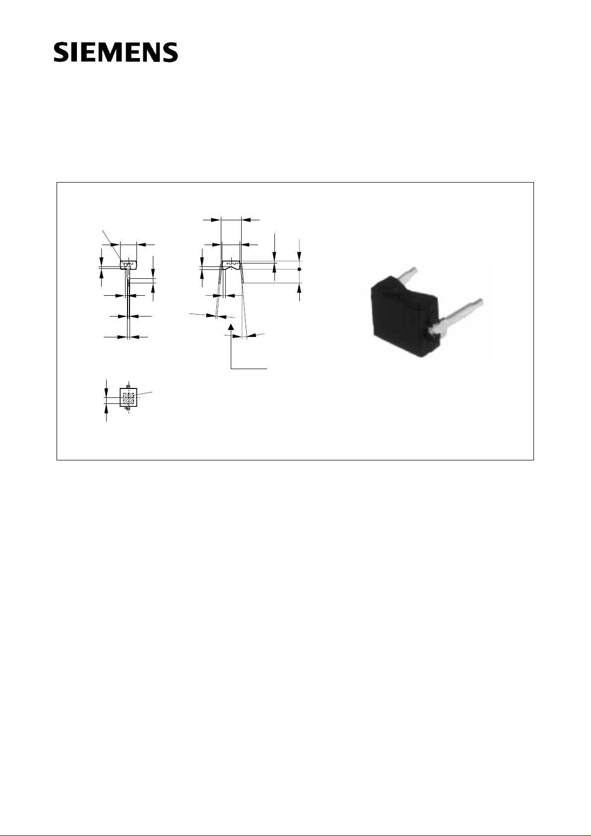
BPW 34 F
BPW 34 FS
BPW 34 FS (E9087)
5.4
Cathode marking
4.0
3.7
0.6
0.4
0.6
0.4
0.8
0.6
1.4
1.8
Approx. weight 0.1 g
Maße in mm, wenn nicht anders angegeben/Dimensions in mm, unless otherwise specified.
0.7
1.2
0.5
0.3
Photosensitive area
2.65 mm x 2.65 mm
0.35
0.2
Wesentliche Merkmale
● Speziell geeignet für Anwendungen
bei 950 nm
● kurze Schaltzeit (typ. 20 ns)
● DIL-Plastikbauform mit hoher
Packungsdichte
● BPW 34 FS/(E9087); geeignet für
0.8
0.6
4.9
4.5
4.3
0.6
0.4
0 ... 5˚
5.08 mm
spacing
Chip position
2.2
0.6
0.4
1.9
3.5
3.0
GEO06643
Features
● Especially suitable for applications
of 950 nm
● Short switching time (typ. 20 ns)
● DIL plastic package with high packing density
● BPW 34 FS/(E9087); suitable for vapor-
phase and IR-reflow soldering
BPW 34 F
Vapor-Phase Löten und IR-Reflow Löten
Anwendungen
● IR-Fernsteuerung von Fernseh- und
Rundfunkgeräten, Videorecordern,
Gerätefernsteuerungen
● Lichtschranken für Gleich- und
Applications
● IR remote control of hi-fi and TV sets,
video tape recorders, remote controls of
various equipment
● Photointerrupters
Wechsellichtbetrieb
feo06075
Semiconductor Group 1 1998-08-27
Page 2
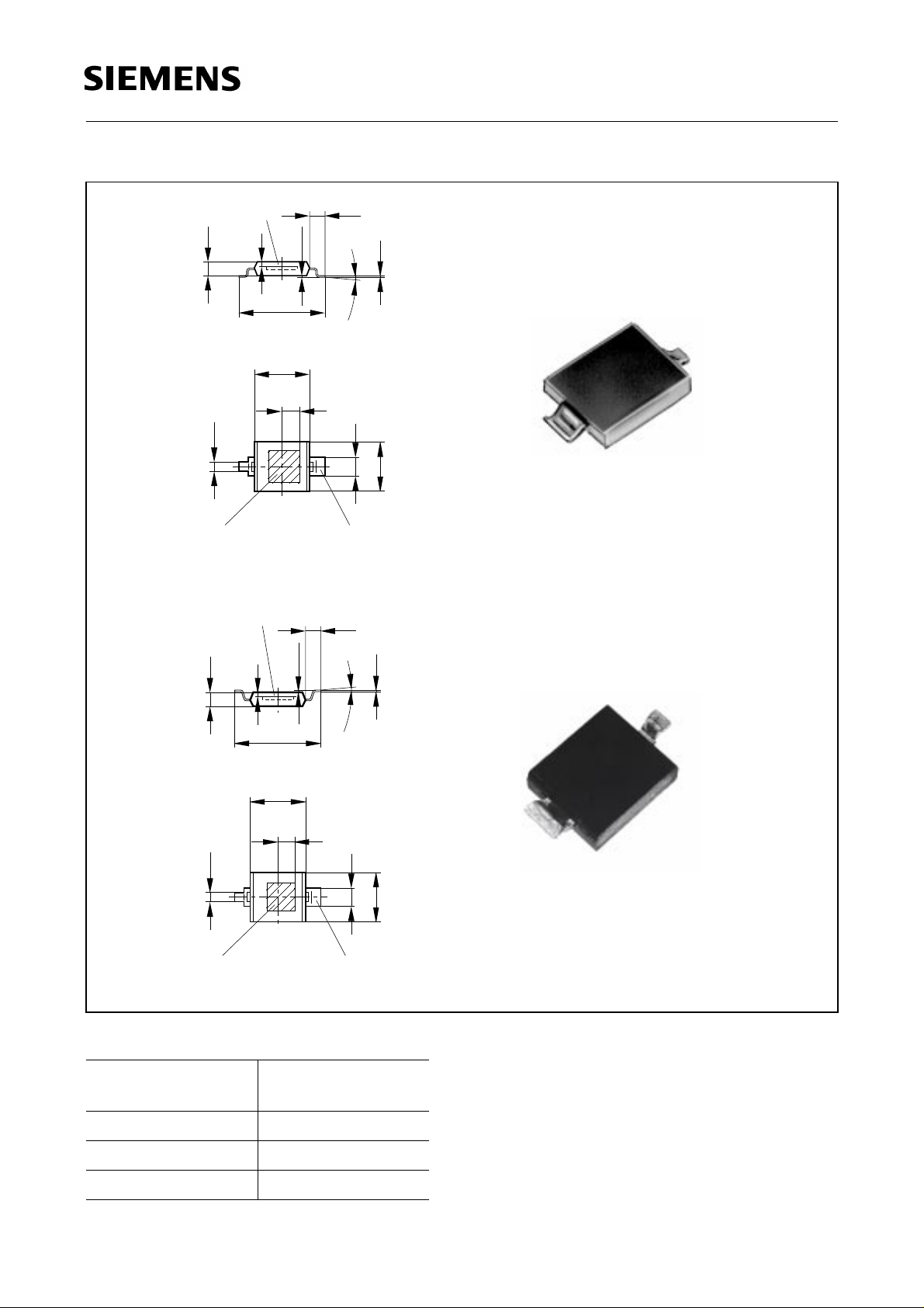
BPW 34 F, BPW 34 FS
BPW 34 FS (E9087)
0...0.1
1.1
0.9
0...5˚
1.5
1.7
GEO06863
1.1
0.9
0.2
4.0
0.1
3.7
Chip position
1.2
1.1
0.3
6.7
6.2
4.5
4.3
1.8
±0.2
0.9
0.7
Photosensitive area Cathode lead
2.65 mm x 2.65 mm
Chip position
feo06861feo06916
BPW 34 FS
0.2
1.7
0.1
1.5
1.2
0.9
1.1
0.7
0.3
6.7
6.2
4.5
4.3
1.8
0...0.1
0...5˚
±0.2
BPW 34 FAS (E9087)
4.0
3.7
Photosensitive area Cathode lead
2.65 mm x 2.65 mm
Maße in mm, wenn nicht anders angegeben/Dimensions in mm, unless otherwise specified.
Typ
Type
Bestellnummer
Ordering Code
GEO06916
BPW 34 F Q62702-P929
BPW 34 FS Q62702-P1604
BPW 34 FS (E9087) Q62702-P1826
Semiconductor Group 2 1998-08-27
Page 3

Grenzwerte
Maximum Ratings
BPW 34 F, BPW 34 FS
BPW 34 FS (E9087)
Bezeichnung
Description
Betriebs- und Lagertemperatur
Operating and storage temperature range
Sperrspannung
Reverse voltage
Verlustleistung, TA = 25 °C
Total power dissipation
Kennwerte (TA = 25 °C, λ = 950 nm)
Characteristics
Bezeichnung
Description
Fotoempfindlichkeit
Spectral sensitivity
V
= 5 V, Ee = 1 mW/cm
R
2
Wellenlänge der max. Fotoempfindlichkeit
Wavelength of max. sensitivity
Symbol
Symbol
T
; T
op
stg
V
R
P
tot
Symbol
Symbol
S
λ
S max
Wert
Value
Einheit
Unit
– 40 ... + 85 °C
32 V
150 mW
Wert
Value
Einheit
Unit
50 (≥ 40) µA
950 nm
Spektraler Bereich der Fotoempfindlichkeit
S = 10 % von S
max
Spectral range of sensitivity
S = 10 % of S
max
Bestrahlungsempfindliche Fläche
Radiant sensitive area
Abmessung der bestrahlungsempfindlichen
Fläche
Dimensions of radiant sensitive area
Halbwinkel
Half angle
Dunkelstrom, VR = 10 V
Dark current
Spektrale Fotoempfindlichkeit
Spectral sensitivity
Quantenausbeute
Quantum yield
Leerlaufspannung, Ee = 0.5 mW/cm
2
Open-circuit voltage
λ 780 ... 1100 nm
A 7.00 mm
L × B
L
× W
2.65 × 2.65 mm × mm
2
ϕ±60 Grad
deg.
I
R
S
λ
2 (≤ 30) nA
0.59 A/W
η 0.77 Electrons
Photon
V
O
330 (≥ 275) mV
Semiconductor Group 3 1998-08-27
Page 4

Kennwerte (TA = 25 °C, λ = 950 nm)
Characteristics (cont’d)
BPW 34 F, BPW 34 FS
BPW 34 FS (E9087)
Bezeichnung
Description
Kurzschlußstrom, Ee = 0.5 mW/cm
2
Short-circuit current
Anstiegs- und Abfallzeit des Fotostromes
Rise and fall time of the photocurrent
R
= 50 Ω; VR= 5 V; λ = 850 nm; Ip = 800 µA
L
Durchlaßspannung, IF= 100 mA, E = 0
Forward voltage
Kapazität, VR= 0 V, f = 1 MHz, E = 0
Capacitance
Temperaturkoeffizient von V
Temperature coefficient of V
Temperaturkoeffizient von I
Temperature coefficient of I
O
O
SC
SC
Rauschäquivalente Strahlungsleistung
Noise equivalent power
V
= 10 V
R
Nachweisgrenze, VR= 10 V
Detection limit
Symbol
Symbol
I
SC
t
, t
r
f
V
F
C
0
TC
V
TC
I
NEP
Wert
Value
25 µA
20 ns
1.3 V
72 pF
– 2.6 mV/K
0.18 %/K
4.3 × 10
D* 6.2 × 10
– 14
12
Einheit
Unit
W
√Hz
cm · √Hz
W
Semiconductor Group 4 1998-08-27
Page 5

BPW 34 F, BPW 34 FS
BPW 34 FS (E9087)
Relative spectral sensitivity
S
= f (λ)
rel
100
S
rel
%
80
60
40
20
0
700
800 900 1000 1200
Dark current
I
= f (VR), E = 0
R
4000
Ι
R
pA
3000
2000
1000
0
0 5 10 15 V 20
OHF00368
nm
λ
OHF00080
V
R
Photocurrent IP= f (Ee), VR = 5 V
Open-circuit voltage V
3
10
µ
AmV
Ι
P
2
10
1
10
0
10
-1
10
0
10
10110
O
V
O
Ι
P
2
= f (Ee)
µ
W/cm
OHF01097
2
10
E
e
10
10
10
10
10
4
Capacitance
C =f (V
C
), f = 1 MHz, E = 0
R
100
pF
80
OHF00081
Total power dissipation
P
= f (TA)
tot
4
3
2
1
0
160
mW
P
tot
140
120
100
80
60
40
20
0
0
Dark current
I
= f (TA), VR= 10 V, E = 0
R
3
10
nA
Ι
R
2
10
20 40 60 80 ˚C 100
70
60
50
10
1
40
30
10
0
20
10
-1
20 40 60 80 ˚C 100
0
10
0
-2
10
-1
10010
1
10210V
V
R
OHF00958
T
A
OHF00082
T
A
Directional characteristics S
40 30 20 10
50
60
70
80
90
100
rel
= f (ϕ)
0
ϕ
1.0
0.8
0.6
0.4
0.2
0
20 40 60 80 100 1200.40.60.81.0
0
OHF01402
Semiconductor Group 5 1998-08-27
 Loading...