

Page 1
Silizium-PIN-Fotodiode mit erhöhter Blauempfindlichkeit
Silicon PIN Photodiode with Enhanced Blue Sensitivity
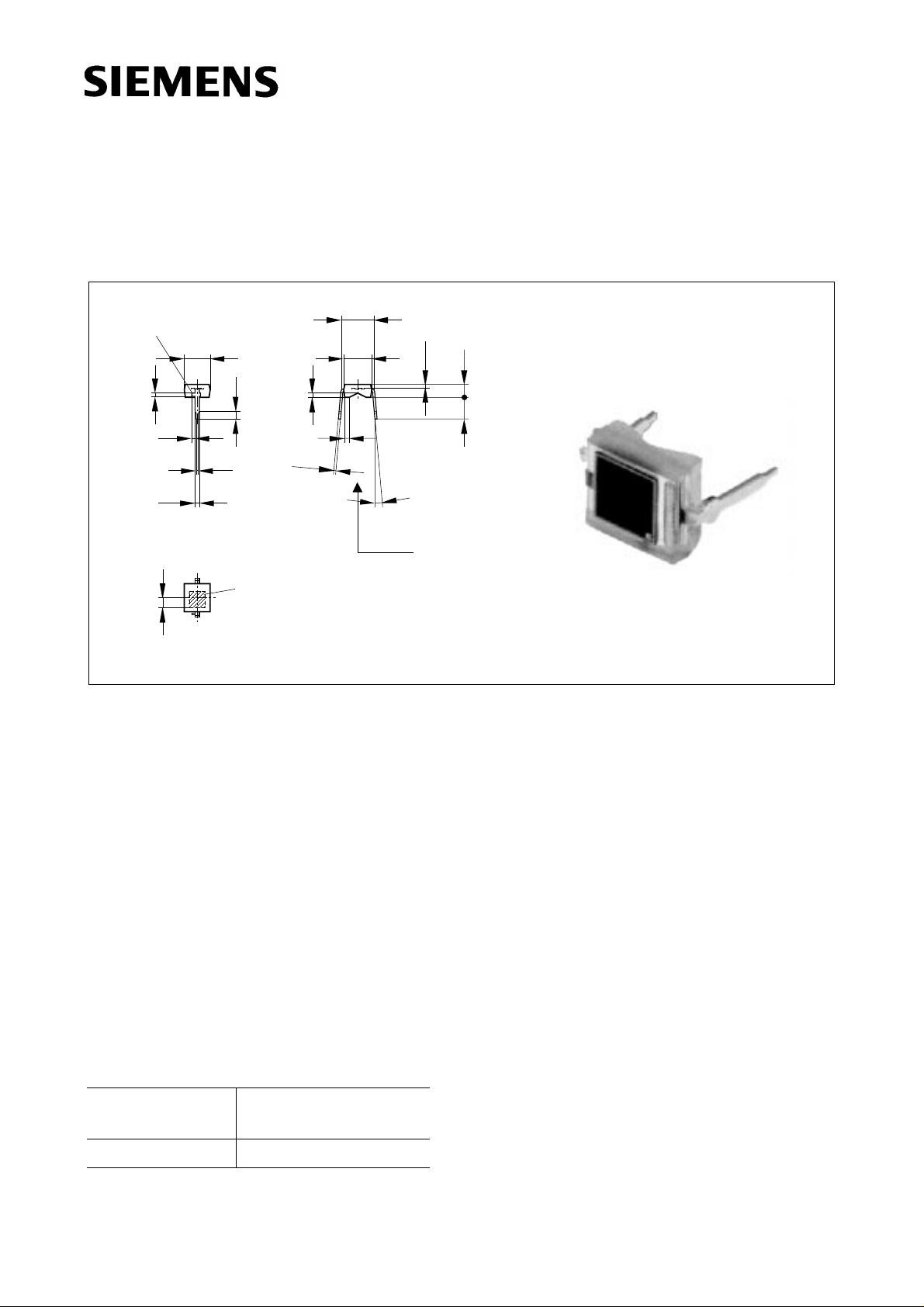
5.4
Cathode marking
4.0
3.7 4.3
0.6
1.8
0.4
0.6
0.4
0.8
0.6
1.4
1.2
0.5
0.3
Photosensitive area
2.65 mm x 2.65 mm
0.7
0.35
0.2
0.8
0.6
4.9
4.5
0.6
0.4
0 ... 5˚
5.08 mm
spacing
Chip position
2.2
0.6
0.4
1.9
3.5
3.0
BPW 34 B
Approx. weight 0.1 g
Maße in mm, wenn nicht anders angegeben/Dimensions in mm, unless otherwise specified
Wesentliche Merkmale
● Speziell geeignet für Anwendungen im
Bereich von 350 nm bis 1100 nm
● Kurze Schaltzeit (typ. 25 ns)
● DIL-Plastikbauform mit hoher
Packungsdichte
● SMT-Variante auf Anfrage
Anwendungen
● Lichtschranken für Gleich- und
Wechsellichtbetrieb im sichtbaren
Lichtbereich
● Industrieelektronik
● “Messen/Steuern/Regeln”
Typ
Type
Bestellnummer
Ordering Code
GEO06643
Features
● Especially suitable for applications from
350 nm to 1100 nm
● Short switching time (typ. 25 ns)
● DIL plastic package with high packing
density
● SMT version on request
Applications
● Photointerrupters
● Industrial electronics
● For control and drive circuits
feo06643
BPW 34 B Q62702-P945
Semiconductor Group 1 1997-11-19
Page 2
Grenzwerte
Maximum Ratings
BPW 34 B
Bezeichnung
Description
Betriebs- und Lagertemperatur
Symbol
Symbol
T
; T
op
stg
Operating and storage temperature range
Löttemperatur (Lötstelle 2 mm vom
Gehäuse entfernt bei Lötzeit
t ≤ 3 s)
T
S
Soldering temperature in 2 mm distance
from case bottom (t ≤ 3 s)
Sperrspannung
V
R
Reverse voltage
Verlustleistung,
= 25 °C
A
P
tot
T
Total power dissipation
Kennwerte (
T
= 25 °C, Normlicht A, T = 2856 K)
A
Characteristics (TA = 25 °C, standard light A, T = 2856 K)
Bezeichnung
Description
Symbol
Symbol
Wert
Value
Einheit
Unit
– 40 ... + 85 °C
230 °C
32 V
150 mW
Wert
Value
Einheit
Unit
V
Fotoempfindlichkeit,
= 5 V
R
Spectral sensitivity
Wellenlänge der max. Fotoempfindlichkeit
Wavelength of max. sensitivity
Spektraler Bereich der Fotoempfindlichkeit
S = 10 % von S
max
Spectral range of sensitivity
S = 10 % of S
max
Bestrahlungsempfindliche Fläche
Radiant sensitive area
Abmessung der bestrahlungsempfindlichen
Fläche
Dimensions of radiant sensitive area
Abstand Chipoberfläche zu Gehäuseoberfläche
Distance chip front to case surface
Halbwinkel
Half angle
Dunkelstrom, VR = 10 V
Dark current
S
λ
S max
75 nA/Ix
850 nm
λ 350 ... 1100 nm
A 7.45 mm
L × B
× W
L
H
ϕ±60 Grad
I
R
2.73 × 2.73 mm × mm
0.5 mm
deg.
2 (≤ 30) nA
2
Semiconductor Group 2 1997-11-19
Page 3

BPW 34 B
Kennwerte (
T
= 25 °C, Normlicht A, T = 2856 K)
A
Characteristics (TA = 25 °C, standard light A, T = 2856 K) (cont’d)
Bezeichnung
Description
Spektrale Fotoempfindlichkeit, λ = 400 nm
Symbol
Symbol
S
λ
Wert
Value
0.2 A/W
Spectral sensitivity
Quantenausbeute, λ = 400 nm
η 0.62
Quantum yield
Leerlaufspannung,
= 1000 Ix
v
V
O
390 mV
E
Open-circuit voltage
Kurzschlußstrom
I
SC
7.4 (≥ 5.4) µA
Short-circuit current
E
= 0.5 mW/cm2, λ = 400 nm
e
Anstiegs- und Abfallzeit des Fotostromes
t
, t
r
f
25 ns
Rise and fall time of the photocurrent
R
= 50 Ω; VR= 5 V; λ = 850 nm; Ip = 800 µA
L
Durchlaßspannung,
I
= 100 mA, E = 0
F
V
F
1.3 V
Forward voltage
Einheit
Unit
Electrons
Photon
Kapazität,
V
= 0 V, f = 1 MHz, E = 0
R
Capacitance
Temperaturkoeffizient von
Temperature coefficient of V
Temperaturkoeffizient von
Temperature coefficient of I
V
O
O
I
SC
SC
Rauschäquivalente Strahlungsleistung
Noise equivalent power
V
= 10 V, λ = 400 nm
R
Nachweisgrenze,
V
= 10 V, λ = 400 nm
R
Detection limit
C
0
TC
TC
NEP
V
I
72 pF
– 2.6 mV/K
0.18 %/K
1.3 × 10
D* 2.1 × 10
– 13
12
W
√Hz
cm · √Hz
W
Semiconductor Group 3 1997-11-19
Page 4

BPW 34 B
V
Relative spectral sensitivity
S
= f (λ)
rel
100
S
rel
%
80
60
40
20
0
400 600 800 1000 1200
Dark current
I
= f (VR), E = 0
R
4000
Ι
R
pA
3000
2000
1000
0
0 5 10 15 V 20
OHF01001
nm
λ
OHF00080
V
R
Photocurrent IP= f (Ev), VR = 5 V
Open-circuit voltage V
34
10
µ
AmV
Ι
P
2
10
1
10
0
10
-1
10
0
10
10110
= f (Ev)
O
OHF01066
10
10
V
O
Ι
P
10
10
2
103lx
10
4
10
E
V
Capacitance
C =f (V
C
), f = 1 MHz, E = 0
R
100
pF
80
OHF00081
Total power dissipation P
160
mW
P
tot
140
3
2
1
0
120
100
80
60
40
20
0
0
Dark current
IR= f (TA), VR= 5 V, E = 0
3
10
nA
Ι
R
2
10
= f (TA)
tot
20 40 60 80 ˚C 100
OHF00082
70
60
50
10
1
40
30
10
0
20
10
-1
0
20 40 60 80 ˚C 100
T
10
0
10
-1
-2
10010110210V
V
R
OHF00958
T
A
A
Directional characteristics S
40 30 20 10
50
60
rel
= f (ϕ)
0
ϕ
1.0
0.8
0.6
OHF01402
70
80
90
100
0.4
0.2
0
20 40 60 80 100 1200.40.60.81.0
0
Semiconductor Group 4 1997-11-19
 Loading...