

Page 1

DISCRETE SEMICONDUCTORS
DATA SH EET
BF689K
NPN 2 GHz wideband transistor
Product specification
File under Discrete Semiconductors, SC14
September 1995
Page 2
Philips Semiconductors Product specification
NPN 2 GHz wideband transistor BF689K
DESCRIPTION
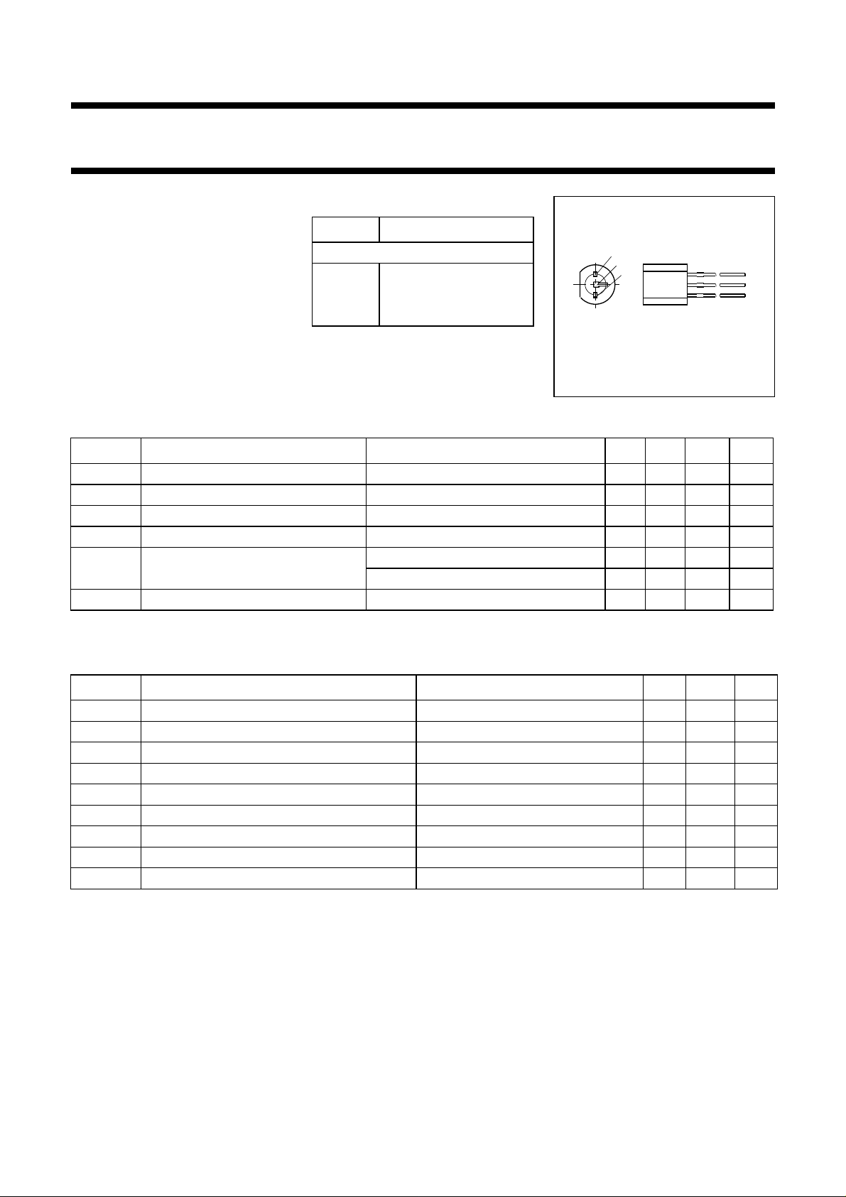
NPN transistor in a plastic SOT54
(TO-92 variant) envelope. It is
intended for application as an
amplifier or oscillator in the VHF and
UHF range.
PINNING
PIN DESCRIPTION
Code: F689
1 emitter
2 base
3 collector
1
2
3
MSB034
Fig.1 SOT54.
QUICK REFERENCE DATA
SYMBOL PARAMETER CONDITIONS MIN. TYP. MAX. UNIT
V
CBO
V
CEO
I
C
P
tot
h
FE
f
T
collector-base voltage open emitter −−25 V
collector-emitter voltage open base −−15 V
DC collector current −−25 mA
total power dissipation up to T
= 60 °C −−360 mW
amb
DC current gain IC = 2 mA; VCE = 5 V; Tj = 25 °C20−−
I
= 20 mA; VCE = 5 V; Tj = 25 °C35−−
C
transition frequency IC = 15 mA; VCE = 5 V; f = 500 MHz − 1.8 − GHz
LIMITING VALUES
In accordance with the Absolute Maximum System (IEC 134).
SYMBOL PARAMETER CONDITIONS MIN. MAX. UNIT
V
V
V
V
I
I
P
T
T
CBO
CEO
CER
EBO
C
CM
tot
stg
j
collector-base voltage open emitter − 25 V
collector-emitter voltage open base − 15 V
collector-emitter voltage RBE≤ 50 Ω−25 V
emitter-base voltage open collector − 3.5 V
DC collector current − 25 mA
peak collector current tp< 1 µs − 50 mA
total power dissipation up to T
= 60 °C − 360 mW
amb
storage temperature −55 150 °C
junction temperature − 150 °C
September 1995 2
Page 3
Philips Semiconductors Product specification
NPN 2 GHz wideband transistor BF689K
THERMAL RESISTANCE
SYMBOL PARAMETER CONDITIONS THERMAL RESISTANCE
R
th j-a
CHARACTERISTICS
= 25 °C unless otherwise specified.
T
j
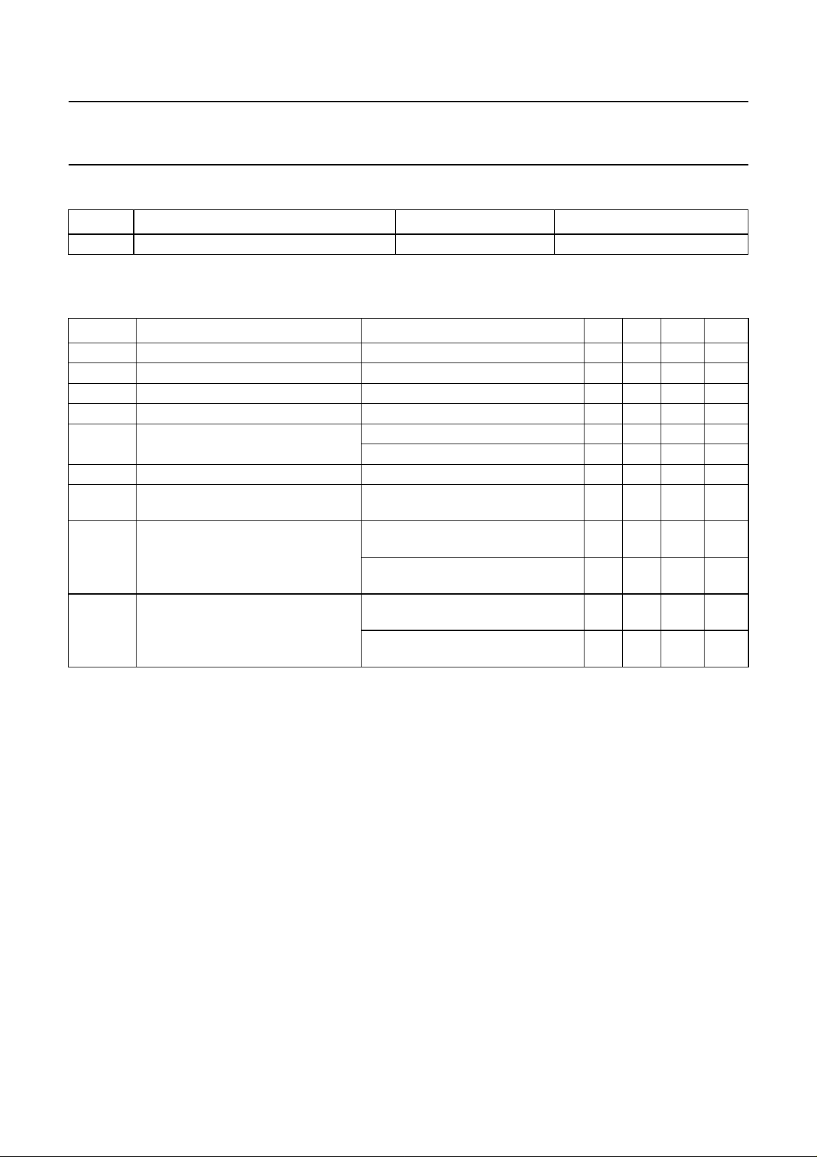
SYMBOL PARAMETER CONDITIONS MIN. TYP. MAX. UNIT
I
CBO
I
EBO
V
CE sat
V
BE sat
h
FE
f
T
C
re
G
p
F noise figure I
thermal resistance from junction to ambient in free air 250 K/W
collector cut-off current IE = 0; VCB = 15 V −−50 nA
emitter cut-off current IC = 0; VEB = 2 V −−1 µA
collector-emitter saturation voltage IC = 25 mA; IB = 1.25 mA −−1.0 V
base-emitter saturation voltage IC = 25 mA; IB = 1.25 mA −−1.0 V
DC current gain IC = 2 mA; VCE = 5 V 20 −−
I
= 20 mA; VCE = 5 V 35 −−
C
transition frequency IC = 15 mA; VCE = 5 V; f = 500 MHz − 1.8 − GHz
feedback capacitance IC= 2 mA; VCE = 5 V; f = 1 MHz;
T
= 25 °C
amb
power gain IC = 2 mA; VCE = 5 V; f = 100 MHz;
T
= 25 °C; ZS = 60 Ω;RL = 2 kΩ
amb
I
= 2 mA; VCE = 5 V; f = 200 MHz;
C
T
= 25 °C; ZS = 60 Ω;RL = 920 Ω
amb
= 2 mA; VCE = 5 V; f = 100 MHz;
C
T
= 25 °C; ZS = 60 Ω
amb
I
= 2 mA; VCE = 5 V; f = 200 MHz;
C
T
= 25 °C; ZS = 60 Ω
amb
− 1.1 − pF
− 16 − dB
− 16 − dB
− 4 − dB
− 3 − dB
September 1995 3
Page 4
Philips Semiconductors Product specification
NPN 2 GHz wideband transistor BF689K
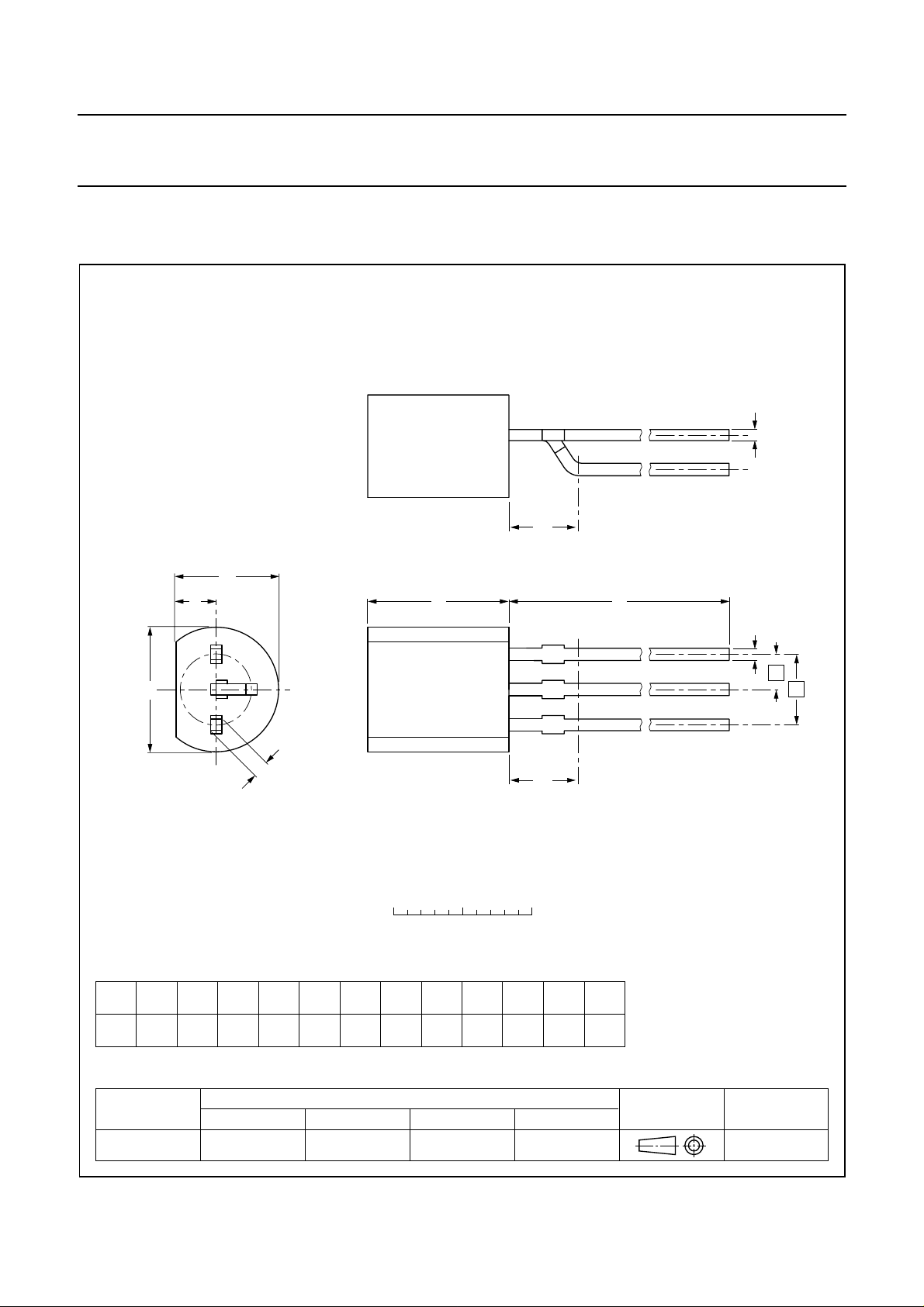
PACKAGE OUTLINE
Plastic single-ended leaded (through hole) package; 3 leads (on-circle) SOT54 variant
c
L
2
E
d
A L
1
2
D
3
b
1
0 2.5 5 mm
scale
DIMENSIONS (mm are the original dimensions)
UNIT
Notes
1. Terminal dimensions within this zone are uncontrolled to allow for flow of plastic and terminal irregularities.
A
b
5.2
0.48
mm
5.0
OUTLINE
VERSION
SOT54 variant TO-92 SC-43
0.40
0.66
0.56
c
D
d
E
4.2
3.6
e
2.54
b
1
0.45
4.8
4.4
1.7
1.4
REFERENCES
0.40
IEC JEDEC EIAJ
e
1.27
1
L
14.5
12.7
L
1
L
1
max
2.5 2.5
(1)
L
2
max
EUROPEAN
PROJECTION
b
e
1
e
ISSUE DATE
97-04-14
September 1995 4
Page 5

Philips Semiconductors Product specification
NPN 2 GHz wideband transistor BF689K
DEFINITIONS
Data Sheet Status
Objective specification This data sheet contains target or goal specifications for product development.
Preliminary specification This data sheet contains preliminary data; supplementary data may be published later.
Product specification This data sheet contains final product specifications.
Limiting values
Limiting values given are in accordance with the Absolute Maximum Rating System (IEC 134). Stress above one or
more of the limiting values may cause permanent damage to the device. These are stress ratings only and operation
of the device at these or at any other conditions above those given in the Characteristics sections of the specification
is not implied. Exposure to limiting values for extended periods may affect device reliability.
Application information
Where application information is given, it is advisory and does not form part of the specification.
LIFE SUPPORT APPLICATIONS
These products are not designed for use in life support appliances, devices, or systems where malfunction of these
products can reasonably be expected to result in personal injury. Philips customers using or selling these products for
use in such applications do so at their own risk and agree to fully indemnify Philips for any damages resulting from such
improper use or sale.
September 1995 5
 Loading...