

Page 1

DISCRETE SEMICONDUCTORS
DATA SH EET
BF410A to D
N-channel silicon field-effect
transistors
Product specification
File under Discrete Semiconductors, SC07
December 1990
Page 2
Philips Semiconductors Product specification
N-channel silicon field-effect transistors BF410A to D
DESCRIPTION
Asymmetrical N-channel planar
epitaxial junction field-effect
transistors in a plastic TO-92 variant;
intended for applications up to the
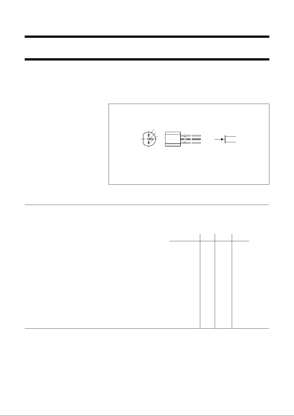
PINNING - TO-92 VARIANT
1 = drain
2 = source
3 = gate
VHF range.
These FETs can be supplied in four
I
groups. Special features are the
DSS
low feedback capacitance and the low
noise figure. Thanks to these special
handbook, halfpage
features the BF410 is very suitable for
applications such as the RF stages in
FM portables (type A), car radios
(type B) and mains radios (type C) or
the mixer stage (type D).
QUICK REFERENCE DATA
Drain-source voltage V
Drain current (DC or average) I
Total power dissipation
up to T
=75°CP
amb
Drain current
V
= 10 V; VGS=0
DS
Transfer admittance
V
= 10 V; VGS= 0; f = 1 kHz yfs min. 2.5 4 6 7 mS
DS
Feedback capacitance
VDS= 10 V; VGS=0 C
V
= 10 V; ID= 5 mA C
DS
Noise figure at optimum source admittance
G
= 1 mS; −BS= 3 mS; f = 100 MHz
S
V
= 10 V; VGS= 0 F typ. 1.5 1.5 −−dB
DS
V
= 10 V; ID= 5 mA F typ. −− 1.5 1.5 dB
DS
1
2
3
g
MAM257
Fig.1 Simplified outline and symbol
DS
D
tot
max. 20 V
max. 30 mA
max. 300 mW
BF410A B C D
I
DSS
rs
rs
min. 0.7 2.5 6 10 mA
max. 3.0 7.0 12 18 mA
typ. 0.5 0.5 −−pF
typ. −− 0.5 0.5 pF
d
s
December 1990 2
Page 3

Philips Semiconductors Product specification
N-channel silicon field-effect transistors BF410A to D
RATINGS
Limiting values in accordance with the Absolute Maximum System (IEC 134)
Drain-source voltage V
Drain-gate voltage (open source) V
Drain current (DC or average) I
Gate current ± I
Total power dissipation up to T
=75°CP
amb
Storage temperature range T
Junction temperature T
THERMAL RESISTANCE
DS
DGO
D
G
tot
stg
j
max. 20 V
max. 20 V
max. 30 mA
max. 10 mA
max. 300 mW
−65 to +150 °C
max. 150 °C
From junction to ambient in free air R
th j-a
= 250 K/W
STATIC CHARACTERISTICS
=25°C
T
amb
Gate cut-off current BF410A B C D
= 0.2 V; VDS=0 −I
−V
GS
GSS
max. 10 10 10 10 nA
Gate-drain breakdown voltage
I
=0;−ID=10µA −V
S
(BR)GDO
min. 20 20 20 20 V
Drain current
V
= 10 V; VGS=0
DS
I
DSS
min. 0.7 2.5 6 10 mA
max. 3.0 7.0 12 18 mA
Gate-source cut-off voltage
I
=10µA; VDS= 10 V −V
D
(P)GS
typ. 0.8 1.5 2.2 3 V
December 1990 3
Page 4

Philips Semiconductors Product specification
N-channel silicon field-effect transistors BF410A to D
DYNAMIC CHARACTERISTICS
Measuring conditions (common source): V
=10V; VGS= 0; T
DS
=10V; ID= 5 mA; T
V
DS
=25°C for BF410A and B
amb
=25°C for BF410C and D
amb
y-parameters (common source) BF410A B C D
Input capacitance at f = 1 MHz C
Input conductance at f = 100 MHz g
Feedback capacitance at f = 1 MHz C
is
is
rs
Transfer admittance at f = 1 kHz y
V
= 0 instead of ID=5mA yfs min. −−6.0 7.0 mS
GS
Transfer admittance at f = 100 MHz y
Output capacitance at f = 1 MHz C
Output conductance at f = 1 MHz g
Output conductance at f = 100 MHz g
os
os
os
max. 5 5 5 5 pF
typ. 100 90 60 50 µS
typ. 0.5 0.5 0.5 0.5 pF
max. 0.7 0.7 0.7 0.7 pF
min. 2.5 4.0 4.0 3.5 mS
fs
typ. 3.5 5.5 5.0 5.0 mS
fs
max. 3 3 3 3 pF
max. 60 80 100 120 µS
typ. 35 55 70 90 µS
Noise figure at optimum source admittance
G
= 1 mS; −BS= 3 mS; f = 100 MHz F typ. 1.5 1.5 1.5 1.5 dB
S
1.5
handbook, halfpage
C
rs
(pF)
1
MDA277
10
handbook, halfpage
|y
|
fs
(mA/V)
8
6
BF410A
BF410B
BF410C
MDA278
BF410D
0.5
typ
0
0
4 8 12 16
VDS (V)
20
Fig.2 VGS= 0 for BF410A and BF410B;
ID= 5 mA for BF410C and BF410D;
f = 1 MHz; T
amb
=25°C.
December 1990 4
4
2
0
05
Fig.3 VDS10 V; f = 1 kHz; T
10 15
ID (mA)
=25°C; typical values.
amb
Page 5

Philips Semiconductors Product specification
N-channel silicon field-effect transistors BF410A to D
PACKAGE OUTLINE
Plastic single-ended leaded (through hole) package; 3 leads (on-circle) SOT54 variant
c
L
2
E
d
A L
1
2
D
3
b
1
0 2.5 5 mm
scale
DIMENSIONS (mm are the original dimensions)
UNIT
Notes
1. Terminal dimensions within this zone are uncontrolled to allow for flow of plastic and terminal irregularities.
A
b
5.2
0.48
mm
5.0
OUTLINE
VERSION
SOT54 variant TO-92 SC-43
0.40
0.66
0.56
c
D
d
E
4.2
3.6
e
2.54
b
1
0.45
4.8
4.4
1.7
1.4
REFERENCES
0.40
IEC JEDEC EIAJ
e
1.27
1
L
14.5
12.7
L
1
L
1
max
2.5 2.5
(1)
L
2
max
EUROPEAN
PROJECTION
b
e
1
e
ISSUE DATE
97-04-14
December 1990 5
Page 6

Philips Semiconductors Product specification
N-channel silicon field-effect transistors BF410A to D
DEFINITIONS
Data sheet status
Objective specification This data sheet contains target or goal specifications for product development.
Preliminary specification This data sheet contains preliminary data; supplementary data may be published later.
Product specification This data sheet contains final product specifications.
Short-form specification The data in this specification is extracted from a full data sheet with the same type
number and title. For detailed information see the relevant data sheet or data handbook.
Limiting values
Limiting values given are in accordance with the Absolute Maximum Rating System (IEC 134). Stress above one or
more of the limiting values may cause permanent damage to the device. These are stress ratings only and operation
of the device at these or at any other conditions above those given in the Characteristics sections of the specification
is not implied. Exposure to limiting values for extended periods may affect device reliability.
Application information
Where application information is given, it is advisory and does not form part of the specification.
LIFE SUPPORT APPLICATIONS
These products are not designed for use in life support appliances, devices, or systems where malfunction of these
products can reasonably be expected to result in personal injury. Philips customers using or selling these products for
use in such applications do so at their own risk and agree to fully indemnify Philips for any damages resulting from such
improper use or sale.
December 1990 6
 Loading...