

Page 1
SILICON PNP POWER DARLINGTON TRANSISTOR
■ SGS-THOMS O N PREF ERRE D SA LES TYP E
■ PNP DARLING TO N
■ INTEGRATED ANTIPARALLEL
COLLECTOR-EMITTER DIODE
APPLICATIONS
■ GENERAL PURPOSE SWITCHING
■ GENER AL PURPO SE AMPLIFIERS
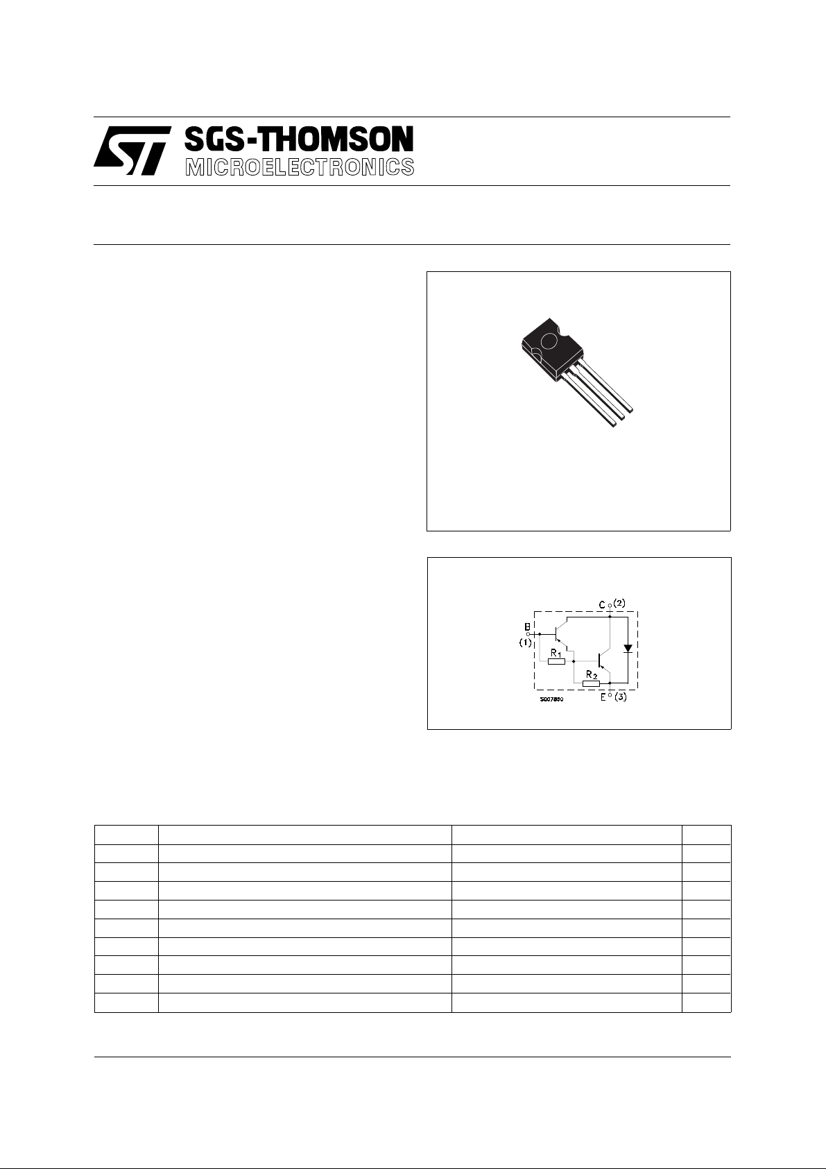
BD336
DESCRIPTION
The BD336 is a silicon epitaxial-base PNP
transistor in Darlingon configuration mounted in
SOT-82 plastic package.
It is inteded for use in audio output stages
general amplifier and switching applications.
ABSOL UT E MAXIMU M RATINGS
3
2
1
SOT-82
INTERNAL SCHEMATIC DIAGRAM
Symbol Parameter Value Unit
V
V
V
I
P
T
Collector-Base Voltage (IE = 0) -100 V
CBO
Collector-Emitter Voltage (IB = 0) -100 V
CEO
Emitter-Base Voltage (IC = 0) -5 V
EBO
Collector Current -6 A
I
C
Collector Peak Current (tp < 10ms) -10 A
CM
Base Current -0.15 A
I
B
Total Dissipation at Tc ≤ 25 oC60W
tot
Storage Temperature -65 to 150
stg
Max. Operating Junction Temperature 150
T
j
July 1997
o
C
o
C
1/4
Page 2

BD336
THERMAL DATA
R
thj-case
Thermal Resistance Junction-case Max 2.08
o
C/W
ELECTRICAL CHARACTERISTICS (T
= 25 oC unless otherwise specified)
case
Symbol Parameter Test Conditions Min. Typ. Max. Unit
I
I
I
V
CE(sat)
CBO
CEO
EBO
Collector Cut-off
Current (I
= 0)
E
Collector Cut-off
Current (I
= 0)
B
Emitter Cut-off Current
(I
= 0)
C
∗ Collector-Emitter
= -100 V
V
CB
V
= -100 V TC = 150 oC
CB
= -50 V -0.5 mA
V
CE
= -5 V -5 mA
V
EB
-0.2-2mA
IC = -3 A IB = -12 mA -2 V
Saturation Voltage
∗ Base-Emitter Voltage IC = -3 A VCE = -3 V -2.5 V
V
BE
h
∗ DC Current Gain IC = -0.5 A VCE = -3 V
FE
V
∗ Parallel Diode Forward
F
I
= -3 A VCE = -3 V
C
I
= -6 A VCE = -3 V
C
IF = -3 A -1.8 V
750
2700
400
Voltage
h
Small Signal Current
fe
IC = -3 A VCE = -3 V f = 1MHz 150
Gain
t
t
∗ Pulsed: Pulse duration = 300 µs, duty cycle ≤ 1.5 %
Turn on Time IC = -3 A VCC = -30 V
on
Turn off Time 5 10 µ s
off
I
= -IB2 = -12 mA
B1
12µs
mA
2/4
Page 3

P032A
SOT-82 MECHANICAL DATA
BD336
DIM.
MIN. TYP. MAX. MIN. TYP. MAX.
A 7.4 7.8 0.291 0.307
B 10.5 10.8 0.413 0.444
b 0.7 0.9 0.028 0.035
b1 0.49 0.75 0.019 0.030
C 2.4 2.7 0.04 0.106
c1 1.0 1.3 0.039 0.05
D 15.4 16 0.606 0.629
e 2.2 0.087
e3 4.15 4.65 0.163 0.183
F 3.8 0.150
H 2.54 0.100
H2 2.15 0.084
mm inch
C
A
F
B
H2
H
D
c1
b
b1
e
e3
3/4
Page 4

BD336
Information furnished is believed to be accurate and reliable. However, SGS-THOMSON Microelectronics assumes no responsability for the
consequences of use of such information nor for any infringement of patents or other rights of third parties which may results from its use. No
license is granted by implication or ot h erwise under any patent or patent rights of SGS-THOMSON Microelectronics. Specifi cations mentioned
in this publication are subject to change without notice. This publication sup ersedes and replaces all information previously supplied.
SGS-THOMSON Microelectronics products are not authorized for use as critical components in life support devices or systems without express
written approval of SGS-THOMSON Microelectonics.
© 1997 SGS-THOMSON Microelectronics - Printed in Italy - All Rights Reserved
Australia - Brazil - Canada - China - France - Germany - Hong Kong - Italy - Japan - Korea - Malaysia - Malta - Morocco - The Netherlands -
Singapore - Spain - Sweden - Switzerland - Taiwan - Thailand - United Kingdom - U.S.A
SGS-THOMSON Microelectronics GROUP OF COMPANIES
. . .
4/4
 Loading...