

Page 1
PNP Silicon AF Transistors BCW 67
BCW 68
● For general AF applications
● High current gain
● Low collector-emitter saturation voltage
● Complementary types: BCW 65, BCW 66 (NPN)
Type Ordering Code
Marking
(tape and reel)
BCW 67 A
BCW 67 B
BCW 67 C
BCW 68 F
BCW 68 G
BCW 68 H
DAs
DBs
DCs
DFs
DGs
DHs
Q62702-C1560
Q62702-C1480
Q62702-C1681
Q62702-C1893
Q62702-C1322
Q62702-C1555
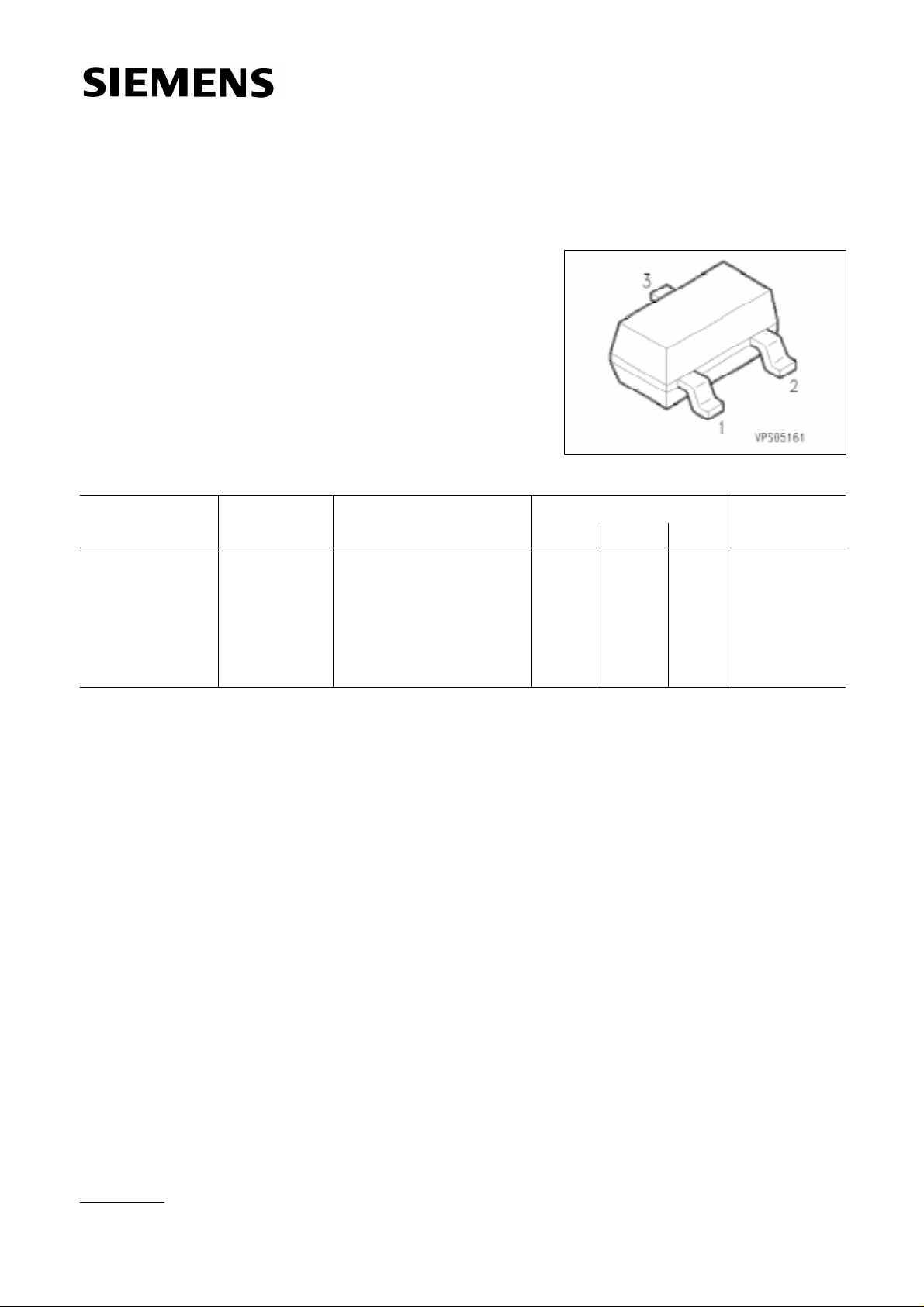
Pin Configuration
1 2 3
B E C
Package
SOT-23
1)
1)
For detailed information see chapter Package Outlines.
Semiconductor Group 1
5.91
Page 2
BCW 67
BCW 68
Maximum Ratings
Parameter Symbol Values Unit
BCW 67 BCW 68
Collector-emitter voltage V
Collector-base voltage VCB0
Emitter-base voltage V
Collector current I
Peak collector current ICM A
CE0 V
32 45
45 60
EB0
C mA
55
800
1
Base current IB mA100
Peak base current I
Total power dissipation, T
S = 79 ˚C Ptot mW
Junction temperature Tj ˚C
Storage temperature range T
BM 200
330
150
stg
– 65 … + 150
Thermal Resistance
Junction - ambient
1)
Rth JA ≤ 285 K/W
Junction - soldering point Rth JS ≤ 215
1)
Package mounted on epoxy pcb 40 mm × 40 mm × 1.5 mm/6 cm2 Cu.
Semiconductor Group 2
Page 3

Electrical Characteristics
I
I
I
I
I
I
A = 25 ˚C, unless otherwise specified.
at T
DC characteristics
BCW 67
BCW 68
UnitValuesParameter Symbol
min. typ. max.
VCollector-emitter breakdown voltage
C = 10 mA
BCW 67
BCW 68
Collector-base breakdown voltage
C = 10 µA
BCW 67
BCW 68
(BR)CE0
V
(BR)CB0
V
32
45
45
60
–
–
–
–
–
–
–
–
Emitter-base breakdown voltage, IE = 10 µA V(BR)EB0 5––
Collector cutoff current
VCB = 32 V BCW 67
CB = 45 V BCW 68
V
CB = 32 V, TA = 150 ˚C BCW 67
V
CB = 45 V, TA = 150 ˚C BCW 68
V
EB = 4 V IEB0 ––20
DC current gain
C = 100 µA, VCE = 10 V
1)
BCW 67 A, BCW 68 F
BCW 67 B, BCW 68 G
BCW 67 C, BCW 68 H
C = 10 mA, VCE = 1 V
BCW 67 A, BCW 68 F
BCW 67 B, BCW 68 G
BCW 67 C, BCW 68 H
C = 100 mA, VCE = 1 V
BCW 67 A, BCW 68 F
BCW 67 B, BCW 68 G
BCW 67 C, BCW 68 H
C = 500 mA, VCE = 2 V
BCW 67 A, BCW 68 F
BCW 67 B, BCW 68 G
BCW 67 C, BCW 68 H
I
h
CB0
FE
–
–
–
–
35
50
80
75
120
180
100
160
250
35
60
100
–
–
–
–
–
–
–
–
–
–
160
250
350
–
–
–
20
20
20
20
–
–
–
–
–
–
250
400
630
–
–
–
nA
nA
µA
µA
nAEmitter-base cutoff current, V
–
1)
Pulse test: t ≤ 300 µs, D = 2 %.
Semiconductor Group 3
Page 4

Electrical Characteristics
I
I
I
I
I
A = 25 ˚C, unless otherwise specified.
at T
DC characteristics
BCW 67
BCW 68
UnitValuesParameter Symbol
min. typ. max.
Collector-emitter saturation voltage
C = 100 mA, IB = 10 mA
C = 500 mA, IB = 50 mA
Base-emitter saturation voltage
C = 100 mA, IB = 10 mA
C = 500 mA, IB = 50 mA
1)
AC characteristics
C = 50 mA, VCE = 5 V, f = 20 MHz
CB = 10 V, f = 1 MHz
V
Input capacitance
EB = 0.5 V, f = 1 MHz
V
1)
V
CEsat
–
–
V
BEsat
–
–
f
T – 200 –
C
obo –6–
C
ibo –60–
–
–
–
–
0.3
0.7
1.25
2
V
MHzTransition frequency
pFOutput capacitance
1)
Pulse test: t ≤ 300 µs, D = 2 %.
Semiconductor Group 4
Page 5

BCW 67
BCW 68
Total power dissipation Ptot = f (TA*; TS)
* Package mounted on epoxy
Transition frequency fT = f (IC)
CE = 5 V
V
Permissible pulse load P
tot max/Ptot DC = f (tp)
Collector cutoff current I
CB = VCEmax
V
CB0 = f (TA)
Semiconductor Group 5
Page 6

BCW 67
BCW 68
Base-emitter saturation voltage
C = f (VBEsat)
I
FE = 10
h
Collector-emitter saturation voltage
C = f (VCEsat)
I
FE = 10
h
DC current gain hFE = f (IC)
CE = 1 V
V
Semiconductor Group 6
 Loading...