

Page 1
PNP Silicon Double Transistor
g
• To be used as a current mirror
BCV62
• Good thermal coupling and V
• High current gain
matching
BE
3
4
• Low collector-emitter saturation voltage
• Pb-free (RoHS compliant) package
• Qualified according AEC Q101
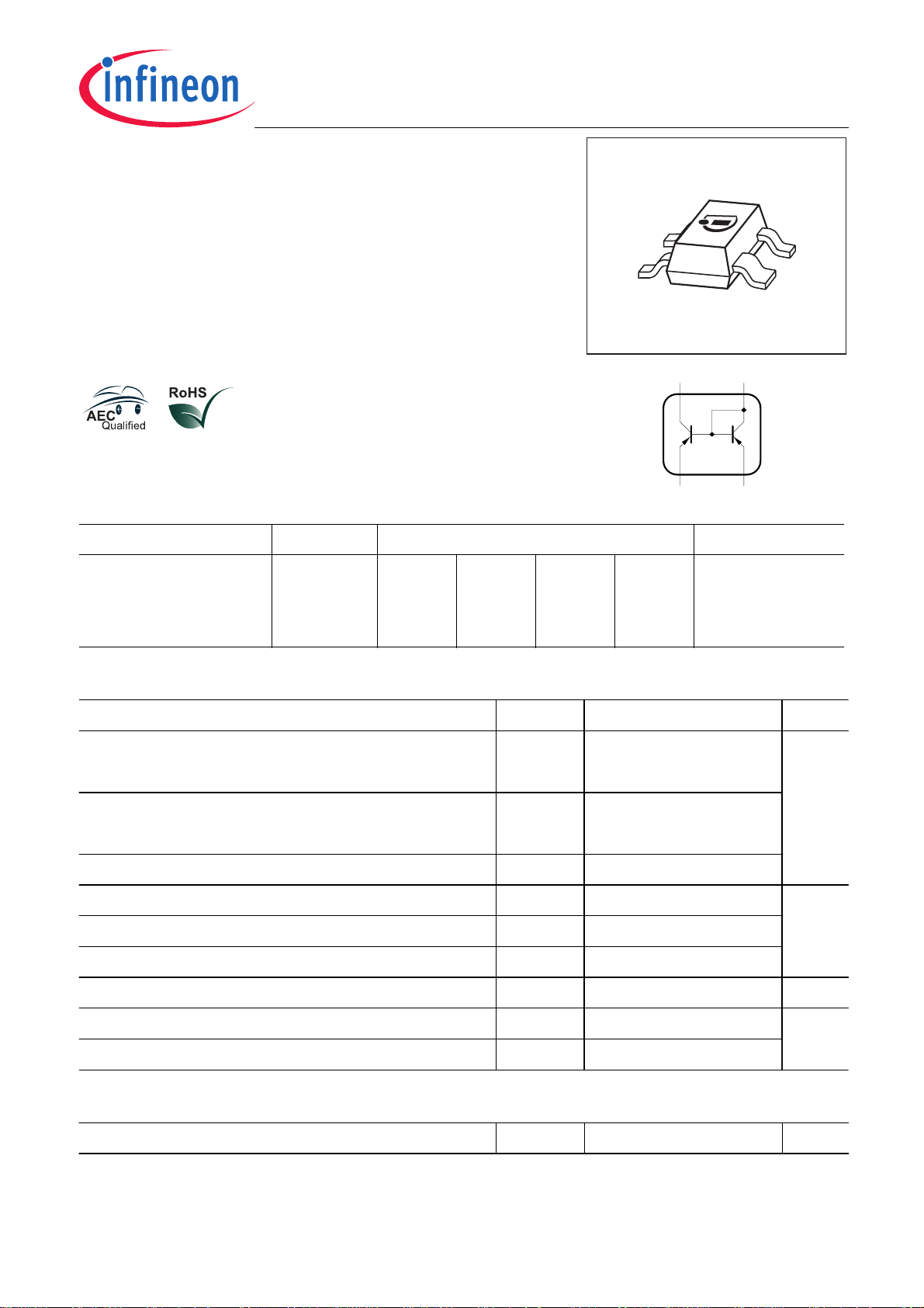
C1 (2)
E1 (3) E2 (4)
C2 (1)
Tr.2Tr.1
EHA00013
Type Marking Pin Configuration Package
BCV62A
BCV62B
BCV62C
3Js
3Ks
3Ls
1 = C2
1 = C2
1 = C2
2 = C1
2 = C1
2 = C1
3 = E1
3 = E1
3 = E1
4 = E2
4 = E2
4 = E2
SOT143
SOT143
SOT143
Maximum Ratings
2
1
Parameter
Collector-emitter voltage
Symbol Value Unit
V
(transistor T1)
Collector-base voltage (open emitter)
V
(transistor T1)
Emitter-base voltage V
DC collector current I
Peak collector current I
Base peak current (transistor T1) I
Total power dissipation, TS = 99 °C P
Junction temperature T
Storage temperature T
Thermal Resistance
Junction - soldering point
1)
R
CEO
CBO
EBS
C
CM
BM
tot
j
st
thJS
30 V
30
6
100 mA
200
200
300 mW
150 °C
-65 ... 150
≤170 K/W
1
For calculation of R
please refer to Application Note AN077 (Thermal Resistance Calculation)
thJA
1
2011-07-25
Page 2

Electrical Characteristics at TA = 25°C, unless otherwise specified
BCV62
Parameter
DC Characteristics of T1
Collector-emitter breakdown voltage
= 10 mA, IB = 0
I
C
Collector-base breakdown voltage
= 10 µA, IE = 0
I
C
Emitter-base breakdown voltage
= 10 µA, IC = 0
I
E
Collector cutoff current
= 30 V, IE = 0
V
CB
Collector cutoff current
= 30 V, IE = 0 , TA = 150 °C
V
CB
DC current gain 1)
= 0.1 mA, VCE = 5 V
I
C
Symbol Values Unit
min. typ. max.
V
(BR)CEO
V
(BR)CBO
V
(BR)EBO
I
CBO
I
CBO
h
FE
30 - - V
30 - -
6 - -
- - 15 nA
- - 5 µA
100 - -
-
DC current gain 1)
= 2 mA, VCE = 5 V
I
C
Collector-emitter saturation voltage1)
= 10 mA, IB = 0.5 mA
I
C
= 100 mA, IB = 5 mA
I
C
Base-emitter saturation voltage 1)
= 10 mA, IB = 0.5 mA
I
C
= 100 mA, IB = 5 mA
I
C
Base-emitter voltage 1)
= 2 mA, VCE = 5 V
I
C
= 10 mA, VCE = 5 V
I
C
1) Pulse test: t ≤ 300µs, D = 2%
BCV62A
BCV62B
BCV62C
h
FE
V
CEsat
V
BEsat
V
BE(ON)
125
220
420
-
-
-
-
600
-
180
290
520
75
250
700
850
650
-
220
475
800
300
650
-
-
750
820
mV
2
2011-07-25
Page 3

Electrical Characteristics at TA = 25°C, unless otherwise specified.
BCV62
Parameter
DC Characteristics
Base-emitter forward voltage
I
= 10 µA
E
= 250 mA
I
E
Matching of transistor T1 and transistor T2
at I
= 0.5mA and V
E2
= 25 °C
T
A
= 150 °C
T
A
CE1
= 5V
Thermal coupling of transistor T1 and
1)
transistor T2
Maximum current of thermal stability of I
T1: VCE = 5V
C1
AC characteristics of transistor T1
Transition frequency
I
= 10 mA, VCE = 5 V, f = 100 MHz
C
Collector-base capacitance
V
= 10 V, f = 1 MHz
CB
Emitter-base capacitance
V
= 0.5 V, f = 1 MHz
EB
Noise figure
Symbol Values Unit
min. typ. max.
V
BES
IC1 / I
I
E2
f
T
C
cb
C
eb
F
C2
0.4
-
-
0.7
0.7
-
-
1.8
-
-
-
1.3
1.3
- 5 - mA
- 250 - MHz
- 1.5 - pF
- 8 -
- 2 - dB
V
-
-
-
I
= 200 µA, VCE = 5 V, RS = 2 kΩ,
C
f = 1 kHz, ∆ f = 200 Hz
Short-circuit input impedance
I
= 1 mA, VCE = 10 V, f = 1 kHz
C
Open-circuit reverse voltage transf.ratio
I
= 1 mA, VCE = 10 V, f = 1 kHz
C
Short-circuit forward current transf.ratio
I
= 1 mA, VCE = 10 V, f = 1 kHz
C
Open-circuit output admittance
I
= 1 mA, VCE = 10 V, f = 1 kHz
C
1) Witout emitter resistor. Device mounted on alumina 15mm x 16.5mm x 0.7mm
h
h
h
h
11e
12e
21e
22e
- 4.5 -
- 2 -
100 - 900
- 30 -
3
kΩ
-4
10
-
µS
2011-07-25
Page 4

Test circuit for current matching
A
Ι
C1
21
BCV62
V
CE1
...
T2T1
Ι
= constant
E2
43
V
CO
V
CO
EHN00003
Note: Voltage drop at contacts: VCO < 2/3 VT = 16mV
Characteristic for determination of
I
as parameter under condition of IC1/IE2 = 1.3
E2
A
Ι
V
CE1
C1
...
21
T1 T2
V
at specified RE range with
CE1
Ι
= constant
E2
43
R
E
R
E
Note: BCV62 with emitter resistors
EHN00004
4
2011-07-25
Page 5

BCV62
Collector-base capacitance C
Emitter-base capacitance C
12
pF
10
)
9
EB
(C
8
CB
C
7
6
5
4
3
2
1
0
0 4 8 12 16
CEB
eb
= ƒ(V
cb
= ƒ(V
CB
)
EB
CCB
V
22
VCB(VEB)
)
Total power dissipation P
350
= f(TS)
tot
mW
250
tot
P
200
150
100
50
0
0 15 30 45 60 75 90 105 120
°C
T
150
S
Permissible pulse load
P
P
totmax
totPDC
totmax
10
10
10
10
5
5
5
/ P
3
2
1
0
10
-6
= f (tp)
totDC
10-510-410-310
=
D
EHP00941BCV 62
t
p
t
p
T
T
D
=
0
0.005
0.01
0.02
0.05
0.1
0.2
0.5
-2
s
t
p
10
0
5
2011-07-25
Page 6

Package Outline
Foot Print
Package SOT143
±0.1
0.8
0.2
+0.1
-0.05
2.9
1.9
12
1.7
B
34
+0.1
0.4
-0.05
0.8 0.81.2
0.25MB
0.15 MIN.
±0.15
2.4
0.2
±0.1
1
0.1 MAX.
10˚ MAX.
0.08...0.1
0...8˚
M
A
±0.1
1.3
10˚ MAX.
A
5
BCV62
Marking Layout (Example)
Standard Packing
Reel ø180 mm = 3.000 Pieces/Reel
Reel ø330 mm = 10.000 Pieces/Reel
Pin 1
1.2
0.8
RF s
4
0.8
0.9 1.1 0.9
Manufacturer
2005, June
56
Date code (YM)
BFP181
Type code
0.2
Pin 1
3.15
8
2.6
1.15
6
2011-07-25
Page 7

Edition 2009-11-16
Published by
Infineon Technologies AG
81726 Munich, Germany
2009 Infineon Technologies AG
All Rights Reserved.
Legal Disclaimer
The information given in this document shall in no event be regarded as a guarantee
of conditions or characteristics. With respect to any examples or hints given herein,
any typical values stated herein and/or any information regarding the application of
the device, Infineon Technologies hereby disclaims any and all warranties and
liabilities of any kind, including without limitation, warranties of non-infringement of
intellectual property rights of any third party.
Information
For further information on technology, delivery terms and conditions and prices,
please contact the nearest Infineon Technologies Office (<www.infineon.com
Warnings
Due to technical requirements, components may contain dangerous substances.
For information on the types in question, please contact the nearest Infineon
Technologies Office.
Infineon Technologies components may be used in life-support devices or systems
only with the express written approval of Infineon Technologies, if a failure of such
components can reasonably be expected to cause the failure of that life-support
device or system or to affect the safety or effectiveness of that device or system.
Life support devices or systems are intended to be implanted in the human body or
to support and/or maintain and sustain and/or protect human life. If they fail, it is
reasonable to assume that the health of the user or other persons may be
endangered.
>).
BCV62
7
2011-07-25
Page 8

 Loading...