

Page 1
1
Video ICs
4-channel PRE / REC amplifier with
auto-tracking interface
BA7184S
The BA7184S is a PRE / REC amplifier developed for use in video cassette recorders. It is compatible with four-head
decks and features built-in FB damping, four preamplifiers, a chroma output amplifier, an FM output amplifier (with
AGC), an envelope detector and envelope comparator, a constant-current BTL-drive REC amplifier (with AGC) and
channel switching, EP / SP switching, and mode switching integrated onto a single monolithic IC.
•
Applications
VCRs
•
Features
1) The playback amplifier has a total gain of 56dB
(Typ.), and has a low-noise preamplifier. Designed
for VHS band operation with low external parts
count. The IC has 4 circuits for 4-head VCR applications.
2) Two playback output systems (through output and
AGC output). The AGC output level is 315mV
P-P
(Typ.); suitable for FM brightness signal output.
3) Auto-tracking interface for automated tracking
adjustment. Linear detector characteristic with sensitivity that can be set using external components.
4) The recording amplifier uses constant-current BLT
drive that handles load variations (i.e. headimpedance) well, and gives stable recording characteristics. 2 circuits are provided for 4-head VCR use.
5) Built-in recording level AGC means adjustment of
FM recording current is not necessary.
6) Head switches for 4-channel PRE / REC system
provided.
7) Operates off a single 5V power supply, with low
power dissipation.
•
Absolute maximum ratings (Ta = 25°C)
•
Recommended operating conditions (Ta = 25°C)
Applied voltage
Power dissipation
Operating temperature
Storage temperature
Parameter
∗
1 Reduced by 10.5mW for each increase in Ta of 1°C over 25°C (free air).
Symbol Limits
V
CC
7.0
1050
∗
1
Topr
Tstg
Unit
V
mW
°C
°C
Pd
– 20 ~ + 65
– 55 ~ + 125
Playback / recording
Parameter
䊊 Not designed for radiation resistance.
Symbol Min. Typ. Max. Unit Conditions
V
CC
4.5 5.0 5.5 V 13pin
Page 2
2
Video ICs BA7184S
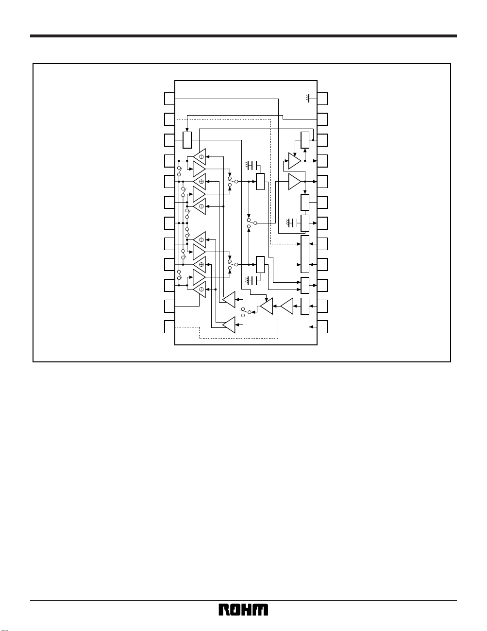
•
Block diagram
123456789101112
24 23 22 21 20 19 18 17 16 15 14 13
PRE
PRE
ENVE
PRE
PRE
ENVE
RF
DET PEAK ENVE LOGIC COMP MUTE
REC
AGC
SP EP
DET
GND 2
REC LEVEL ADJ
PB AGC OUT
PB RF OUT
AT ENVE PEAKING
AT ENVE OUT
H SYNC IN
DFF IN
ENVE COMP OUT
REC IN
AT ENVE FB
EP / SP CTRL
REC AGC FILTER
REC + OUT 1
GND 1
REC + OUT 2
REC DCFB 2
TP / PB / EE / REC CTRL
PB AGC FILTER
PRE IN 1
PRE IN 2
PRE IN 3
PRE IN 4
V
CC
AGC
(REC - OUT 1)
(REC - OUT 2)
(REC - OUT 3)
(REC - OUT 4)
(REC DCFB 1)
V
CC
Page 3
3
Video ICs BA7184S
•
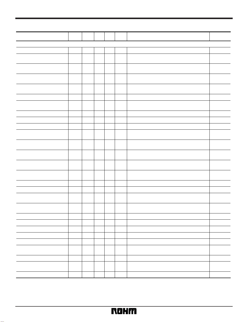
Electrical characteristics (unless otherwise noted, Ta = 25°C, VCC = 5.0V and f = 4.0MHz)
Parameter Symbol
Min.
Typ. Max. Unit
Measurement
circuit
— 27 45 mA Fig. 1
G
VP1
52 56 60 dB Fig. 1
G
VP2
52 56 60 dB Fig. 1
G
VP3
52 56 60 dB Fig. 1
G
VP4
52 56 60 dB Fig. 1
– 1.5 — + 1.5 dB Fig. 1
– 8 – 1.7 — dB Fig. 1
— – 42 – 35 dBc Fig. 1
— – 50 – 35 dBc Fig. 1
V
OMP
0.8 1.2 — V
P-P
Fig. 1
CT
P
— – 45 – 30 dBc Fig. 1
——200 mV
P-P
Fig. 1
V
NIN
— 0.25 1.0µVrms Fig. 1
V
AGC
265 315 365 mV
P-P
Fig. 1
— 0.3 2.0 dB Fig. 1
– 8 – 3 — dB Fig. 1
R
ON5, 9
— 510
Ω
Fig. 1
VENV1
— 0.7 1.0 V Fig. 1
VENV2
2.4 2.9 3.4 V Fig. 1
VENV3
4.0 4.5 — V Fig. 1
VTH16H
3.5 — V
CC
V Fig. 1
VTH16L
0 — 1.2 V Fig. 1
VTH2H
3.5 — V
CC
V Fig. 1
V
TH2L
0 — 1.2 V Fig. 1
VTH12T
4.1 — V
CC
V Fig. 1
VTH12H
3.0 — 3.7 V Fig. 1
VTH12M
1.1 — 2.6 V Fig. 1
VTH12L
0 — 0.7 V Fig. 1
2HD
P
3HD
P
Iq
(P)
∆G
VP
∆G
Vf
∆V
ODC
∆V
AGC
∆G
VAF
Supply current
Voltage gain ch-1
Voltage gain ch-2
Voltage gain ch-3
Voltage gain ch-4
Voltage gain differential
Frequency characteristic
2nd harmonic distortion
3rd harmonic distortion
Maximum output level
Crosstalk
Output DC offset
Input conversion noise
AGC output level
AGC control sensitivity
AGC frequency characteristic
PB switch ON resistance
ENVE residual voltage
ENVE output level
ENVE saturation voltage
PRE ch 2 and 4 holding voltage
PRE ch 1 and 3 holding voltage
EP mode holding voltage
SP mode holding voltage
TP mode holding voltage
PB mode holdihg voltage
EE mode holding voltage
REC mode holding voltage
∗
2 Guaranteed design values.
Note: dBc: dB below carrier (used to express relative level from carrier reference for convenience sake)
No signal
Pin 4 input = 0.3mV
P-P
, pin 2: L, pin 16: L,
pin 20 output measurement
Pin 6 input = 0.3mV
P-P
, pin 2: L, pin 16: H,
pin 20 output measurement
Pin 8 input = 0.3mV
P-P
, pin 2: H, pin 16: L,
pin 20 output measurement
Pin 10 input = 0.3mV
P-P
, pin 2: H, pin 16: H,
pin 20 output measurement
∆G
VP
= G
VP1
– G
VP2, GVP3
– G
VP4
Pin 20 output level difference for f = 8.0 / 1.0MHz,
V
IN
= 0.3mV
P-P
.
V
IN
= 0.3mV
P-P
, 8.0MHz spurious
V
IN
= 0.3mV
P-P
, 12.0MHz spurious
∗
2
When pin 20 output 2nd harmonic distortion is – 30dBc
Pin 20 output level difference for pin 2: H / L, pin 16: H / L.
Pin 20 output DC offset for pin 2: H / L, pin 16: H / L.
Rg = 10Ω, input conversion of pin 20 output noise
∗
2
VIN = 0.3mV
P-P
, pin 21 output measurement
Pin 21 output level differential for V
IN
= 0.15 to 0.6mV
P-P
.
f = 8.0 / 1.0MHz, V
IN
= 0.3mV
P-P
∗
2
Pin 5 and pin 9 impedance
∗
2
Pin 18 output measurement when no signal
Pin 18 output measurement when pin 20
output = 400mV
P-P
Pin 18 output measurement for large signal
Pin 16 DC voltage for ch 2 and 4 operation
Pin 16 DC voltage for ch 1 and 3 operation
Pin 2 DC voltage for EP mode
Pin 2 DC voltage for SP mode
Pin 12 DC voltage for TRICK PLAY mode
Pin 12 DC voltage for PB mode
Pin 12 DC voltage for REC MUTE mode
Pin 12 DC voltage for REC mode
Conditions
〈Playback system〉
(
Pin 12: H
)
Page 4

4
Video ICs BA7184S
Parameter Symbol Min. Typ. Max. Unit Conditions
— 67 100 mA Fig. 2
I
OAR1
27 30 33 mA
P-P
Fig. 2
I
OAR2
24 27 30 mA
P-P
Fig. 2
— 0.3 2.0 dB Fig. 2
– 8 – 3 — dB Fig. 2
2HD
R
— – 45 – 35 dBc Fig. 2
3HD
R
— – 50 – 35 dBc Fig. 2
CMD
R
— – 50 – 35 dBc Fig. 2
I
OMR
40 50 — mA
P-P
Fig. 2
– 2.0 – 0.3 — dB Fig. 2
MU
R
— – 45 – 35 dBc Fig. 2
V
TH17H
2.8 — VCCV Fig. 2
V
TH17L
0 — 1.2 V Fig. 2
Iq
(R)
∆I
OAR
∆I
OAF
∆I
ORL
Measurement
circuit
No signal
Pin 14 input = 125mV
P-P
, pin 2: L, pin 5
output measurement
Pin 14 input = 125mV
P-P
, pin 2: H, pin 9
output measurement
Pin 14 input = 62.5mV
P-P
, to 250mV
P-P
, pin 5
output level differential
f = 8.0 / 1.0MHz, pin 14 input = 125mV
P-P
,
∗
2
Pin 14 input = 125mV
P-P
, 8MHz spurious
Pin 14 input = 125mV
P-P
, 12.0MHz spurious
∗
2
4.0MHz ± 630kHz spurious
∗
2
When pin 5 output 2nd harmonic distortion is – 30dB
Pin 5 output level difference when load
L: 8.2 and 12µH
∗
2
Pin 5 output level difference for pin 12: M / L
Pin 17 DC voltage to maintain recording
AGC operation.
Pin 17 DC voltage to maintain recording AGC stopped.
Quiescent current
Recording AGC level 1
Recording AGC level 2
AGC control sensitivity
AGC frequency characteristic
2nd harmonic distortion
3rd harmonic distortion
Cross modulation distortion
Maximum output level
Recording current load characteristic
Mute attenuation ratio
AGC mode holding voltage
AGC mode holding voltage
∗
2 Guaranteed design values.
Note: dBc: dB below carrier (used to express relative level from carrier reference for convenience sake)
〈Recording system〉 (Pin 12: L)
Page 5

5
Video ICs BA7184S
123456789101112
24 23 22 21 20 19 18 17 16 15 14 13
PRE
PRE
ENVE
PRE
PRE
ENVE
RF
DET PEAK ENVE LOGIC COMP MUTE
REC
AGC
SP
EP
DET
0.1µ
33k
1k
0.1µ
1k
0.1
µ
PRE IN 3
PRE IN 2
1k
0.1
µ
PRE IN 1
1k
0.1µ
PRE IN 4
0.1µ
PB: OPEN
3.9k
68p
390k
0.01µ
REC IN
H SYNC IN
AT ENVE OUT
AT ENVE
PEAKING
PB RF OUT
PB AGC OUT
33k
EP / SP CTRL
VCC
DFF IN
ENVE COMP OUT
AGC
0.1µ
10k
10
10
10
10
REC START ‘‘L’’
REC MUTE ‘‘L’’
TRICK PLAY ‘‘H’’
VCC 5V
22µ
C [F]
L [H]
Units: R [Ω]
Fig. 1
+
•
Measurement circuits
(Playback system)
Page 6

6
Video ICs BA7184S
123456789101112
24 23 22 21 20 19 18 17 16 15 14 13
PRE
PRE
ENVE
PRE
PRE
ENVE
RF
DET PEAK ENVE LOGIC COMP MUTE
REC
AGC
SP
EP
DET
0.1µ
33k
0.1µ
0.1µ
PB: OPEN
3.9k
68p
390k
0.01µ
ENVE COMP OUT
REC IN
H SYNC IN
AT ENVE OUT
PB RF OUT
PB AGC OUT
33k
EP / SP CTRL
REC LEVEL ADJ
8.2µ
0.1µ
8.2µ
0.1µ
8.2µ
0.1µ
8.2µ
VCC
DFF IN
AGC
10k
0.1µ
REC OUT 1
REC OUT 2
REC START ‘‘L’’
REC MUTE ‘‘L’’
TRICK PLAY ‘‘H’’
10
10
VCC 5V
22µ
Fig. 2
C [F]
L [H]
Units: R [Ω]
+
(Recording system)
Page 7

7
Video ICs BA7184S
•
Control system logic table
(1) DFF IN (pin 16)
• Playback input selection (head switching)
Control pin
EP / SP
L
H
H
L
L
H
DFF IN
Function
Selected playback input
Control voltage
V
CTRL16 [V]
3.5 ~ V
CC
0.0 ~ 1.2
—
—
Ch3 (PRE IN3 8pin)
Ch4 (PRE IN4 10pin)
Ch1 (PRE IN1 4pin)
Ch2 (PRE IN2 6pin)
(2) EP / SP control (pin 2)
• Recording output selection
• Playback input selection (see (1))
EP / SP
H
L
Function
Selected recording output
Control pin
Control voltage
V
CTRL2 [V]
3.5 ~ V
CC
0.0 ~ 1.2
EP (REC OUT 8, 9, 10pin)
SP (REC OUT 4, 5, 6pin)
(3) TP / PB / EE / REC CTRL (pin 12)
• Special playback / playback / recording mute / recording mode switching
Mode
PB / EE / REC
OT ON ON ON OFF OFF
H PB ON ON OFF OFF OFF
M OFF OFF OFF ON ON
L REC OFF OFF OFF OFF ON
• Pin 12 is biased internally in the IC. When open, PB mode is selected.
TRICK PLAY
REC MUTE
Control pin
Function
Control voltage
V
CTRL12 [V]
4.1 ~ V
CC
3.0 ~ 3.7
1.1 ~ 2.6
0.0 ~ 0.7
PRE AMP AT ENVE ENV COMP REC MUTE REC AMP
(4) H SYNC IN (pin 17)
• Special playback envelope comparator (ENVE COMP) output latch control.
• AGC operation control for recording.
2.8 ~ VCC
HON
L OFF 0.0 ~ 1.2
ENVE COMP
Set at falling edge
—
H SYNC
Control voltage
V
CTRL17 [V]
Control pin Function
AGC detector
(5) ENVE COMP OUT (pin 15)
• Outputs playback envelope comparator data for special playback.
H
L
Ch1 or Ch2 > Ch3 or Ch4
ENVE COMP
Ch1 or Ch2 < Ch3 or Ch4
Function
Playback input level
Control pin
Page 8

8
Video ICs BA7184S
123456789101112
24 23 22 21 20 19 18 17 16 15 14 13
PRE
PRE
ENVE
PRE
PRE
ENVE
RF
DET PEAK ENVE LOGIC COMP MUTE
REC
AGC
SP
EP
DET
0.1
µ
33k
0.1
µ
0.1
µ
PB: OPEN
3.9k
22
µ
68p
390k
0.01
µ
ENVE COMP OUT
H SYNC IN
AT ENVE OUT
PB RF OUT
PB AGC OUT
33k
EP / SP CTRL
REC LEVEL ADJ
0.1
µ
0.1
µ
0.1
µ
REC Y IN
REC C IN
AB AB
EP HEAD
33k
PEAKING
AT ENVE
AT ENVE
GAIN
V
CC
DFF IN
AGC
10k
0.1
µ
SP HEAD
V
CC
5V
REC MUTE
‘‘L’’
REC START
‘‘L’’
TRICK PLAY
‘‘H’’
EP
‘‘H’’
Fig. 3
C [F]
L [H]
Units: R [Ω]
+
•
Application example
SDIP24
0.51Min.
6.5 ± 0.3
0.3 ± 0.1
7.62
3.4 ± 0.2
22.9 ± 0.3
0.5 ± 0.11.778
13
12
24
1
3.95 ± 0.3
0° ~ 15°
•
External dimensions (Units: mm)
 Loading...